

Page 1
SWITCH-MODE SOLENOID DRIVER
HIGH VOL TAGE OPERATION (UP TO 50V)
HIGH OUTPUT CURRENT CAP ABILITY (UP TO 4A)
LOW SA TURATION VOLTAGE
TTL-COM PATIBLE INPUT
OUTPUT SHORT CIRCUIT PROTECTI ON (TO
GROUND, TO SUPPLY AND ACROSS THE
LOAD)
THERMAL SHU TDOWN
OVERDRIVING PROTECTION
LATCHED DIAGNO S TIC OU TP UT
DESCRIPTION
The L294 is a monolithic switched mode solenoid
driver designed for fast, high current applications
such as hummer and needle driving in printers and
electronic typewriters. Power dissipation is reduced by efficient s wit c hm od e o pe ra ti on . A n e xtra
L294
Multiwatt 11
ORDER CODE : L294
feature of the L294 is a latched diagnostic output
which indicates when the output is short circuited.
The L294 is supplied in a 1 1-lead Multiw att® plastic power package.
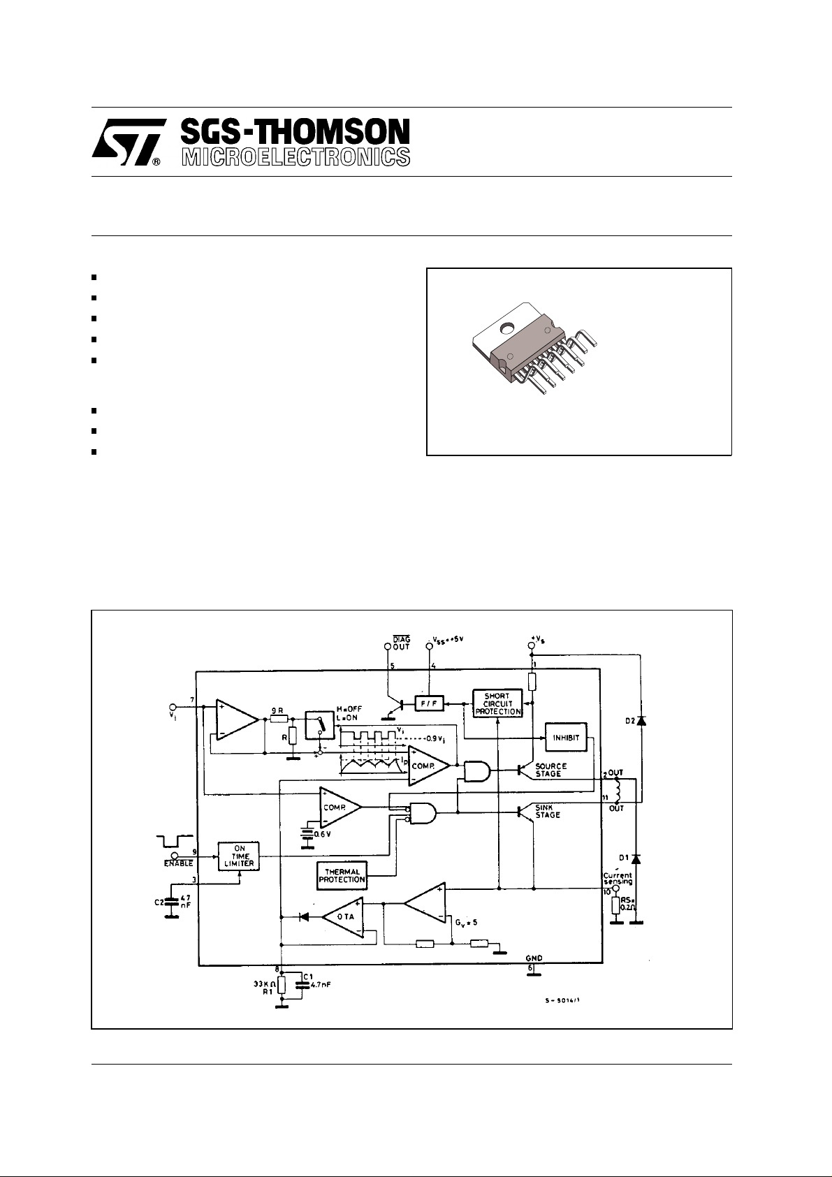
BLOCK DIAGR A M
October 1991
1/8
Page 2

L294
ABSOLUTE MAXIMUM RATING
Symbol Parameter Value Unit
V
s
V
SS
V
EN
I
p
P
tot
T
, T
stg
Power Supply Voltage 50 V
Logic Supply Voltage 7 V
Enable Voltage 7 V
Peak Output Current (repetitive) 4.5 A
Total Power Dissipation (at T
Storage and Junction Temperature - 40 to 150
j
CONNECT IO N DIAG RA M (top view)
= 75 °C)
case
25 W
°C
THERMAL DATA
Symbol Parameter Value Unit
Rth-j-case Thermal resistance junction-case Max 3
2/8
°C/W
Page 3

L294
ELECTRICAL CHARACTERISTICS (refer to the test circuit, Vs = 40 V, Vss = 5V, T
= 25 °C, unless
amb
otherwise specified)
Symbol Parameter Test conditions Min. Typ. Max. Unit
V
I
V
I
ss
V
I
V
ENABLE
I
ENABLE
I
load
V
sat H
V
sat L
V
sat H + VsatL
I
leakage
K On Time Limiter Constant (°) V
V
DIAG
I
DIAG
V
pin
V
pin
V
SENS
(°) After a time interval t
(°°) See the block diagram.
(°°°) Allowed range of V
Power Supply Voltage (pin 1) Operative Condition 12 46 V
s
Quiescent Drain Current (pin 1) V
d
Logic Suply Voltage (pin 4) 4.5 7 V
ss
Quiescent Logic Supply
Current
Input Voltage (pin 7) Operating Output 0.6 V
i
= H 20 30
ENABLE
Vi ≥ 0.6V; V
V
= L 5 8 mA
DIAG
ENABLE
= L
70
DIAG Output at High Impedance 10 100
Non-operative Output 0.45
Input Current (pin 7)
i
≥ 0.6V
V
i
V
≤ 0.45V
i
-3
-1
Enable Input Voltage (pin 9) Low Level -0.3 0.8
High Level 2.4
Enable Input Current (pin 9) V
/ ViTrasconductance
Source Output Saturation
= L -100
ENABLE
= H 100
V
ENABLE
V
= 0.2 Ω
R
S
= 1V 0.95 1 1.05
i
V
= 4V 0.97 1 1.3
i
Ip = 4A 1.7 V
Voltage
Sink Output Saturation Voltage Ip = 4A 2 V
Total Saturation Voltage Ip = 4A 4.5 V
Output Leakage Current
Diagnostic Output Voltage
Rs = 0.2Ω; Vi ≤ 0.45 V
= L 120
ENABLE
I
= 10 mA 0.4 V
DIAG
(pin 5)
Diagnostic Leakage Current
V
= 40V 10
DIAG
(pin 5)
8
OP AMP and OTA CD V oltage
Gain (°°)
10
V
= 100 to 800 mV 5
pin 10
Sensing Voltage (pin 10) (°°°) 0.9 V
= KC2, the output stages are disabled.
max
without intervention of the short circuit p rotect ion.
SENS
1mA
mA
µA
µA
V
µA
A/V
µA
3/8
Page 4

L294
CIRCUIT OPERATION
The L294 work as a trasconductance amplifier: it
can supply an output current directly proportional
to an input voltage level (V
complete switching control of the output current
waveform (see fig. 1).
The following explanation refers to the Block Diagram, to fig. 1 and to the typical application circuit
of fig. 2.
time is fixed by the width of the Enable input
The t
on
signal (TTL com patible): it is active low and enables
the output stages "source" and "sink". At the end of
, the load current I
t
on
and D2, allowing fast current turn-off.
The rise time t
teristics, o n V
pin 1). During the t
, depends on the load charac-
r
and on the supply voltage value (Vs,
i
on
voltage signal by means of the external sensing
resistance R
connected to pin 10. This signal,
s
amplified by the op amp and converted by the
transconductance amplifier OTA, charges the external RC network at pin 8 (R1, C1) . The voltage at
this pin is sensed by the inverting input of a comparator. The voltage on the non-inverting input of
this one is fixed by the external voltage V
After t
, the comparator switches and the output
r
stage "source" is switched off. The comaprator
output is confirmed by the voltage on the non-inverting input, which decreases of a costant fraction
(1/10), allowing hysteresis operation. The
of V
i
current in the load now flow through D1.
Two Cases are possible: the time constant of the
recirculation phase is higher than R1.C1; the time
constant is lower than R1.C1. In the first case, the
voltage sensed in the non-inverting input of the
comparator is just the value proport ional to I
the second case, when the current decreases too
quickly, the comparator senses the voltage signal
stored in the R1 C1 network.
In the first case t
depends on the load charac-
1
teristics, while in the second case it depends only
on the value of R1. C1.
In the other words, R1. C1 fix es the minimum value
)t1 ≥ 1/10 R1.C1. Note that C1 should be
of t
1
chosen in the range 2.7 to 10 nF for stability reasons of the OTA).
, the comparator switches again: the output
After t
1
is confirmed by the voltage on the non-inverting
input, which reaches V
Now the cycle s tarts again: t
same characteris tics as t
). Fyrthermore, it allows
i
recirculates through D1
load
time, I
again (hysteresis).
i
r
is converter into a
load
, t4 and t6 have the
2
, while t3 and t5 are similar
(pin 7).
i
load
. In
to t
. The peak current Ip depends on Vi as shown
1
in the typical transfer function of fig.3.
It can be seen that for V
lower than 450 mV th e
i
device is not operating.
greater than 600 mV, the L294 has a tran-
For V
i
sconductance of 1A/V with R
= 0.2Ω. For Vi in-
s
cluded between 450 and 600 mV, the operation is
not guaranteed.
The order parts of the device have protection and
diagnostic functions. At pin 3 is connected an external capacitor C2, charged at costant current
when the Enable is low.
After a time interval equ al to K C2 (K is defined in
the table of Electrical Characteristics and has the
dimensions of ohms) the output stages are
switched off independently by the Input signal.
This avoids the load being driven in conduction for
an excessive period of time (overdriving protection). The action of this protection is shown in fig.
1b. Note that the voltage ramp at pin 3 starts
whenever the Enable signal becomes active (low
state), regardless of the Input signal. To reset pin 3
and to restore the normal conditions, pin 9 must
return high.
This protection can be disabled by grounding pin 3.
The thermal protection included in the L294 has a
hysteresis.
It switches off the output stages whenever the
junction temperature increases too much. After a
fall of about 20°C, the circuit starts again.
Finally, the device is protected against any type of
short circuit at the outputs : to ground, t o supply and
across the load.
When the source stage current is higher than 5A
and/or when the pin 10 voltage is higher then 1V
(i.e. for a sink current greater than 1V/R
) the output
s
stages are switched off and the device is inhibited.
This condition is indicated at the open-collector
output DIAG (pin 5); the internal flip-flop F/F
changes and forces the output transis tor int o s aturation. The F/F must be supplied independently
through V
(pin 4). The DIAG signal is reset and
ss
the output stages ar e still operativ e by switching the
device on again. After that, two cases are possible:
the reason for the "bad operation" is still present
and the protection acts again; the reason has been
removed and the device starts to work properly .
4/8
Page 5

Figure 1. Outp ut Current Waveforms.
Figure 2. Test and T ypi cal Ap pli cati on Circui t.
L294
D1 : 3A fast diode
200 ns
Figure 3. Peak Output Curren t vs. Input
Voltage.
trr ≤
}
Figure 4. Output Satu rati on Voltage vs.
Peak Output Current.
5/8
Page 6

L294
Figure 5. Safe Oper atin g Areas.
Figure 6. Turn-off Phase.
CALCULATION OF THE SWITCHIN G TIMES
Referring to the block diagram and to the waveforms of fig. 1, it is possible to calculate the switching tim es
by means of the following relationships.
t
= −
r
tf = −
L
In (1 −
R
L
L
In
R
L
V2 +
R
V
V2
R
L
• Ip )
1
• I
L
o
where : V1 = V
- V
s
sat L
- V
where : V2 = Vs + VD1 + V
IK ≤ Io ≤ I
p
sat H
D2
_ V
R sens
Io is the value of the load current at the end of ton.
t
= t3 = t5 = ...
1
t
= t4 = t6 = ...
2
Note that the time interval t
In
L
p
R
0.9 I
L
)
L
I
p
RL + V3
p
1
10
R1 C1
L
−
=
= −
= t3 = t5 = ... takes the longer value between case a) and cas e b). The swit ching
1
a)
R
b) − R1 C1 In 0.9 ≅
− I
In (
V1
V1 − IK R
L
R
L
• RL + V3
where
V3 = V
sat L
+ V
R sens
+ V
D1
frequency is alway s :
f
switching
=
t
1
1
+ t
2
In the case a) the main regulation loop is always closed and it forces :
I
= (0.9 ± S) Ip where : S = 3 % @ Vi = 1 V
K
S = 1.5 % @ Vi = 4 V
In the case b), the same loop is open in the recirc ulation phase and I
, which is always lower than 0.9 Ip,
K
is obtained by means of the following relationship.
= Ip e −
I
K
t
1
R
L
L
−
V3
(1 − e −
R
L
t
R
1
L
)
L
With the typical application circuit, in the conditions Vs = 40V , Ip = 4A, the following switching times result:
= 255 µs tf = 174 µs @ Io = I
t
r
p
a) 70 µs
t1 =
b) 16 µs t2 = 29 µs f = 10.2 KHz
6/8
Page 7

MULTIWATT11 PACKAGE MECHANICAL DATA
DIM.
MIN. TYP. MAX. MIN. TYP. MAX.
A 5 0.197
B 2.65 0.104
C 1.6 0.063
D 1 0.039
E 0.49 0.55 0.019 0.022
F 0.88 0.95 0.035 0.037
G 1.57 1.7 1.83 0.062 0.067 0.072
G1 16.87 17 17.13 0.664 0.669 0.674
H1 19.6 0.772
H2 20.2 0.795
L 21.5 22.3 0.846 0.878
L1 21.4 22.2 0.843 0.874
L2 17.4 18.1 0.685 0.713
L3 17.25 17.5 17.75 0.679 0.689 0.699
L4 10.3 10.7 10.9 0.406 0.421 0.429
L7 2.65 2.9 0.104 0.114
M 4.1 4.3 4.5 0.161 0.169 0.177
M1 4.88 5.08 5.3 0.192 0.200 0.209
S 1.9 2.6 0.075 0.102
S1 1.9 2.6 0.075 0.102
Dia1 3.65 3.85 0.144 0.152
mm inch
L294
7/8
Page 8

L294
Information furnished is believed to be accurate and reliable. However, SGS-THOMSON Microelectronics assumes no responsibility for the
consequences of use of such information nor for any infringement of patents or other rights of third parties which may result from its use. No
license is granted by implication or otherwise under any patent or patent rights of SGS -TH OMS O N Microelectronics. Specifications m entioned
in this publication are subject to change without notice. This publication supersedes and replaces all information previously supplied.
SGS-THOMSON Microelectronics pr oducts are not authorized for use as critical components in life support devices or system s without express
written approval of SGS-THOMSON Microelectronics.
© 1994 SGS-THOMSON Microelectronics - All Rights Reserved
SGS-THOMSON Microelectronics GROUP OF COMPANIES
Australia - Brazil - France - Germany - Hong Kong - Italy - Japan - Korea - Malaysia - Malta - Morocco - The Netherlands - Singapore -
Spain - Sweden - Switzerland - Taiwan - Thaliand - United Kingdom - U.S.A.
8/8
 Loading...