

Page 1

LOW DROP DUAL POWER OPERATIONAL AMPLIFIER
■ OUTPUT CURRENT TO 1 A
■ OPERATES AT LOW VOLTAGE S
■ SINGLE OR SPLIT SU PPL Y
■ LARGE COMMON-MODE AND
DIFFERENTIAL MODE RANGE
■ LOW INPUT OFFSET VOLTAGE
■ GROUND COMPATIBLE INPUTS
■ LOW SATURATION VOLT AGE
■ THERMAL SHUTDOWN
■ CLAMP DIODE
L2720D
DESCRIPTION
The L2720D is a monolithic integrated circuits in SO16 package, intended for use as power operational
amplifiers in a wide range of appli cations including
servo amplifiers and power supplies.
It is particularly indicated for driving, inductive loads,
as motor and finds applications in compact-disc VCR
automotive, etc.
The high gain and high output power capability provide superior performance whatever an operational
amplifier/power booster combination is required.
BLOCK DIAGRAM
SO-16 (narrow)
ORDERING NUMBER: L2720D
September 2002
1/6
Page 2

L2720D
PIN CONNECTION
(Top view)
SCHEMATIC DIAGRAM
(one section)
ABSOLUTE MAXIMUM RATINGS
Symbol Parameter Value Unit
2/6
V
V
V
V
I
o
I
p
P
tot
T
op
T
stg
Supply Voltage 28 V
S
Peak Supply Voltage (50ms) 50 V
S
Input Voltage Vs
i
Differential Input Voltage ±Vs
i
DC Output Current 1 A
Peak Output Current (non repetitive) 1.5 A
Power Dissipation at T
= 50°C 800 mW
amb
Operating Temperature – 40 to 85 °C
, TjStorage and Junction Temperature – 40 to 150 °C
Page 3
L2720D
THERMAL DATA
Symbol Parameter Value Unit
R
th j-amb
Thermal Resistance Junction to ambient Typ. 95 °C/W
ELECTRICAL CHARACTERISTICS
(Vs = 2 4V, T
= 25°C unless otherwise specified)
amb
Symbol Parameter Test Conditions Min. Typ. Max. Unit
V
Single Supply Voltage 4 28 V
s
V
Split Supply Voltage ± 2 ± 14 V
s
Quiescent Drain Current
I
s
Input Bias Current 0.2 1 µA
I
b
V
Input Offset Voltage 10 mV
os
Input Offset Current 100 nA
I
os
V
V
o
--- -=
2
V
= 24V
s
Vs = 8V
10
15
9
15
mA
mA
SR Slew Rate 2V/µs
B Gain-bandwidth Product 1.2 MHz
R
Input Resistance 500 kΩ
i
O.L. Voltage Gain f = 100Hz
G
v
f = 1kHz
e
Input Noise Voltage B = 22Hz to 22kHz 10 µV
N
Input Noise Voltage 200 pA
I
N
70 80
60
dB
CMR Common Mode Rejection f = 1kHz 66 84 dB
SVR Supply Voltage Rejection f = 100Hz; V
RG = 10kΩ; Vs = ±12V
V
= 0.5V; Vs = ±6V
R
V
DROP(H)
V
DROP(L)
Drop voltage high Vs = ±2.5V to ±12V Ip = 100mA
Drop voltage low Vs = ±2.5V to ±12V Ip = 100mA
Channel Separation f = 1KHz; Vs = 24V
C
s
RL = 10Ω; Vs = 6V
G
= 30dB
v
T
Thermal Shutdown Junction
sd
= 24V
s
60
Ip = 500mA
Ip = 500mA
70
dB
75
80
0.7
11.5
0.3
0.5 1
60
dB
60
145 °C
V
V
Temperature
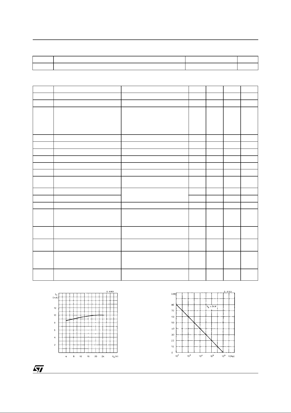
Figure 1. Quiescent Current vs. S upply Voltage Figure 2. Open Loop Gain vs. Frequency
3/6
Page 4
L2720D
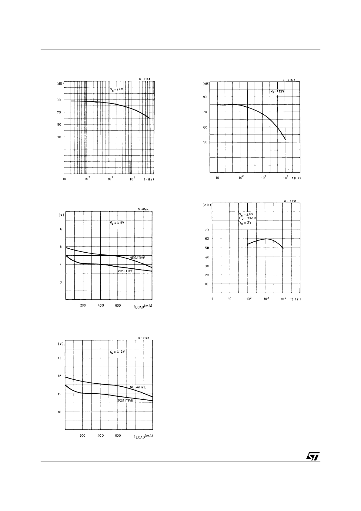
Figure 3. Comm on Mode Reje ct i on vs.
Frequency
Figure 4. Out put S wi ng v s. Load Current
(V
= ± 5V).
S
Figure 6. Supply Voltage rejection vs.
Frequency
Figure 7. Channel Separation vs. Frequency
Figure 5. Out put S wi ng v s. Load Current
(V
= ± 12V).
S
4/6
Page 5
L2720D
DIM.
MIN. TYP. MAX. MIN. TYP. MAX.
A 1.75 0.069
a1 0.1 0.25 0.004 0.009
a2 1.6 0.063
b 0.35 0.46 0 .014 0.018
b1 0.19 0.25 0.007 0.010
C 0.5 0.020
c1 45˚ (typ.)
D (1) 9.8 10 0.386 0.394
E 5.8 6.2 0.228 0.244
e 1.27 0.050
e3 8.89 0.350
F (1) 3.8 4 0.150 0.157
G 4.6 5.3 0.181 0.209
L 0.4 1.27 0.016 0.050
M 0 .62 0.024
S
mm inch
8˚(max.)
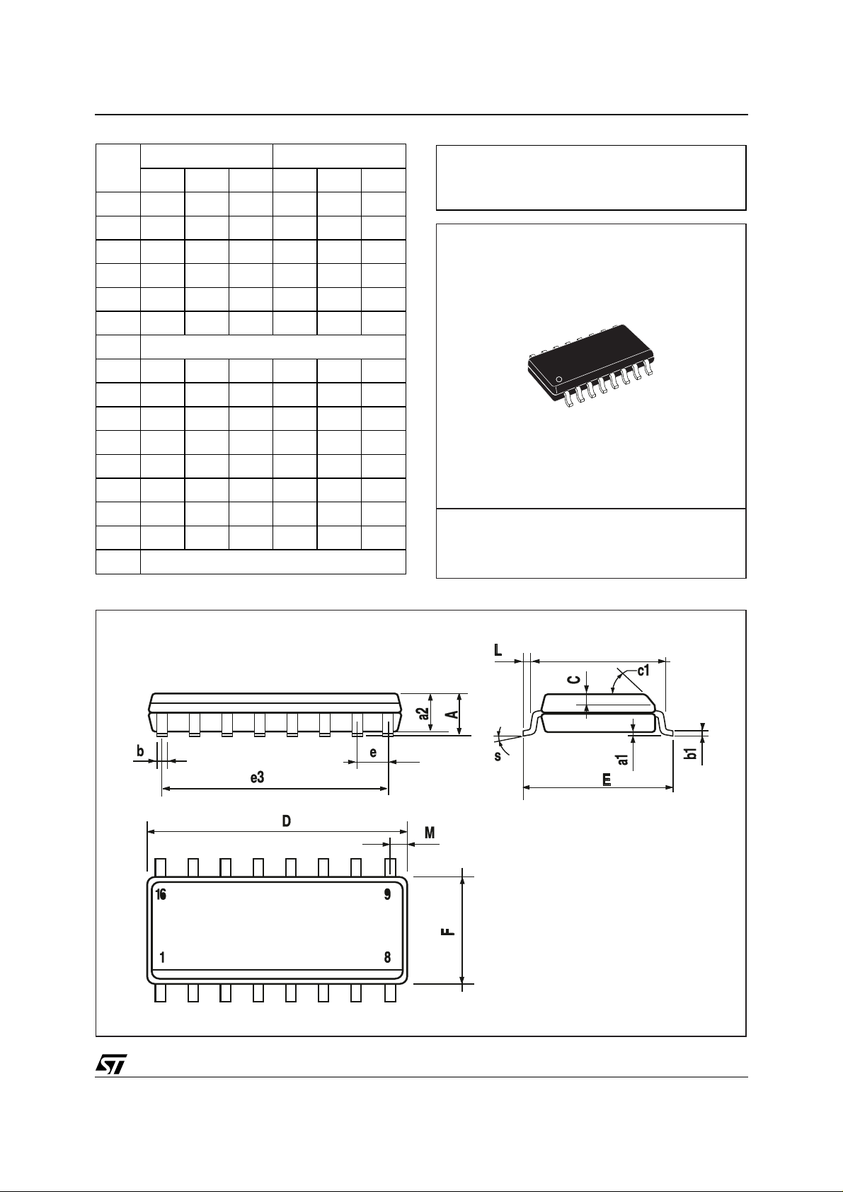
OUTLINE AND
MECHANICAL DATA
SO16 Narrow
(1) D and F do not include mold flash or protrusions. Mold flash or potrusions shall not exceed 0.15mm (.006inch).
5/6
Page 6

L2720D
Information furnished is believed to be accurate and reliable. However, STMicroelectronics assumes no responsibility for the consequences
of use of such information nor for any infringement of patents or other rights of third parties which may result from its use. No license is granted
by implic ation or otherwise under any patent or patent r i ght s of STMi croelectr oni cs. Spec i fications mentioned i n this publication are subject
to change without notice. This publication supersedes and replaces all information previously supplied. STMicroelectronics product s are not
authorized for use as cri tical comp onents in lif e support devi ces or systems without express written approva l of STMicroel ectronics.
The ST logo is a registered trademark of STMicroelectronics
2002 STMicroelectronics - All Ri ghts Rese rved
Austra lia - Brazil - Canada - Chi na - F i nl and - Franc e - Germany - Hong Kong - In di a - Israel - Ita l y - J apan -Malaysia - Malta - Morocco -
Singap ore - Spain - Sw eden - Switze rl and - Unit ed K i ngdom - United States .
STMicroelectronics GROUP OF COMPANIES
http://www.s t. com
6/6
 Loading...