

Page 1
L165
3APOWER OPERATIONALAMPLIFIER
OUTPUTCURRENT UP TO3A
LARGECOMMON-MODEANDDIFFERENTIAL
MODERANGES
SOAPROTECTION
THERMALPROTECTION
± 18V SUPPLY
Pentawatt
DESCRIPTION
The L165 is a monolithic integrated circuit in
Pentawatt package, intended for use as power
operational amplifier in a wide range of applications, including servo amplifiers and power supplies. The high gain and high output power
capabilityprovidesuperioreperformancewherever
an operational amplifier/power booster combina-
ORDERING NUMBER : L165V
tion is required.
ABSOLUTE MAXIMUM RATINGS
Symbol Parameter Value Unit
Supply voltage ± 18 V
V
s
V
V
T
Upper power transistor V
5V4
Lower power transistor V
4V3
Input voltage V
V
i
V
Differentialinput voltage
j
Peak output current (internally limited) 3.5 A
I
o
Power dissipation at T
P
tot
Storage and junction temperature -40 to 150
stg,Tj
CE
CE
=90°C20W
case
36 V
36 V
s
± 15
°C
V
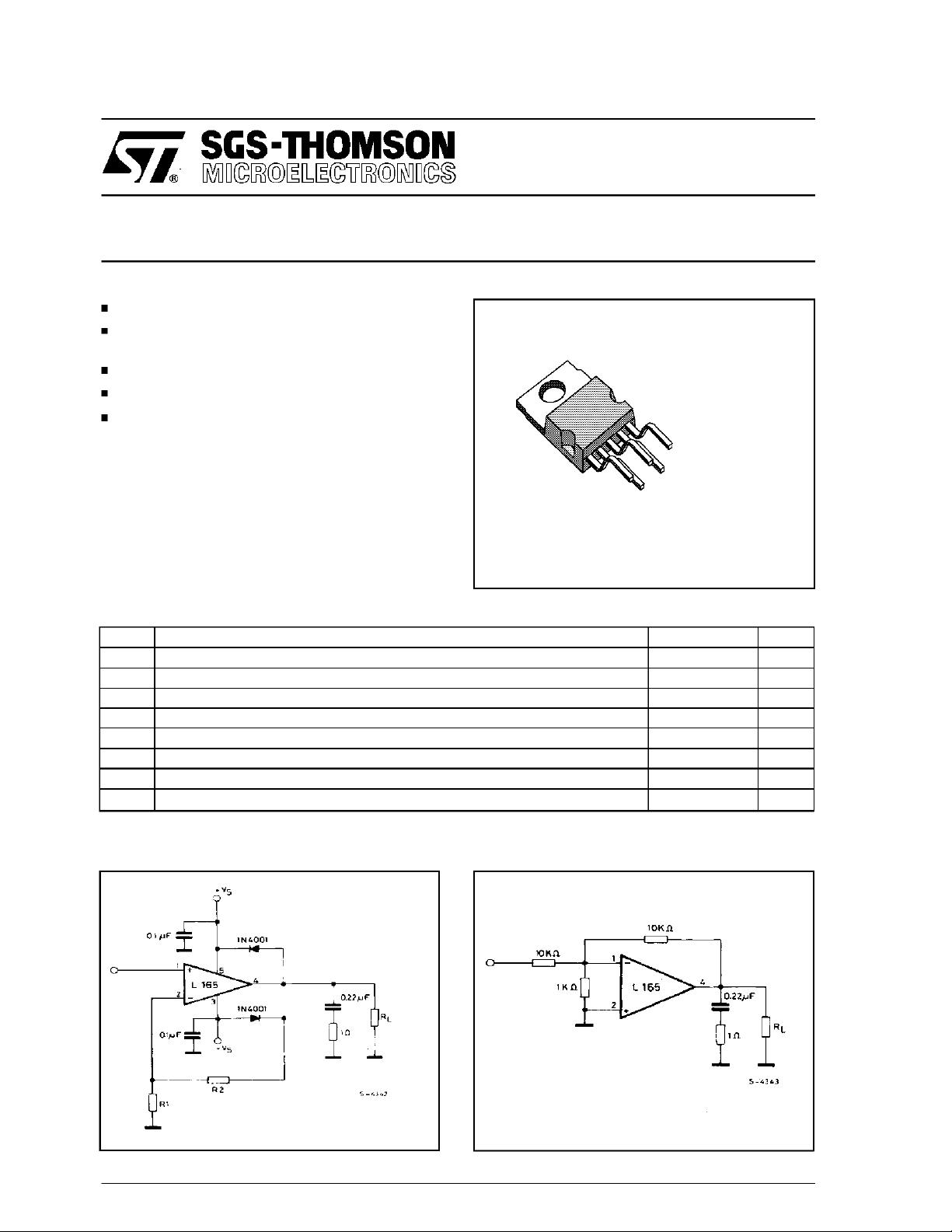
APPLICATION CIRCUITS
October 1991
Figure 2. Unity gain configuration.Figure 1. Gain > 10.
1/9
Page 2
L165
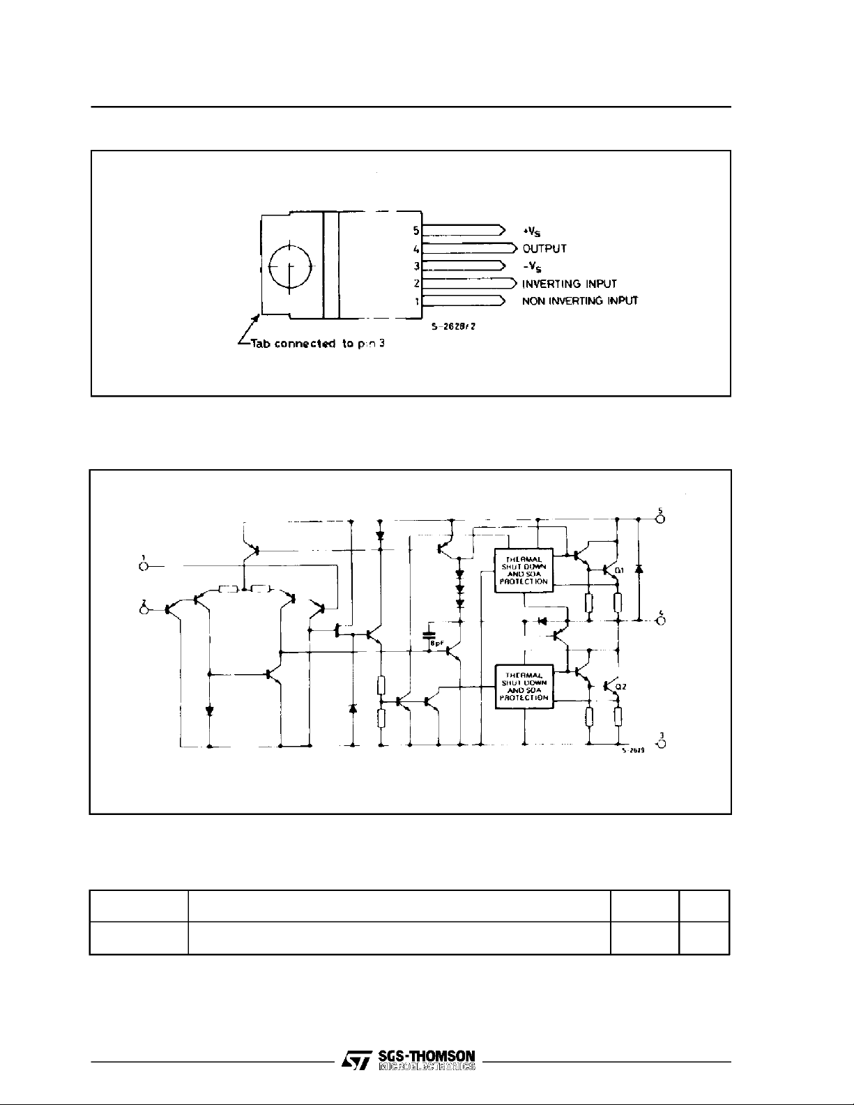
PIN CONNECTION (top view)
SCHEMATIC DIAGRAM
THERMALDATA
Symbol Parameter Value Unit
2/9
R
th-j-case
Thermal resistance junction-case max 3 °C/W
Page 3
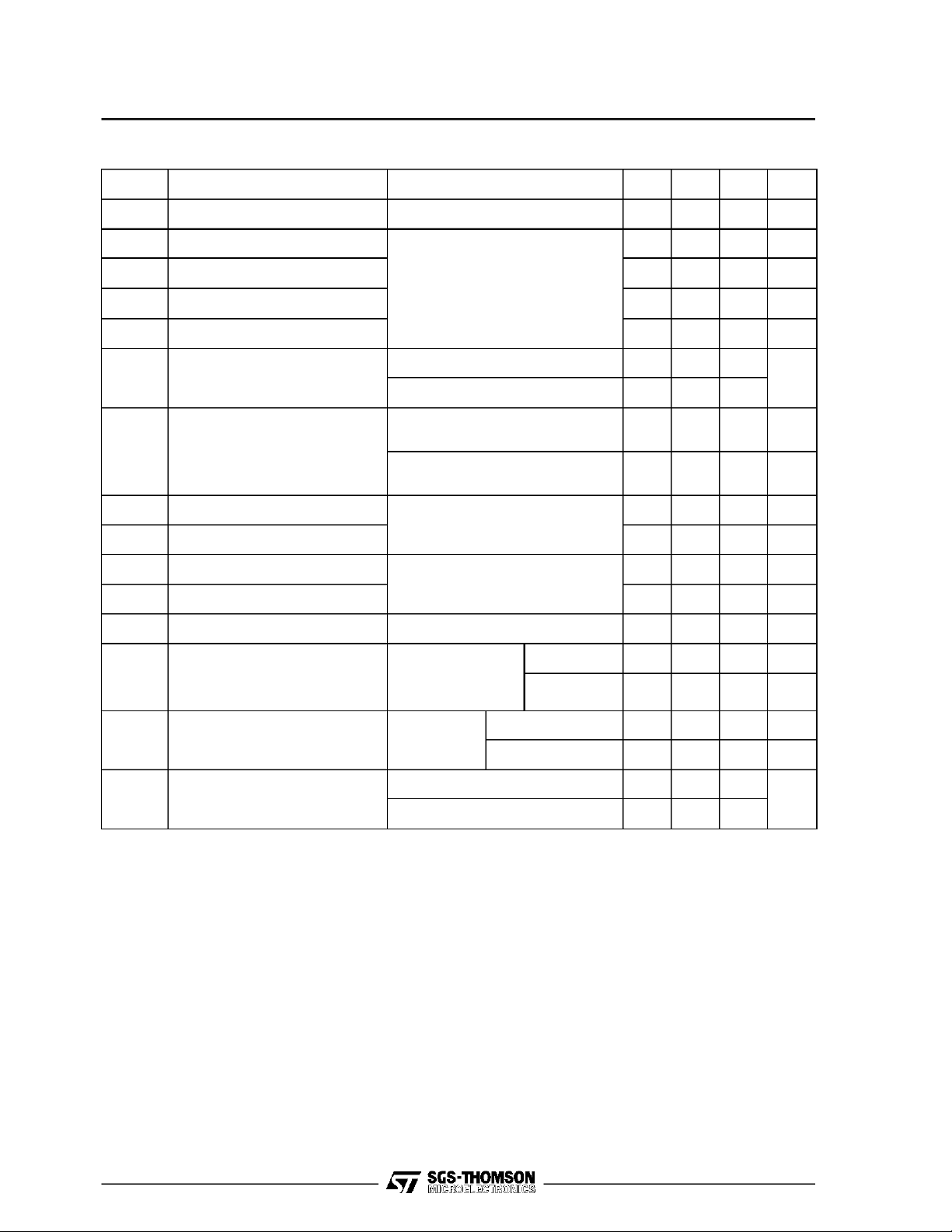
ELECTRICAL CHARACTERISTICS (VS= ± 15 V,Tj=25°C unless otherwise specified)
Symbol Parameter Test Conditions Min. Typ. Max. Unit
L165
V
V
I
Supply Voltage
s
Quiescent Drain Current
I
d
Input Bias Current 0.2 1
I
b
Input Offset Voltage ±
os
Input Offset Current ± 20 ± 200 nA
os
SR Slew-rate G
V
Output VoltageSwing f = 1 kHz Ip=0.3 A
o
R Input Resistance (pin 1)
G
e
VoltageGain (open loop) 80 dB
v
Input Noise Voltage
N
Input Noise Current 100 pA
i
N
CMR Common-mode Rejection
SVR Supply Voltage Rejection
± 6 ± 18
V
40 60 mA
= ± 18 V
V
s
2 ± 10
=10 8
v
G
=1(°)6
v
27
=3 A
I
p
f = 10 kHz Ip=0.3 A
I
=3 A
p
f = 1 KHz
B = 10 to 10 000 Hz
G
≤ 10 KΩ
R
g
R
=22KΩ
g
V
ripple
f
ripple
= 0.5 V
= 100 Hz
rms
=30dB 70 dB
v
G
v
dB G
100 500
=10 60 dB dB
= 100 40 dB
v
24
27
23
2 µ
µA
mV
V/µs
V
pp
V
PP
KΩ
V
I
Efficiency
T
Thermal Shut-down Case
sd
Temperature
f = 1 kHz
R
=4Ω
L
P
= 12 W 110
tot
P
= 6 W 130
tot
= 1.6 A; Po=5W 70 %
p
= 3 A; Po= 18 W 60 %
I
p
°C
3/9
Page 4
L165
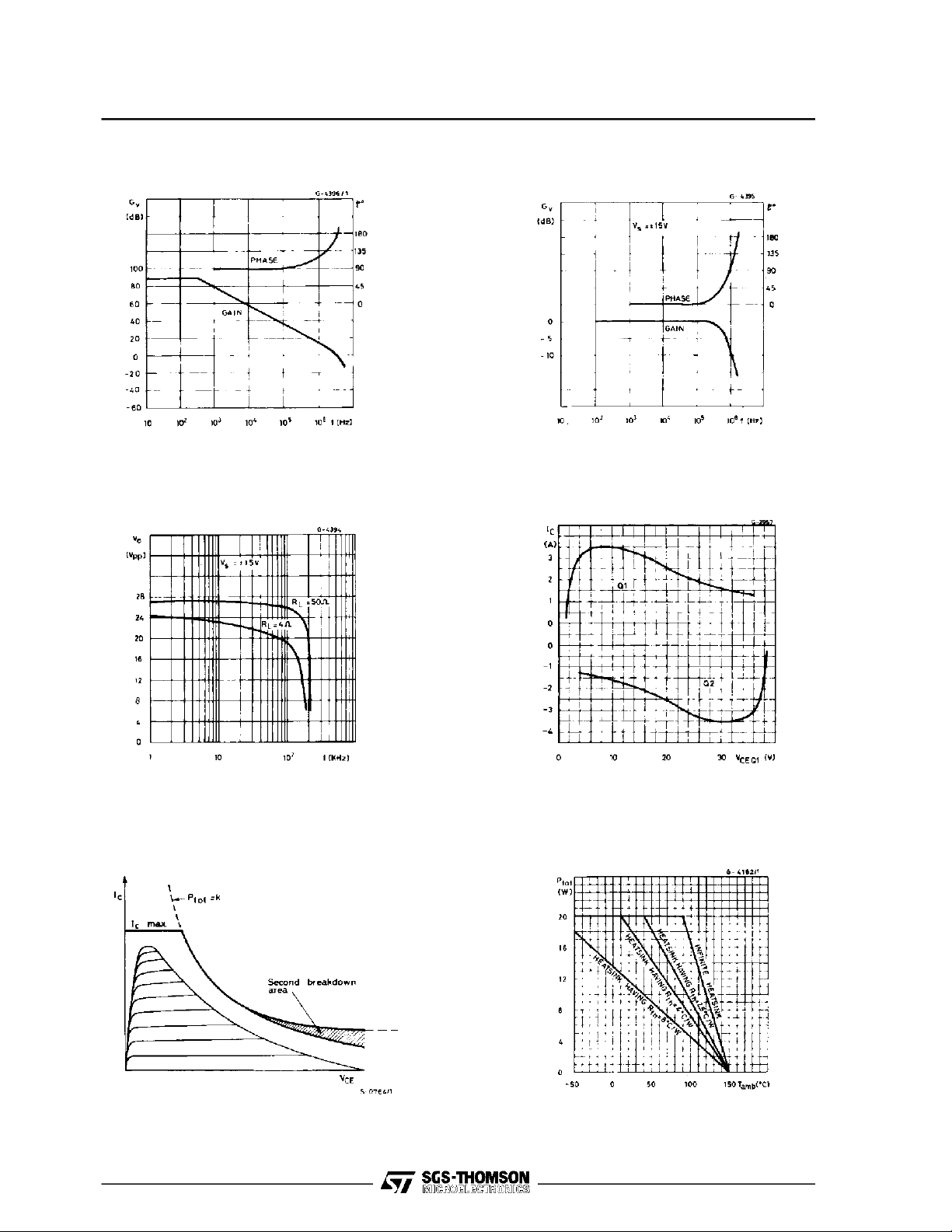
Figure 3. Open loop frequency response.
Fig ure 5. Lar ge s ig nal fre quenc y
response.
Figure4. Closedloopfrequencyresponse
(circuitof figure 2).
Figure 6. Maximum output current vs.
voltage [VCE ] a cross each output
transistor.
Figure7. Safeoperatingareaandcollector
characteristics of the protected power
transistor.
4/9
Figure 8 . Ma xi m um a l lowa ble pow er
dissipationvs. ambienttemperature.
Page 5
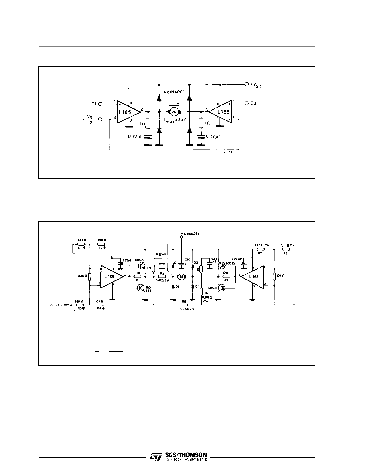
Figure 9. Bidirectional DC motor control with TTL/CMOS/µP compatible inputs.
Must beVS2≥ VS1E1, E2 = logic inputs
V
= logic supply voltage
S1
L165
Figure 10. Motor current control circuit with external power transistors(I
D1 to D4 : VF≤ 1.2 @ I = 4A
t
≤ 500 ns
rr
Note :The inputvoltage level is compatible with L291 (5-BIT D/Aconverter).
I
R4
M
The transfer function is :
=
V
Rx R3
i
motor
> 3.5A).
5/9
Page 6
L165
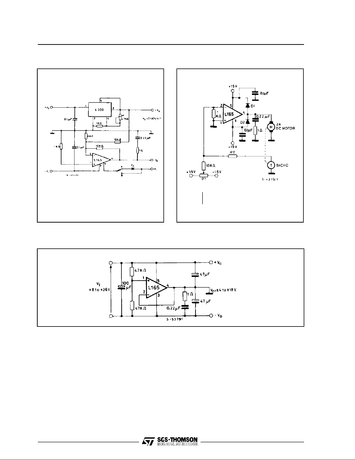
Figure11. High current tracking regulator.
A: for ± 18 ≤ Vi ± 32
Note: V
mustbe chosenin order toverify
z
2V
≤ 36V
i-Vz
B : for V
≤ ± 18V
i
Figure 12. Bidirectional speed control of DC
motor (Compensation networks not shown).
D1, D2 : VF ≤ 1.2V @ I =2A
t
≤ 500 ns
rr
Figure 13. Split power supply.
6/9
Page 7
L165
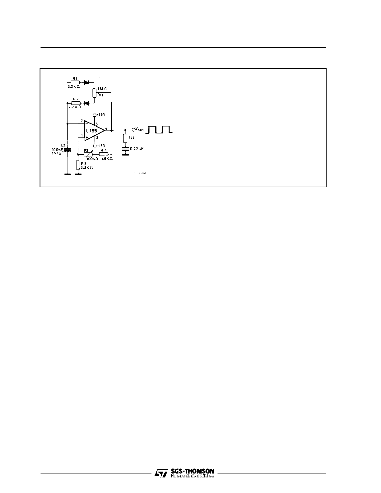
Figure14. Powersquarewaveoscillatorwithindependentadjustmentsforfrequencyand duty-cycle.
P1 : duty-cycle adjust
P2 : frequency adjust (f = 700 Hz with C1 =10 nF,P2 = 100
KΩ, f = 25Hz with C1 = 10 nF,P2 = 0)
7/9
Page 8
L165
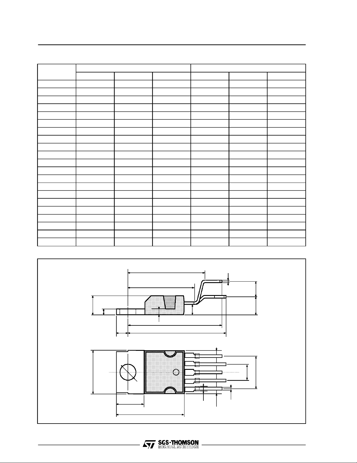
PENTAWATT PACKAGE MECHANICAL DATA
DIM.
MIN. TYP. MAX. MIN. TYP. MAX.
A 4.8 0.189
C 1.37 0.054
D 2.4 2.8 0.094 0.110
D1 1.2 1.35 0.047 0.053
E 0.35 0.55 0.014 0.022
F 0.8 1.05 0.031 0.041
F1 1 1.4 0.039 0.055
G 3.4 0.126 0.134 0.142
G1 6.8 0.260 0.268 0.276
H2 10.4 0.409
H3 10.05 10.4 0.396 0.409
L 17.85 0.703
L1 15.75 0.620
L2 21.4 0.843
L3 22.5 0.886
L5 2.6 3 0.102 0.118
L6 15.1 15.8 0.594 0.622
L7 6 6.6 0.236 0.260
M 4.5 0.177
M1 4 0.157
Dia 3.65 3.85 0.144 0.152
mm inch
A
H3
L
L1
C
D1
L5
Dia.
L7
L6
D
L2
L3
F1
H2
E
MM1
G1
G
F
8/9
Page 9

L165
Information furnished is believed to be accurate and reliable. However, SGS-THOMSON Microelectronics assumes no responsibility for the
consequences of use of such information nor for any infringement of patents or other rights of third parties which may result from its use. No
licenseis granted by implication or otherwise under any patent or patent rights of SGS-THOMSON Microelectronics. Specifications mentioned
in this publication are subject to change without notice. This publication supersedes and replaces all information previously supplied.
SGS-THOMSON Microelectronics products arenot authorized for use as critical componentsin life support devices or systems without express
written approval of SGS-THOMSON Microelectronics.
1994SGS-THOMSON Microelectronics - All Rights Reserved
SGS-THOMSON Microelectronics GROUP OF COMPANIES
Australia - Brazil -France -Germany - Hong Kong - Italy- Japan- Korea - Malaysia - Malta - Morocco - The Netherlands - Singapore -
Spain - Sweden - Switzerland - Taiwan - Thaliand - United Kingdom - U.S.A.
9/9
 Loading...