

Page 1
NIKO-SEM
Dual Input Ultra Low Dropout
Voltage Regulator (ULDO)
GENERAL DESCRIPTION
FEATURES
L1581 Series
TO-252
The L1581 is a positive and very low
dropout voltage regulator with 5A output
current capability. When supplying 2.5V or
2.8V on Motherboards or VGA Card where
both 5V and 3.3V supplies are available,
the superior dropout characteristics of the
L1581 result in reduced heat dissipation
compared to regular LDOs, thus allowing
heat sink reduction. The adjustable version
requires only two external resistors to set
the output. The L1581 features a low
dropout of less than 600mV and offers fast
transient response, remote sense, internal
limiting, thermal shutdown and safe
operating area protection of the output
device.
The L1581 is a five terminal adjustable
voltage regulator available in the popular 5
pin TO-252 packages.
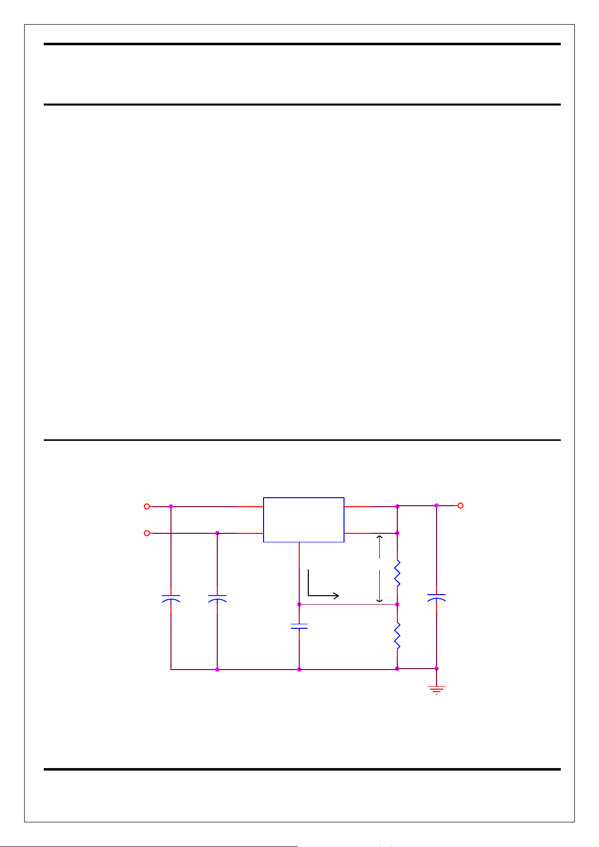
TYPICAL APPLICATION
Adjustable Output Parts
Vin
(2)
L1581X
z Low dropout voltage 600mV at rated load
current
z Remote sense operation
z Fast transient response
z 0.5% voltage reference initial accuracy
z Standard 5 terminal, Low cost TO-252
packages
APPLICATIONS
z 3.3V to 2.8V or 2.5V for Motherboards or
VGA Card
z Spilt plane microprocessor supplies
z Post regulator for switching supplies
35
OUTVin
Vout
Vctrl
C1
330uF
4
CTR'L
C2
10uF
0.033uF
C3
2
SENSE
ADJ
Iadj
Vo = Vref (1+R2/R1) + Iadj x R2
1
Vref
R1
C4
330uF
R2
1
OCT-11-Y02
Page 2
NIKO-SEM
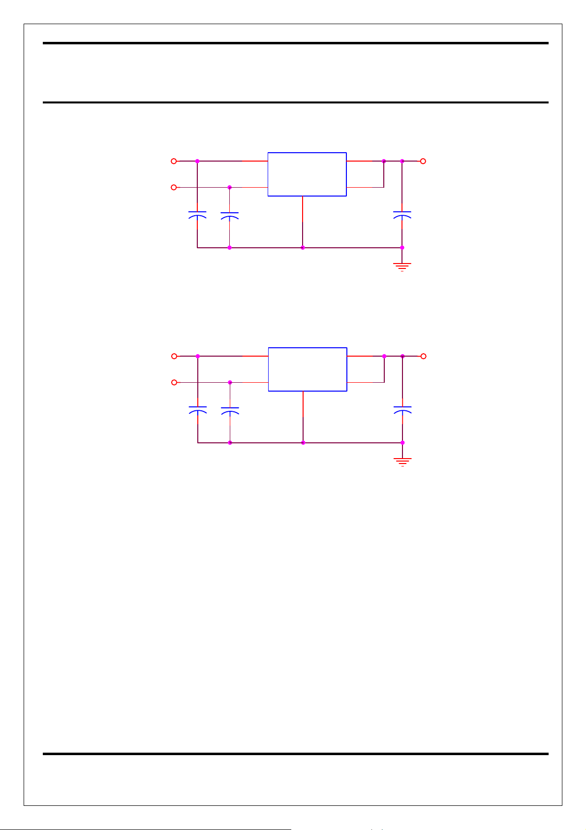
Fixed Output Parts
Dual Input Ultra Low Dropout
Voltage Regulator (ULDO)
L1581X-2.5
Vin
Vctrl
C1
330uF
C2
10uF
4
CTR'L
OUTVin
SENSE
ADJ
2
L1581 Series
TO-252
35
2.5V Vout
1
C4
330uF
L1581X-3.3
Vin
Vctrl
C1
330uF
C2
10uF
4
CTR'L
2
SENSE
ADJ
35
OUTVin
1
3.3V Vout
C4
330uF
NOTES :
(1) If the same voltage is input to both INPUT and CONTROL, then the dropout voltage will become 1.3V
maximum.
(2) A small (~0.033uF) capacitor can be used to bypass the ADJUST pin to improve transient response, if needed.
(3) Capacitor values are for reference only. Good quality, low ESR tantalum or aluminum electrolytic capacitors
should be used. Increasing the value of the output capacitor will improve the overall transient response.
2
OCT-11-Y02
Page 3

NIKO-SEM
Dual Input Ultra Low Dropout
Voltage Regulator (ULDO)
ABSOLUTE MAXIMUM RATINGS
L1581 Series
TO-252
z Input Supply Voltage, V
Control Input Voltage, V
z Power Dissipation, PD
z Thermal Resistance
Junction to Case, θJC
z Thermal Resistance
IN
CTRL
13.2V
Internally
60 °C/W
7V
Limited
3 °C/W
z Operating Junction
Temperature Range, TJ
z Storage Temperature
Range, T
z Lead Temperature, T
STG
LEAD
(Soldering, 10 Seconds)
Junction to Ambient, θJA
ELECTRICAL CHARACTERISTICS (
C
= Cin= C
ctl
out
=10
,TJ = 25 °C)
uF
Unless otherwise specified, V
Parameter Symbol Test Conditions Typical Limits
Reference Voltage
(Adj. Voltage
Versions)
Dropout Voltage
(1) (2)
(1)
V
REF
VI - VO
V
=4.5V, VIN=2.05V, I
CTRL
=10mA 1.237V~1.263V
OUT
V
V
CTRL
= 4.5V, 10mA <
CTRL
VIN = 2.05V
= 4.75V, I
OUT
= 5A
I
OUT
< 5A,
Minimum VIN
Output Voltage
(Fixed Voltage
(1)
V
Versions)
Line Regulation
(1)
REG
Load Regulation REG
(6)
Thermal Regulation
REG
OUT
(LINE)
(LOAD)
(Thermal)
V
V
V
CTRL
0.8V) to 5.5V, I
V
CTRL
I
OUT
0.002
= 5V, V
CTRL
= 5V, 10mA <
CTRL
V
IN
I
OUT
= V
= V
IN
=10mA
OUT
OUT
+ 0.8V
= 4.5V to 12V, VIN = (V
= 10mA
OUT
= 4.5V, VIN = (V
= 10mA ~ 5A
+ 0.8V,
< 5A,
I
OUT
+0.8V) ,
OUT
OUT
+
= V
out
1.25V
1.231V~1.269V
0.54V 0.62V (Max)
V
OUT
1.0mV 3.0mV
1.0mV 5.0mV
0 to 125 °C
-40 to 150 °C
, V
sns
= 0V ,
adj
± 1%
± 1.5%
0.02% / W
260 °C
Minimum Load
Current
(4)
Adjust Pin Current I
Control Pin Current
(3)
IO
ADJ
I
CTRL
Current Limit ICL
% / W
V
V
I
V
I
V
Δ
= 5V, VIN = V
CTRL
= 4.5V, VIN =
CTRL
= 10mA
OUT
= 4.5V, VIN =
CTRL
= 5A
OUT
= 4.5V, VIN =
CTRL
V
OUT
= 100mV
+0.8V
OUT
V
V
V
OUT
OUT
OUT
+0.8V
+0.8V
+0.8V
,
,
3
5mA 10mA
50µA 120µA
33mA 120mA
5.1A (Min)
OCT-11-Y02
Page 4

NIKO-SEM
Ripple Rejection
(5)
Ratio
Dual Input Ultra Low Dropout
Voltage Regulator (ULDO)
R
V
A
= VIN = 5V, I
CTRL
OUT
= 5A
L1581 Series
TO-252
80dB 60dB (Min)
NOTE :
(1) Low duty cycle pulse testing with Kelvin connections required.
(2) Minimum input to output voltage differential required to maintain 1% regulation.
(3) Current used to drive the output section.
(4) Required to maintain regulation. Resistor divider R1, R2 is usually utilized for minimum load current.
(5) V
(6)
RIPPLE
30ms.
= 1V
PK-PK
, 120Hz.
DEVICE SELECTION GUIDE
Device
Package
Marking
PIN CONFIGURATIONS
L1581D L1581D-2.5 L1581D-3.3
TO-252 TO-252 TO-252
L1581D L1581D-2.5 L1581D-3.3
54
21
3
Pin # Function
1 Sense
2 Adjust
3 Output
4 Control
5 Input
Note: TAB is Output Pin
4
OCT-11-Y02
Page 5

NIKO-SEM
PIN FUNCTIONS
Dual Input Ultra Low Dropout
Voltage Regulator (ULDO)
NO FUNCTION DESCRIPTION
L1581 Series
TO-252
1 Sense
2
Adjust
3 Output
4 Control
5 Input
This pin is the positive side of the reference voltage for the device. With
this pin it is possible to Kelvin sense the output voltage at the load.
This pin is the negative side of the reference voltage for the device.
Transient response can be improved by adding a small bypass capacitor
from the adjust pin to ground.
This is the power output of the device, and is electrically connected to
the TAB.
This pin is the supply pin for the control circuitry for the device. The
current flow into this pin will be approximately 1% of the output. For the
device to regulate, the voltage at this pin must be between 1.0V and
1.3V greater than the output voltage (see dropout specifications).
This is the collector input to the power device of the L1581. The output
load current is supplied through this pin. For the device to regulate, the
voltage on this pin must be between 0.1V and 0.7V greater than the
output, depending upon load current (see dropout specifications).
5
OCT-11-Y02
Page 6

NIKO-SEM
Dual Input Ultra Low Dropout
Voltage Regulator (ULDO)
L1581 Series
TO-252
TO-252 (DPAK) MECHANICAL DATA
mm mm
Dimension
Min. Typ. Max.
Dimension
Min. Typ. Max.
A 9.7 H 0.89 2.03
B 2.19 2.38 I 6.35 6.73
C 0.46 0.58 J 5.21 5.46
D 0.89 1.27 K
E 0.46 0.53 L 0.64 0.89
F 0.00 0.13 M 1.27BSC
G 3.04 5.33 N
5
4
3
2
1
6
OCT-11-Y02
 Loading...