

Page 1
NIKO-SEM
5A Adjustable Low Dropout
Linear Regulator (LDO)
GENERAL DESCRIPTION
FEATURES
L1084S5
TO-263
The L1084 is a positive and low dropout
three-terminal voltage regulator with 5A output current capability. This device is designed for use in low voltage applications that
offers lower dropout voltage and faster transient response.
This device is fully protected against over
current faults, over temperature operation,
reversed input polarity, reversed lead insertion, transient voltage spike …etc.
On-Chips trimming the reference voltage to
1% and features the low dropout of maximum 1.45 volts.
The L1084 Series regulators are available
in the popular industry standard TO-263
packages.
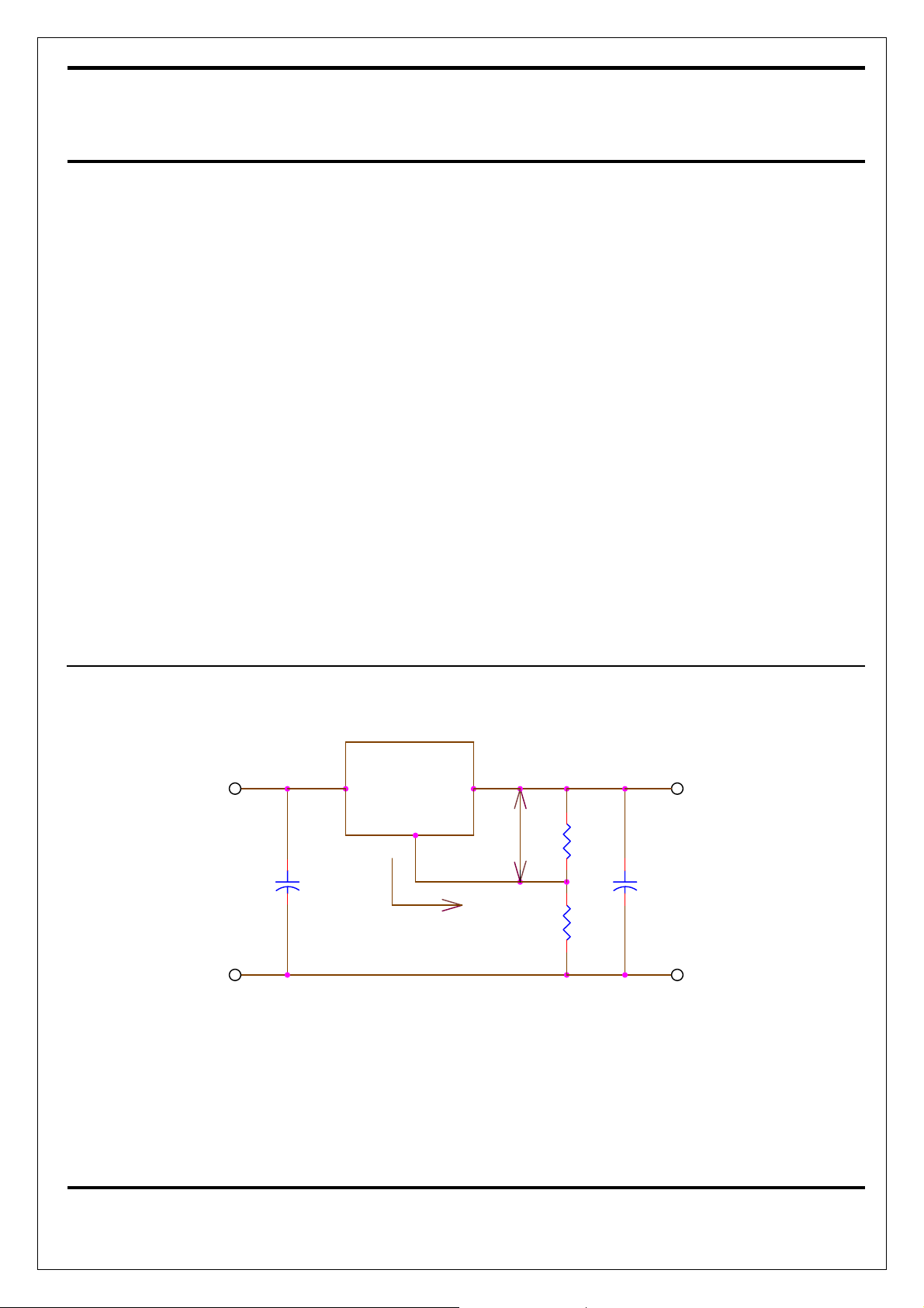
TYPICAL APPLICATION
Very easy to use, it requires only two
z
external resistors to set the output voltage
Low dropout voltage:
z
1.2V typical at up to 5A
Low ground current
z
Fast transient response
z
Current & thermal lim iting
z
Line regulation: 0.5% typical
z
Load regulation: 0.5% typical
z
TO-263 packages
z
APPLICATIONS
High current microprocessor supplies
z
Low voltage logic supply
z
Powering VGA & sound card
z
Portable instrumentation
z
Constant current regulator
z
z
zz
Post regulator for switching power supply
z
Vin
5 3
L1084X5
OUTIN
Vout
Cin
10uF
+
ADJ
Iadj
Vref
2
R1
R2
Cout
+
10uF
Vo = Vref (1+R2/R1) + Iadj x R2
1. Cin needed if device is far from filter capacitors.
2. Cout required for stability.
- Basic Adjustable Regulator Circuit -
1
Rev. 1.0 MAR
Page 2
NIKO-SEM
5A Adjustable Low Dropout
Linear Regulator (LDO)
ABSOLUTE MAXIMUM RATINGS
L1084S5
TO-263
Maximum Supply Voltage 7V
z
Power Dissipation
z
Thermal Resistance
z
Junction to Case,
Thermal Resistance
z
θ
JC
Junction to Ambient,
TO-263
θ
JA
Internally
Limited
2.5 °C/W
60 °C/W
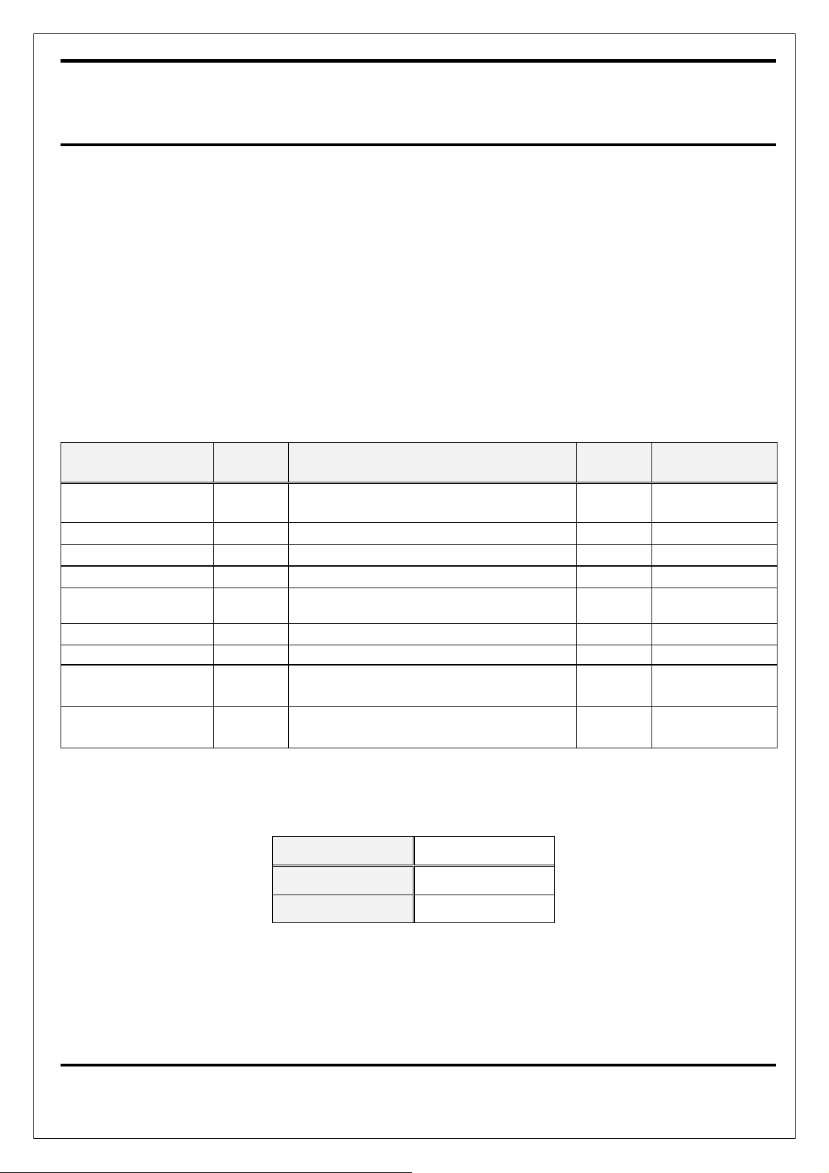
ELECTRICAL CHARACTERISTICS
Parameter
Symbol
Reference Voltage V
Dropout Voltage VD
Line Regulation REG
Load Regulation REG
Minimum Load
Current
Adjust Pin Current I
Current Limit ICL VIN - V
RMS Output Noise VN
Ripple Rejection
Ratio
VIN = 5V, I
REF
Δ
(V
(LINE)
(V
(LOAD)
IO
ADJ
1.5V ≤ (V
0.003%
f = 120Hz, C
R
A
VIN = 5V, I
V
= 1%, I
REF
+ 1.5V) ≤ V
OUT
IN -VOUT
OUT
Test Conditions Typical Limits
OUT
) = 3V, 10mA ≤ I
IN -VOUT
= 2V 7.5A 5.0A (Min)
OUT
Operating Junction
z
Temperature Range
Storage Temperature
z
Range
Lead Temperature
z
(Soldering, 10 Seconds)
(
Unless otherwise specified, TA = 25 °C.)
= 10mA
= 5A
OUT
≤
IN
) ≤ 5.75V
7V, I
= 10mA
OUT
≤ 5A
OUT
1.25V
1.2V 1.45V
0.5% 2%
0.5% 2.5%
10mA
55µA 100µA
OUT
= 22µF for ADJ pin,
ADJ
= 5A
of V
72dB 60dB (Min)
0 to 125 °C
-40 to 150 °C
260 °C
1.23V
1.27V
Min
Max
DEVICE SELECTION GUIDE
Package
Marking
Device
L1084S5
TO-263 (5-Lead)
L1084S5
2
Rev. 1.0 MAR
Page 3
NIKO-SEM
5A Adjustable Low Dropout
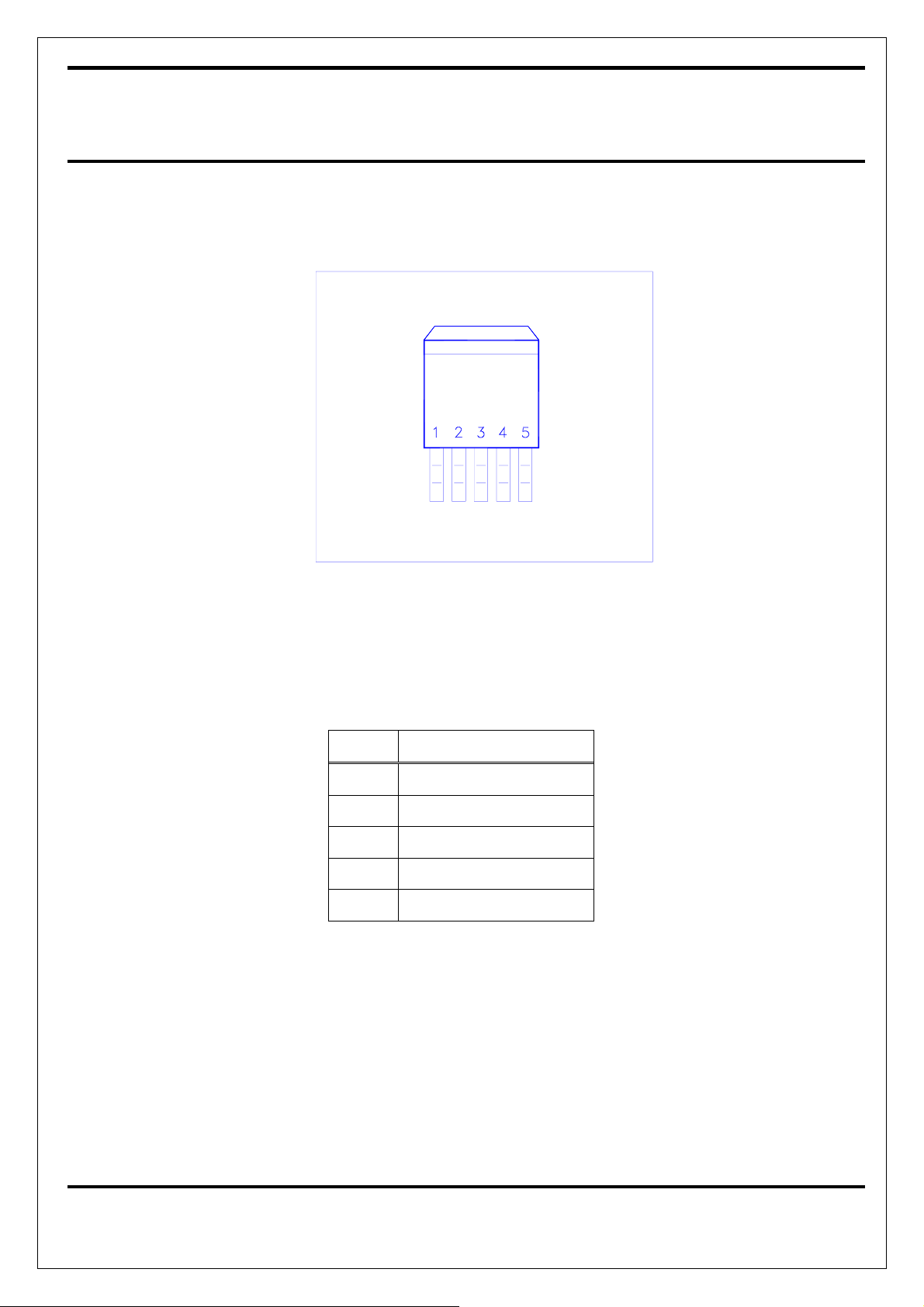
PIN CONFIGURATIONS
Linear Regulator (LDO)
L1084S5
TO-263
Pin # Function
1 NC
2 Adjust
3 Output
4 NC
5 Input
Note: TAB is Output Pin
3
Rev. 1.0 MAR
Page 4
NIKO-SEM
5A Adjustable Low Dropout
Linear Regulator (LDO)
L1084S5
TO-263
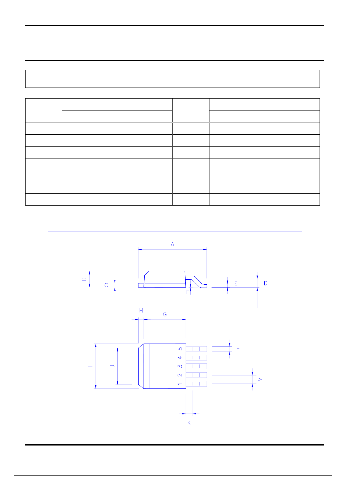
TO-263 (D2PAK, 5-Lead) MECHANICAL DATA
Dimension
mm
Dimension
Min. Typ. Max.
Min. Typ. Max.
mm
A 14.5 15 15.8 H 1.0 1.5 1.8
B 4.2 4.7 I 9.8 10.3
C 1.20 1.35 J 6.5
D 2.8 K 1.5
E 0.3 0.4 0.5 L 0.7 0.85 1.0
F -0.102 0.203 M 1.57 1.7 1.83
G 8.5 9 9.5 N
4
Rev. 1.0 MAR
 Loading...