

Page 1
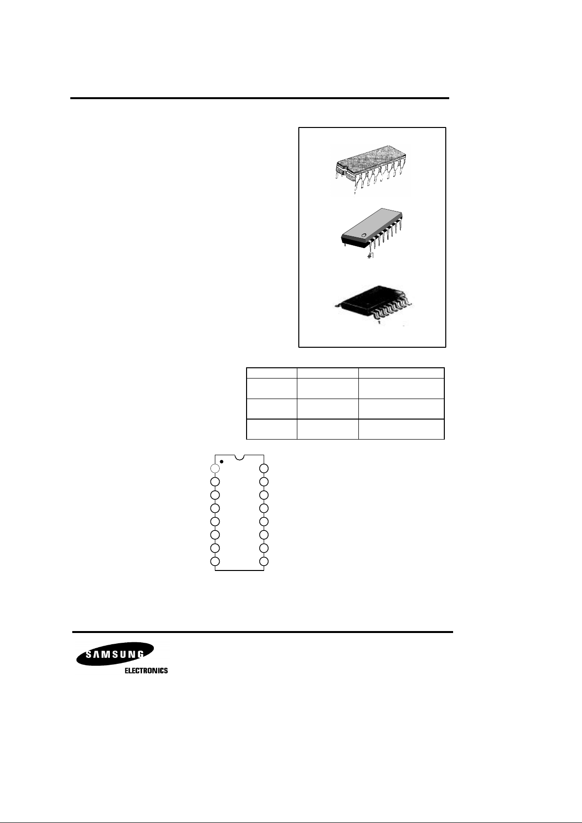
KT8554B/7B 1 CHIP CODECS
INTRODUCTION
The KT8554B/7B are single-chip PCM encoders and decoders
(PCM CODECs) and PCM line filters. These devices provide
all the functions required to interface a full-duplex voice
telephone circuit with a time-division-multiplex (TDM)
system.
These devices are designed to perform the transmit encoding
and receive decoding as well as the transmit and receive filtering functions in PCM system. They are intended to be used
at the analog termination of a PCM line or trunk.
These devices provide the bandpass filtering of the analog
signals prior to encoding and after decoding. These combination devices perform the encoding and decoding of voice and
call progress tones as well as the signalling and supervision
information.
FEATURES
• Complete CODEC and filtering system
• Meets or exceeds AT&T D3/D4 and CCITT
specifications
µ-Law : KT8554B, A-Law : KT8557B
• On-chip auto zero, sample and hold, and precision
voltage references
• Low power dissipation : 60mW (operating)
3mW (standby)
• ± 5V operation
• TTL or CMOS compatible
• Automatic power down
PIN CONFIGURATION
Fig. 1
Device Package Operating Temperature
KT8554BJ
KT8557BJ
16-CERDIP
- 25 ~ 125°C
KT8557BN
KT8554BN
16-DIP-300A
- 25 ~ 70°C
KT8554BD
KT8557BD
16-SOP-BD300
-SG
- 25 ~ 70°C
VFXI
+
VFXI
-
GS
X
TS
X
FSXS
D
X
BCLK
X
MCLK
X
V
BB
GNDA
VFRO
V
CC
FS
R
D
R
BCLKR/CLKSEL
MCLKR/PDN
1
2
3
4
5
6
7
8
16
15
14
13
12
11
10
9
KT8554B/7B
ORDERING INFORMATION
16-CERDIP
16-DIP-
16-SOP-BD300
-SG
Page 2

KT8554B/7B 1 CHIP CODECS
PIN DESCRIPTION
ABSOLUTE MAXIMUM RATINGS (Ta = 25
o
C)
Pin No Symbol Description
1 V
BB
VBB = - 5V ±5%.
2 GNDA Analog ground.
3 VFRO Analog output of the receive power Amp.
4 V
CC
V
CC
= +5V ± 5%.
5 FS
R
Receive frame sync pulse. 8KHz pulse train.
6 D
R
PCM data input.
7
Logic input which selects either 1.536MHz/1.544MHz or 2.048MHz for master
clock in normal operation and BCLKX is used for both TX and RX directions.
Alternately direct clock input available, very from 64KHz to 2.048MHz.
8
When MCLKR is connected continuously high, the device is powered down.
Normally connected continusously low, MCLKX is selected for all DAC timing.
Alternately direct 1.536MHz/1.544MHz or 2.048MHz clock input available.
9 MCLK
X
Must be1.536MHz/1.544MHz or 2.048MHz.
May be vary from 64KHz to 2.048MHz but BCLKX is externally tied with MCLK
X
in normal operation.
11 D
X
PCM data output.
12 FS
X
TX frame sync pulse. 8KHz pulse train.
13 TS
X
Changed from high to low during the encoder timeslot. Open drain output.
Analog output of the TX input amplifier.
Used to set gain through external resistor.
15 VFXI
-
Inverting input stage of the TX analog signal.
16 VFXI
+
Non-inverting input stage of the TX analog signal.
Characteristic Symbol Value Unit
Positive Supply Voltage
V
CC
7 V
Negative Supply Voltage V
BB
- 7 V
Voltage at Any Analog Input or Output V
I (A)
V
CC
+ 0.3 to V
BB
- 0.3 V
Voltage at Any Digital Input or Output Vl
(D)
V
CC
+ 0.3 to GNDA - 0.3 V
Operating Temperature Range Ta - 25 to + 125
o
C
Storage Temperature Range T
STG
- 65 to + 150
o
C
Lead Temperature (Soldering, 10 secs) T
LEAD
300
o
C
10
BCLK
X
BCLKR /
CLKSEL
MCLKR /
PDN
GS
X
14
Page 3
KT8554B/7B 1 CHIP CODECS
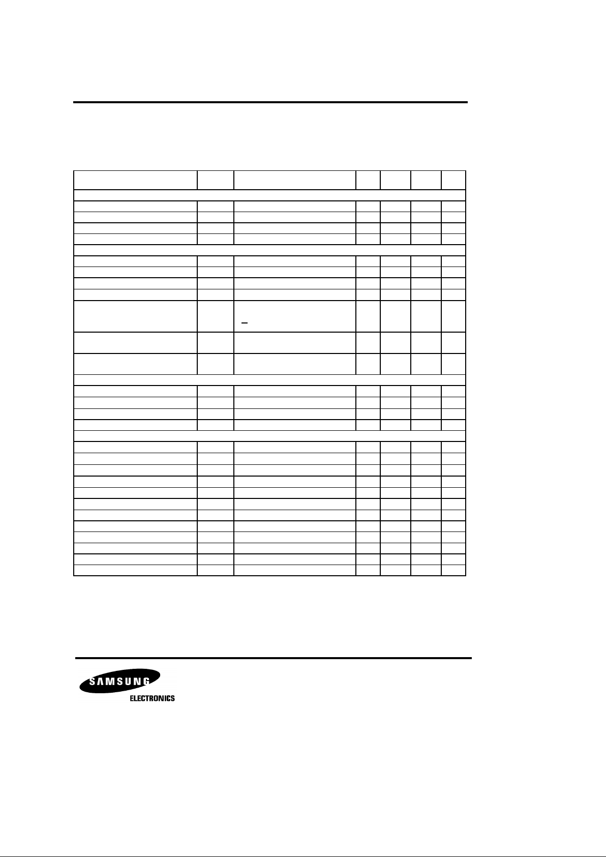
ELECTRICAL CHARACTERISTICS
(Unless otherwise noted, VCC = 5.0V ±5%, VBB = - 5.0V ±5%, GNDA = 0V, Ta = 0 oC to 70 oC ; typical characteristics
specified at V
CC
= 5.0V, V
BB
= - 5.0V, Ta = 25 oC ; all signals referenced to GNDA).
Characteristic Symbol Test Conditions Min Typ Max Unit
Power Dissipation
Power-Down Current I
CC (DOWN)
No Load 0.5 1.5 mA
Power-Down Current I
BB (DOWN)
No Load 0.05 0.3 mA
Active Current I
CC (A)
No Load 6.0 9.0 mA
Active Current I
BB (A)
No Load 6.0 9.0 mA
Digital Interface
Input Low Voltage V
IL
0.6 V
Input High Voltage V
IH
2.2 V
Input Low Current I
IL
GNDA ≤ VIN≤VIL, all digital inputs
-10 10
µA
Input High Current I
IH
V
IH
≤ V
IN
≤ V
CC
-10 10
µA
Output Low Voltage V
OL
DX,IL = 3.2mA
SIGR, IL = 1.0mA
TSX, IL = 3.2mA,open drain
0.4
0.4
0.4
V
V
V
DX, IH = -3.2mA
SIGR, IH = -1.0 mA
2.4
2.4
V
V
Output Current in High Impedance
State (TRI-STATE)
I
O (HZ)
DX, GNDA ≤ V
O
≤ V
CC
-10 10
µA
Analog Interface with Receive Filter
Output Resistance R
O
Pin VFRO 1 3
Ω
Load Resistance R
L
VFRO = ±2.5V
600
Ω
Load Capacitance C
L
500 pF
Output DC Offset Voltage V
OO (RX)
-200 200 mV
Analog Interface with Transmit input Amplifier
Input Leakage Current I
LKG
-2.5V≤V≤+2.5V, VFXI + or VFXI -
-200 200 nA
Input Resistance R
I
-2.5V≤V≤+2.5V, VFXI + or VFXI -
10
MΩ
Output Resistance R
O
Closed loop, unity gain 1 3
Ω
Load Resistance R
L
GS
X
10
KΩ
Load Capacitance C
L
GS
X
50 pF
Output Dynamic Range V
OD (TX)
GSX, RL≤10KW ±2.8
V
Voltage Gain G
V
VFXI + to GS
X
5,000 V/V
Unity Gain Bandwidth BW 1 2 MHz
Offset Voltage V
IO (TX)
-20 20 mV
Common-Mode Voltage V
CM (TX)
CMRRXA > 60dB -2.5 2.5 V
Common-Mode Rejection Ratio CMRR DC Test 60 dB
Power Supply Rejection Ratio PSRR DC Test 60 dB
Output High Voltage
V
OH
Page 4
KT8554B/7B 1 CHIP CODECS
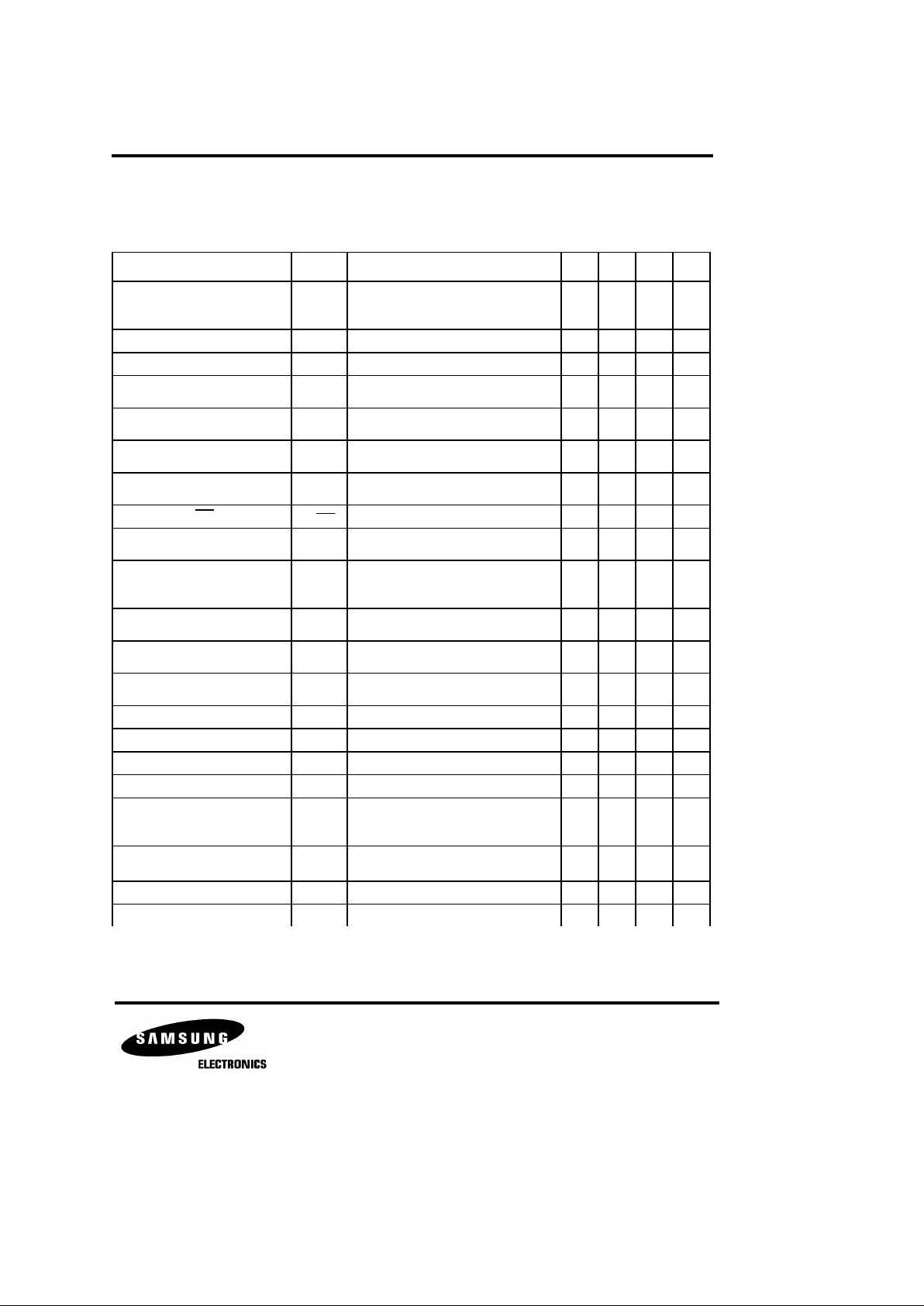
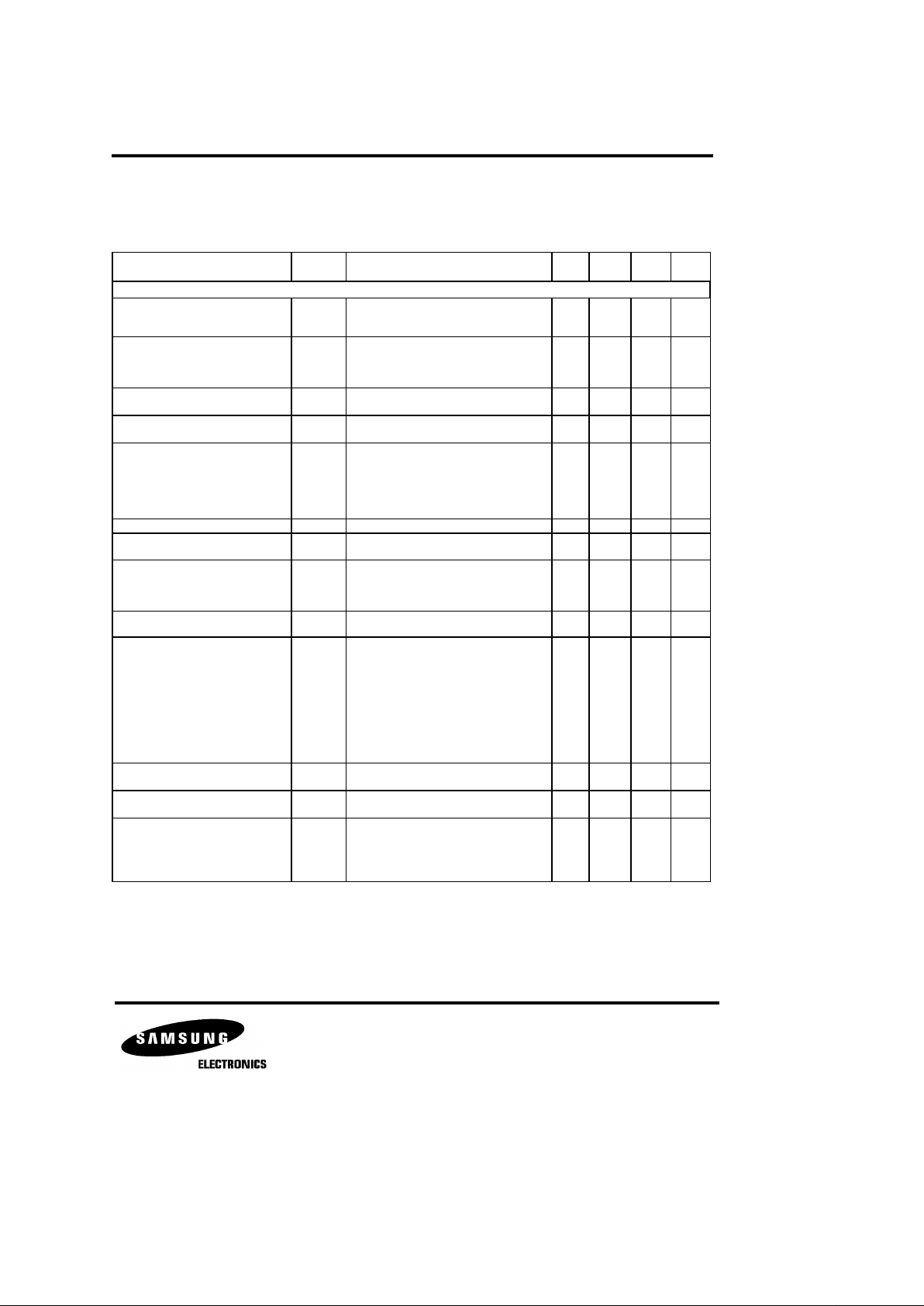
TIMING CHARACTERISTICS
(Unless otherwise noted, V
CC
= 5.0 ±5%, V
BB
= -5.0V ±5%, GNDA = 0V, Ta = 0oC to 70 oC; typical characteristics
specified at V
CC
= 5.0V, V
BB
= -5.0V, Ta = 25 oC; all signals referenced to GNDA.)
Characteristic Symbol Test Conditions Min Typ Max Unit
Frequency of Master Clocks f
MCK
Depends on the device used and the
BCLKR /CLKSEL Pin.
MCLKX and MCLK
R
1.536
1.544
2.048
MHz
MHz
MHz
Rise Time of Bit Clock t
R (BCK) tPB
= 488ns 50 ns
Fall Time of Bit Clock t
F (BCK) tPB
= 488ns 50 ns
Holding Time from Bit Clock
Low to Frame Sync
0 ns
Holding Time from Bit Clock
High to Frame Sync
0 ns
Set-Up Time from Frame Sync
to Bit Clock Low
80 ns
Delay Time from BCLKX High
to Data Valid
0 180 ns
Delay Time to TSX Low tD
(TSXL)
Load = 150pF plus 2 LSTTL loads 140 ns
Delay Time from BCLKX Low to
Data Output Disabled
50 165 ns
Delay Time to Valid Data from
FSX or BCLKX, Whichever
Comes Later
t
D (VD)
CL = 0pF to 150pF 20 165 ns
Set-Up Time from DR Valid to
BCLK
R/X
Low
50 ns
Hold Time from BCLK
R/X
Low
to DR Invalid
50 ns
Set-Up Time from FS
X/R
to
BCLK
X/R
Low
Short frame sync pulse (1 or 2 bit
clock periods long) (Note1)
50 ns
Width of Master Clock High t
W (MCKH)
MCLKX and MCLK
R
160 ns
Width of Master Clock Low t
W (MCKL)
MCLKX and MCLK
R
160 ns
Rise Time of Master Clock t
R (MCK)
MCLKX and MCLK
R
50 ns
Fall Time of Master Clock t
F( MCK)
MCLKX and MCLK
R
50 ns
Set-Up Time from BCLKX High
(and FSX In Long Frame Sync
Mode) to MCLKX Falling Edge
t
SU (BHMF)
Period of Bit Clock t
CK
485 488 15,725ns
Width of Bit Clock High t
W (BCKH) VIH
= 2.2V 160 ns
Width of Bit Clock Low t
W (BCKL) VIL
= 0.6V 160 ns
t
H (LFS)
t
H (HFS)
t
SU (FBCL)
t
D (HDV)
t
D (LDD)
t
SU (DR BL)
t
H (BL DR)
t
SU (FBLS)
Long frame only
Short frame only
Long frame only
Load = 150pF plus 2 LSTTL loads
First bit clock after the leading
edge of FS
X
Page 5
KT8554B/7B 1 CHIP CODECS
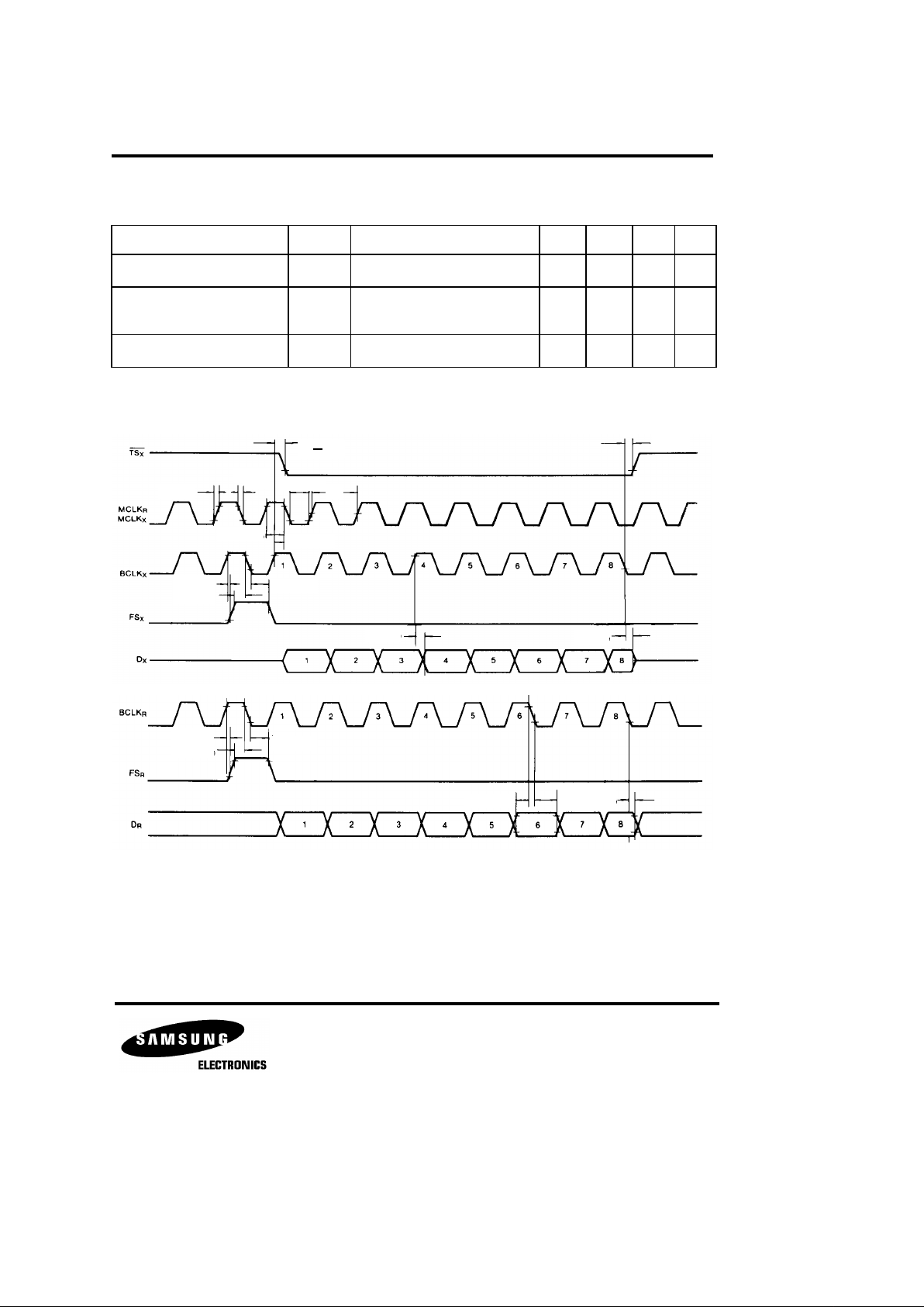
TIMING CHARACTERISTICS (Continued)
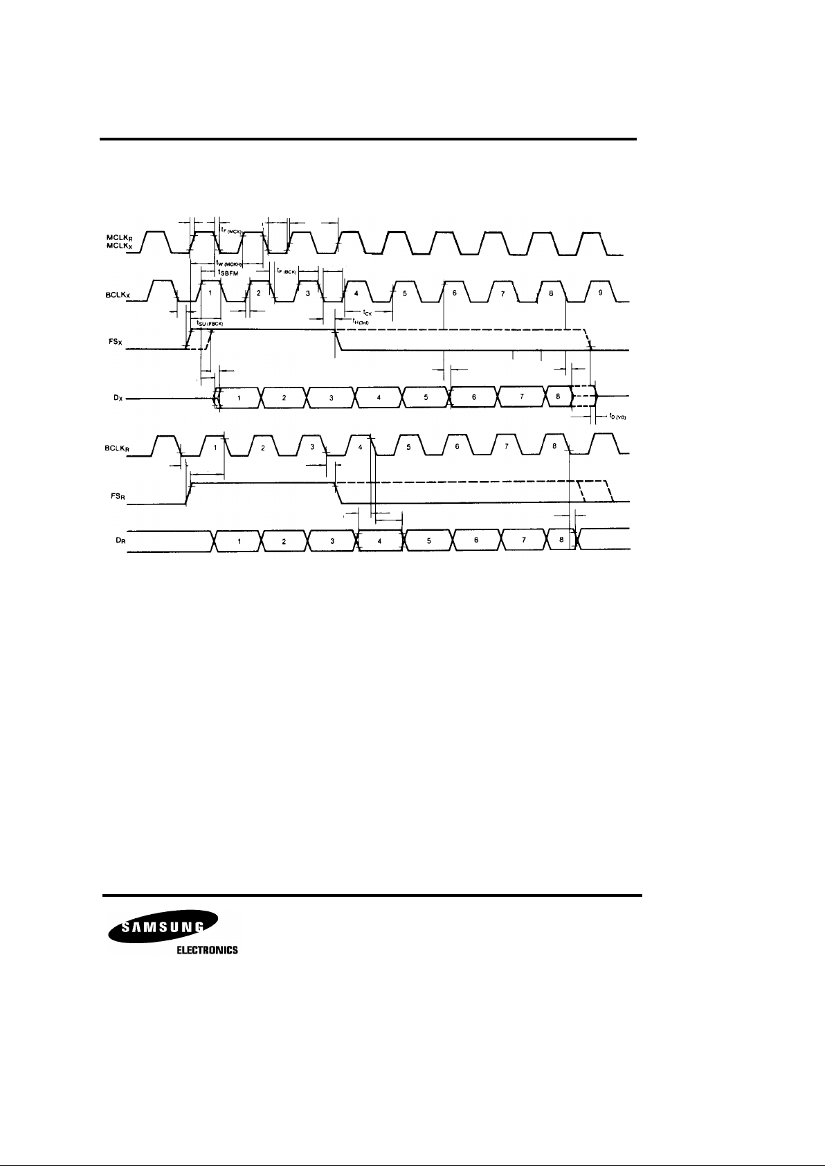
Note 1 : For short frame sync timing, FSX and FS
R
must go high while their respective bit clocks are high.
TIMING DIAGRAM
Fig. 2. Short Frame Sync Timing
Characteristic Symbol Test Conditions Min Typ Max Unit
Hold Time from BCLK
X/R
Low
to FS
X/R
Low
Short frame sync pulse (1 or 2 bit
clock periods long) (Note 1)
Hold Time from 3rd Period of
Bit Clock Low to Frame Sync
(FSX or FSR)
t
H (3rd )
Long frame sync pulse (from 3 to
8 bit clock periods long)
100 ns
Minimum Width of the Frame
Sync Pulse (Low Level)
t
H (BLFL)
t
WFL
64K bit/s operating mode
100
160
ns
ns
t
D (LDD)
t
D (TS X L)
t
H (BLDR)
t
H (BLDR)
t
SU (DR BL)
t
H (BLFL)
t
H (HFS)
t
SU (FBCL)
t
D (LDD)
t
D (HDV)tSU (BHMF)
t
H (HFS)
t
SU (FBLS)
t
H (BLFL)tW (MCKH)tCKtW (MCKL)tF (MCK)tR (MCK)
Page 6
KT8554B/7B 1 CHIP CODECS
TIMING DIAGRAM (Continued)
Fig. 3 Long Frame Sync Timing
t
W (BCKH) tW (BCKL)
t
R (MCK)
t
W (MCKL)
t
CK
t
H (BL DR)
t
H (BL DR)
t
SU (DR BL)
t
H (3rd)
t
SU(FBCK)
t
H (HFS)
t
D (LDD)
t
D (HDV)
t
D (VD)
t
D (VD)
t
H (HFS)
t
RB
t
SU (BHMF)
Page 7
KT8554B/7B 1 CHIP CODECS
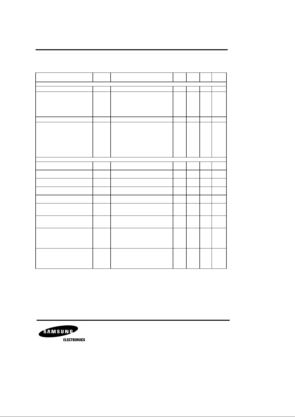
TRANSMISSION CHARACTERISTICS
(Unless otherwise specified : Ta = 0oC to 70 oC, VCC = 5V ±5%, VBB = -5V ±5%, GNDA = 0V, f = 1.02KHz,
VIN = 0dBm0, transmit input amplifier connected for unity-gain non-inverting.)
Characteristic Symbol Test Conditions Min Typ Max Unit
Amplitude Respons
Receive Gain, Absolute G
V (ARX)
Ta = 25 oC, V
CC
= 5V, V
BB
= -5V
Input = Digital code sequence for
0dBm0 signal at 1020Hz
-0.15 0.15 dB
Receive Gain, Relative to G
V (ARX)
G
V (RRX)
f = 0Hz to 3000Hz
f = 3300Hz
f = 3400Hz
f = 4000Hz
-0.15
-0.35
-0.7
0.15
0.05
0
-14
dB
dB
dB
dB
Absolute Receive Gain Variation
with Temperature
∆G
V (ARX)
/∆T
Ta = 0 oC to 70 oC
±0.1
dB
Absolute Receive Gain Variation
with Supply Voltage
∆G
V (ARX)
/∆V
V
CC
= 5V ±5%, V
BB
= -5V ±5% ±0.05
dB
Receive Gain Variations with
Level
∆G
V (RXL)
Sinusoidal test method ; reference
input PCM code corresponds to an
Ideally encoded -10dBm0 signal
PCM level = -40dBm0 to +3dBm0
PCM level = -50dBm0 to -40dBm0
PCM level = -55dBm0 to -50dBm0
-0.2
-0.4
-1.2
0.2
0.4
1.2
dB
dB
dB
Receive Output Drive Level V
O (RX)
RL = 600Ω
-2.5 2.5 V
Absolute Levels V
AL
Nominal 0dBm0 level is 4dBm (600Ω)
0dBm0
1.2276 V
rms
Max overload level (3.17dBm0):
KT8554B
Max overload level (3.14dBm0):
KT8557B
2.501 V
PK
Ta = 25 oC, VCC = 5V, VBB = -5V
Input at GSX = 0dBm0 at 1020Hz
-0.15 0.15 dB
Transmit Gain, Relative to G
V (ATX)
G
V (RTX)
f = 16Hz
f = 50Hz
f = 60Hz
f = 200Hz
f = 300Hz - 3000Hz
f = 3300Hz
f = 3400Hz
f = 4000Hz
f = 4600Hz and up, measure
response from 0Hz to 4000Hz
-1.8
-0.15
-0.35
-0.7
-40
-30
-26
-0.1
0.15
0.05
0
-14
-32
dB
dB
dB
dB
dB
dB
dB
dB
dB
Absolute Transmit Gain Variation
with Temperature
∆G
V(ATX)
/∆T
Ta = 0 oC to 70 oC
±0.1
dB
Absolute Transmit Gain Variation
with Supply Voltage
∆G
V (ATX)
/∆V
VCC = 5V ±5%, VBB = -5V ±5%
±0.05
dB
Sinusoldal test method
Reference level = - 10dBm0
VFXI + = - 40dBm0 to + 3dBm0
VFXI + = - 50dBm0 to - 40dBm0
VFXI + = - 55dBm0 to - 50dBm0
- 0.2
- 0.4
- 1.2
0.2
0.4
1.2
dB
dB
dB
Transmit Gain, Absolute G
V (ATX)
Max Overload Level
V
OL (MAX)
∆
G
V (TXL)
Transmit Gain Variations with
Level
Page 8
KT8554B/7B 1 CHIP CODECS
TRANSMISSION CHARACTERISTICS (Continued)
Characteristic Symbol Test Conditions Min Typ Max Unit
Envelope Delay Distortion with Frequency
Receive Delay, Absolute t
D (ARX)
f = 1600Hz 180 200
µs
Receive Delay, Relative to t
D (ARX)
t
D (RRX)
f = 500Hz - 1000Hz
f = 1000Hz - 1600Hz
f = 1600Hz - 2600Hz
f = 2600Hz - 2800Hz
f = 2800Hz - 3000Hz
-40
-30
-25
-20
70
100
145
90
125
175
µs
µs
µs
µs
µs
Transmit Delay, Absolute t
D (ATX)
f = 1600Hz 290 315
µs
Transmit Delay, Relative to t
D (ATX)
t
D (RTX)
f = 500Hz - 600Hz
f = 600Hz - 800Hz
f = 800Hz - 1000Hz
f = 1000Hz - 1600Hz
f = 1600Hz - 2600Hz
f = 2600Hz - 2800Hz
f = 2800Hz - 3000Hz
195
120
50
20
55
80
130
220
145
75
40
75
105
155
µs
µs
µs
µs
µs
µs
µs
Noise
Receive Noise, C Message
Weighted
N
RXC
PCM code equals alternating
positive and negative zero, KT8554B
8 11 dBrnc0
Receive Noise, P Message
Weighted
N
RXP
PCM code equals, positive zero,
KT8557B
-82 -79 dBm0p
Transmit Noise, C Message
Weighted
N
TXC
KT8554B
12 15 dBrnc0
Transmit Noise, P Message
Weighted
N
TXP
KT8557B
74 -67 dBm0p
Noise, Single Frequency N
SF
f = 0KHz to 100KHz, loop around
measurement, VFXI + = 0V
rms
-53 dBm0
Positive Power Supply Rejection,
Transmit
PSRR
(PTX)
VFXI + = 0V
rms
,
VCC = 5.0V
DC
+ 100mV
rms
f = 0KHz - 50KHz
40 dBC
Negative Power Supply Rejection,
Transmit
PSRR
(NTX)
VFXI + = 0V
rms
,
V
BB
= -5.0VDC + 100mV
rms
f = 0KHz - 50KHz
40 dBC
Positive Power Supply Rejection,
Receive
PSRR
(PRX)
PCM code equals positive zero
V
CC
= 5.0VDC + 100mV
rms
f = 0Hz - 4000Hz
f = 4KHz - 25KHz
f = 25KHz - 50KHz
40
40
36
dBC
dB
dB
Negative Power Supply Rejection,
Receive
PSRR
(NRX)
PCM code equals positive zero
V
BB
= 5.0VDC + 100mV
rms
f = 0Hz - 4000Hz
f = 4KHz - 25KHz
f = 25KHz - 50KHz
40
40
36
dBC
dB
dB
Page 9
KT8554B/7B CMOS INTEGRATED CIRCUIT
TRANSMISSION CHARACTERISTICS (Continued)
Note 1. CT
(RX-TX)
is measured with a - 40dBm0 activating signal applied at VFXI +
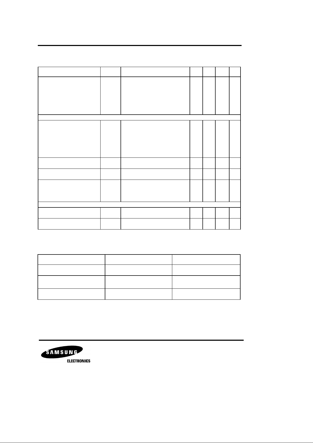
ENCODING FORMAT AT Dx OUTPUT
Characteristic Symbol Test Conditions Min typ Max Unit
Spurious Out-of-Band Signals
at the Channel Output
SOS
Loop around measurement, 0dBm0,
300Hz - 3400Hz input PCM applied to
DR, Measure individual image
signals at VFRO
4600Hz - 760Hz
7600Hz - 8400Hz
8400Hz - 100,000Hz
-32
-40
-32
dB
dB
dB
Distortion
Signal to Total Distortion
Transmit or Receive
Half-Channel
THD
TX
THD
RX
Sinusoidal test method
Level = 3.0dBm0
= 0dBm0 to 30dBm0
= -40dBm0 XMT
RCV
= -55dBm0 XMT
RCV
33
26
29
30
14
15
dBC
dBC
dBC
dBC
dBC
dBC
Single Frequency Distortion,
Transmit
-46 dB
Single Frequency Distortion,
Receive
-46 dB
Intermodulation Distortion THD
IMD
Loop around measurement,
VFXI + = -4dBm0 to -21dBm0, two
frequencies in the range
300Hz - 3400Hz
-41 dB
Crosstalk
Transmit to Receive Crosstalk,
0dBm0 Transmit Level
f = 300Hz - 3400Hz
DR = Steady PCM code
-90 -75 dB
Receive to Transmit Crosstalk,
0dBm0 Receive Level
-90 -70
(Note1)
dB
µ
-Law KT8554B
A-Law KT8557B
VIN (at GSX) = + Full Scale 1 0 0 0 0 0 0 0 1 0 1 0 1 0 1 0
1 1 1 1 1 1 1 1
0 1 1 1 1 1 1 1
1 1 0 1 0 1 0 1
0 1 0 1 0 1 0 1
VIN (at GSX) = - Full Scale 0 0 0 0 0 0 0 0 0 0 1 0 1 0 1 0
THD
SF (TX)
THD
SF (RX)
CT
(TX-RX)
CT
(RX-TX)
f = 300Hz - 3400Hz, VFXI = 0V
VIN (at GSX) = 0V
Page 10
KT8554B/7B CMOS INTEGRATED CIRCUIT
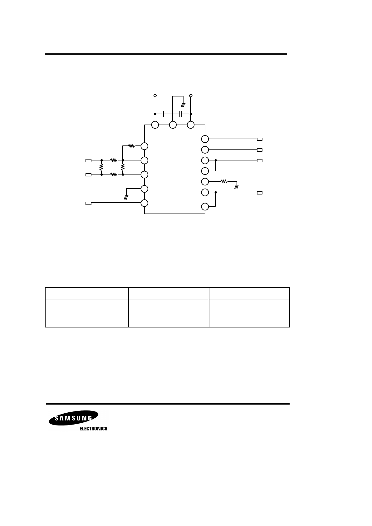
APPLICATION CIRCUIT
Fig. 4
NOTE 1 : Supposing Desired Line Termination Impedance RL = 600ohm
It is 0dBm = 0.77459Vrms
NOTE 2 : TX Gain 20 log (R2/R1), R1 + R2 < 100Kohm, or The Correspondence of 1-CHIP CODEC 0dBm 0 = 4dBm.
SELECTION OF MASTER CLOCK FREQUENCY
KT8554B/7B
µ
µ
BCLKR/CLKSEL KT 8554 KT 8557
Clocked
0
1 (or open)
1.536 / 1.544 MHz
2.048 MHz
1.536 / 1.544 MHz
2.048MHz
1.536 / 1.544 MHz
2.048MHz
 Loading...