

KS8993M/ML/MI
Integrated 3-Port 10/100 Managed
Switch with PHYs
Rev 1.04
General Description
The KS8993M, a highly integrated Layer 2 managed
switch, is designed for low port count, cost-sensitive
10/100 Mbps switch systems. It offers an extensive
feature set that includes tag/port-based VLAN,
quality of service (QoS) priority, management,
management information base (MIB) counters,
MII/SNI, and CPU control/data interfaces to
effectively address both current and emerging Fast
Ethernet applications.
The KS8993M contains two 10/100 transceivers with
patented mixed-signal low-power technology, three
media access control (MAC) units, a high-speed
non-blocking switch fabric, a dedicated address
lookup engine, and an on-chip frame buffer memory.
Both PHY units support 10BASE-T and 100BASETX. In addition, one of the PHY unit supports
100BASE-FX.
The KS8993ML is the single supply version with all
the identical rich features of the KS8993M.
___________________________________________________________________________________________________
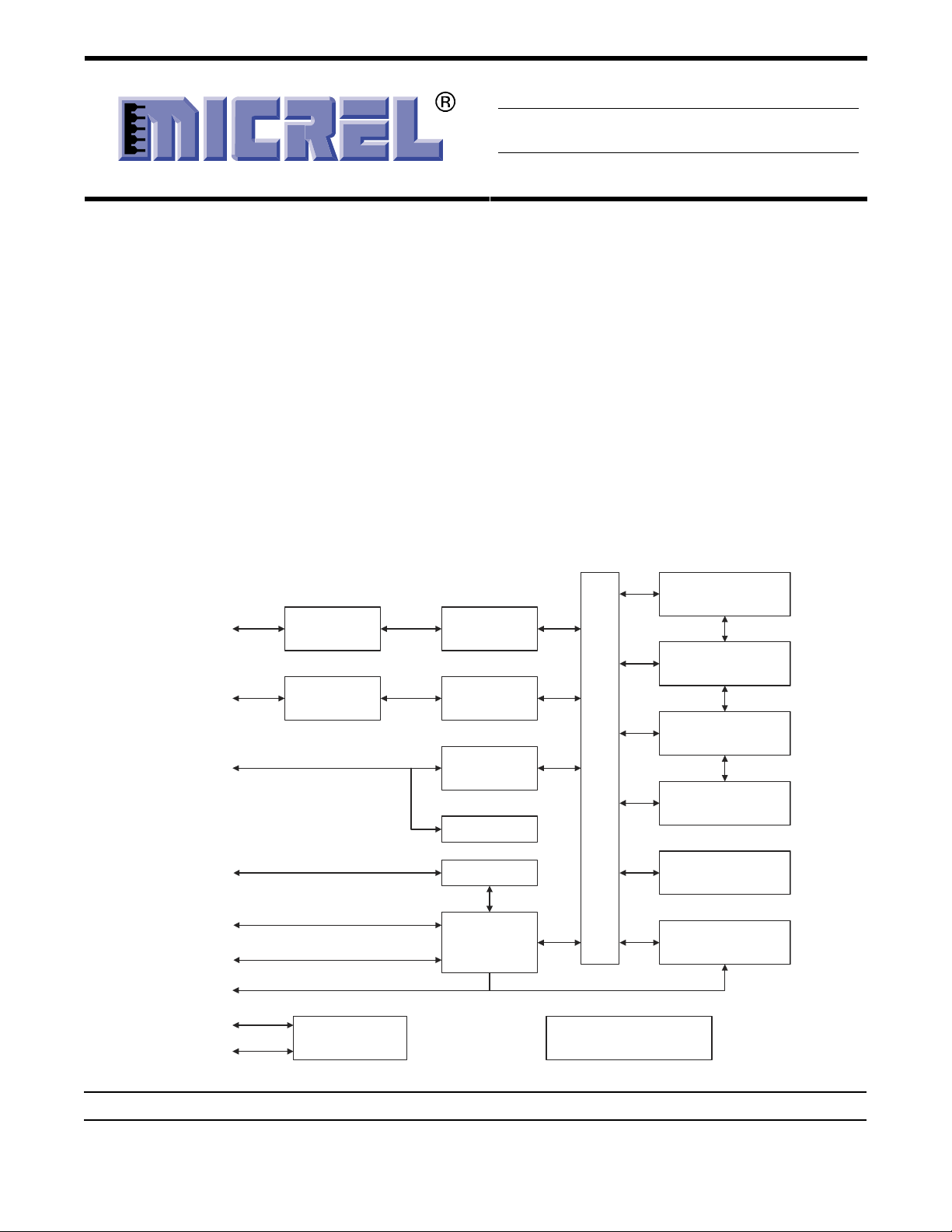
Functional Diagram
1KLook-Up
Engine
AUTO
MDI/MDI-X
AUTO
MDI/MDI-X
MII/SNI
10/100
T/TX/FX
PHY 1
10/100
T/TX
PHY 2
10/100
MAC1
10/100
MAC2
10/100
MAC3
SNI
FIFO,Flow Con trol
, VLANTagging,Priorit y
Queue
Management
Buffer
Management
Frame
Buffers
SPI
MIIM
SMI
I2C
P1 LED[3:0]
P2 LED[3:0]
LED
Drivers
Micrel Inc. • 2180 Fortune Drive • San Jose, CA 95131 • USA • tel +1 (
April 2005
SPI
Con t ro l
Registers
1
MIB
Cou nt e rs
EEPROM
Interface
Strap-In
Configuration Pins
408
) 944-0800 • fax + 1 (408) 474-1000 • http://www.micrel.com
M9999-041205

Micrel, Inc. KS8993M/ML/MI
Features
• Proven Integrated 3-Port 10/100 Ethernet Switch
– 2nd generation switch with three MACs and two
PHYs fully compliant to IEEE 802.3u standard
– Non-blocking switch fabric assures fast packet
delivery by utilizing a 1K MAC address lookup table
and a store-and-forward architecture
– Full duplex IEEE 802.3x flow control (pause) with
force mode option
– Half-duplex back pressure flow control
– Automatic MDI/MDI-X crossover with disable and
enable option
– 100BASE-FX support on port 1
– MII interface supports both MAC mode and PHY
mode
– 7-wire serial network interface (SNI) support for
legacy MAC
– Comprehensive LED Indicator support for link,
activity, full/half duplex and 10/100 speed
• Comprehensive Configuration Register Access
– Serial management interface (SMI) to all internal
registers
– MII management (MIIM) interface to PHY registers
– SPI and I
– I/0 Pins strapping and EEPROM to program
selective registers in unmanaged switch mode
– Control registers configurable on the fly (portpriority, 802.1p/d/q, AN…)
• QoS/CoS Packet Prioritization Support
– Per port, 802.1p and DiffServ-based
– Re-mapping of 802.1p priority field per port basis
• Advanced Switch Features
– IEEE 802.1q VLAN support for up to 16 groups
(full-range of VLAN ID)
– VLAN ID tag/untag options, per port basis
– IEEE 802.1p/q tag insertion or removal on a per
port basis (egress)
– Programmable rate limiting from 0Mbps to
100Mbps at the ingress and egress port, rate options
for high and low priority per port basis
– Broadcast storm protection with % control (global
and per port basis)
– IEEE 802.1d spanning tree protocol support
– Upstream special tagging mode to inform the
processor which ingress port receives the packet
– IGMP v1/v2 snooping support for multicast packet
filtering
– Double-tagging support
2
C Interface to all internal registers
• Switch Management Features
– Port mirroring/monitoring/sniffing: ingress and/or
egress traffic to any port or MII
– MIB counters for fully compliant statistics
gathering, 34 MIB counters per port
– Loopback modes for remote diagnostic of failure
• Low Power Dissipation: <0.8 Watts (includes PHY
transmit drivers)
– Full-chip hardware power-down (register
configuration not saved)
– Per port based software power-save on PHY (idle
link detection, register configuration preserved)
– 0.18um CMOS technology
– Voltages: Core 1.8V
I/O and Transceiver 3.3V
Use K8993ML for 3.3V only operation
• Industrial Temperature Range: –40
o
C to +85oC
• Available in128-Pin PQFP
Applications
• Universal Solutions
– Broadband gateway / Firewall / VPN
– Integrated DSL or cable modem multi-port router
– Wireless LAN access point + gateway
– Residential and enterprise VoIP gateway/phone
– Set-top/game box
– Home networking expansion
– Standalone 10/100 switch
– FTTx customer premises equipment
– Fiber broadband gateway
• Upgradeable Solutions
– Unmanaged switch with future option to migrate to
a managed solution
– Single PHY alternative with future expansion
option for two ports
• Industrial Solutions
– Applications requiring port redundancy and port
monitoring
– Sensor devices in redundant ring topology
Note:
1. The cost and time of PCB re-spin.
(1)
April 2005
2 M9999-041205

Micrel, Inc. KS8993M/ML/MI
Ordering Information
Part Number Temperature Range Package
KS8993M 0oC to 70oC 128-Pin PQFP
KS8993ML 0oC to 70oC 128-Pin PQFP
KS8993MI –40oC to +85oC 128-Pin PQFP
KSZ8993M 0oC to 70oC
KSZ8993ML 0oC to 70oC
128-Pin PQFP, Lead-free
128-Pin PQFP, Lead-free
April 2005
3 M9999-041205

Micrel, Inc. KS8993M/ML/MI
Revision History
Revision Date Summary of Changes
1.00 5/14/03 Created.
1.01 5/28/03 Added KS8993MI availability in Q4 2003.
1.02 12/8/03
1.03 9/22/04
1.04 4/12/05
Changed V
DDIO
, V
DDATX
and V
supply voltages
DDARX
from 3.3V to (3.3V or 2.5V).
Changed [PS1,PS0] = [1,1] setting from Reserved to SMI mode.
Changed Special Tagging Mode to Upstream Special Tagging Mode
(Switch port 3 to processor support only).
Updated recommended magnetic manufacturer list.
Added 25MHz crystal/oscillator clock’s ppm spec. in Pin Description.
Updated I
2
C Slave Serial Bus Configuration section.
Updated KS8993MI availability to from Q1 2004.
Added KS8993ML to General Description (page 1) and to the Functional
Description.
Updated Part Ordering Information table.
Updated pin description for pin 22 to the following:
V
core V
V
: For KS8993M, this is an input power pin for the 1.8V digital
DDC
.
DD
_1V8: For KS8993ML, this is an 1.8V output power pin to
OUT
supply the KS8993ML’s input power pins: V
(pin 63), V
(pins 91, 123), and V
DDC
DDA
DDAP
(pins 38,
43, 57).
Updated pin description for P1LED3 (pin 25) to indicate that an external
1K pull-down is needed if a LED is connected.
Updated pin description for MDIO (pin 95) to indicate that an external
4.7K pull-up is needed if this pin is in used.
Changed the aging period from 300 +/–75 seconds to about 200 seconds .
Updated Electrical Characteristics (V
, VIL, VOH, VOL).
IH
Transferred to new format.
Removed references to 2.5V operation
Added reset circuit recommendation
April 2005
4 M9999-041205

Micrel, Inc. KS8993M/ML/MI
Contents
List of Figures.........................................................................................................................................8
List of Tables...........................................................................................................................................8
Pin Description and I/O Assignment.....................................................................................................9
Pin Configuration ..................................................................................................................................19
Functional Description.........................................................................................................................20
Functional Overview: Physical Layer Transceiver............................................................................20
100BASE-TX Transmit.........................................................................................................................................................20
100BASE-TX Receive..........................................................................................................................................................20
PLL Clock Synthesizer........................................................................................................................................................21
Scrambler/De-scrambler (100BASE-TX Only)...................................................................................................................21
100BASE-FX Operation.......................................................................................................................................................21
100BASE-FX Signal Detection............................................................................................................................................21
100BASE-FX Far End Fault.................................................................................................................................................21
10BASE-T Transmit.............................................................................................................................................................21
10BASE-T Receive ..............................................................................................................................................................22
Power Management.............................................................................................................................................................22
MDI /MDI-X Auto Crossover................................................................................................................................................22
Straight Cable ................................................................................................................................................................23
Crossover Cable............................................................................................................................................................24
Auto Negotiation .................................................................................................................................................................24
Functional Overview: MAC and Switch ..............................................................................................26
Address Lookup..................................................................................................................................................................26
Learning...............................................................................................................................................................................26
Migration..............................................................................................................................................................................26
Aging....................................................................................................................................................................................26
Forwarding...........................................................................................................................................................................26
Switching Engine ................................................................................................................................................................29
MAC Operation....................................................................................................................................................................29
Inter Packet Gap (IPG)..................................................................................................................................................29
Back-Off Algorithm.........................................................................................................................................................29
Late Collision.................................................................................................................................................................29
Illegal Frames................................................................................................................................................................29
Flow Control...................................................................................................................................................................29
Half-Duplex Backpressure.............................................................................................................................................29
Broadcast Storm Protection...........................................................................................................................................30
MII Interface Operation........................................................................................................................................................30
SNI (7-Wire) Operation........................................................................................................................................................31
MII Management Interface (MIIM) .......................................................................................................................................31
Serial Management Interface (SMI)....................................................................................................................................32
Advanced Switch Functions................................................................................................................33
Spanning Tree Support.......................................................................................................................................................33
Upstream Special Tagging Mode.......................................................................................................................................34
IGMP Support ......................................................................................................................................................................35
“IGMP” Snooping...........................................................................................................................................................35
“Multicast Address Insertion” in the Static MAC Table...................................................................................................35
Port Mirroring Support........................................................................................................................................................35
IEEE 802.1Q VLAN Support................................................................................................................................................35
QoS Priority Support...........................................................................................................................................................36
Rate Limiting Support.........................................................................................................................................................38
Configuration Interface.......................................................................................................................................................38
I2C Master Serial Bus Configuration ..............................................................................................................................38
I2C Slave Serial Bus Configuration ................................................................................................................................39
SPI Slave Serial Bus Configuration ...............................................................................................................................39
Loopback Support...............................................................................................................................................................43
MII Management (MIIM) Registers.......................................................................................................44
Register 0: MII Basic Control..........................................................................................................................................45
April 2005
5 M9999-041205

Micrel, Inc. KS8993M/ML/MI
Register 1: MII Basic Status...........................................................................................................................................45
Register 2: PHYID HIGH................................................................................................................................................45
Register 3: PHYID LOW.................................................................................................................................................45
Register 4: Auto-Negotiation Advertisement Ability........................................................................................................46
Register 5: Auto-Negotiation Link Partner Ability ...........................................................................................................46
Register Map: Switch & PHY (8 bit registers).....................................................................................47
Global Registers.............................................................................................................................................................47
Port Registers ................................................................................................................................................................47
Advanced Control Registers...........................................................................................................................................47
Global Registers.................................................................................................................................................................. 47
Register 0 (0x00): Chip ID0............................................................................................................................................ 47
Register 1 (0x01): Chip ID1 / Start Switch......................................................................................................................48
Register 2 (0x02): Global Control 0................................................................................................................................48
Register 3 (0x03): Global Control 1................................................................................................................................49
Register 4 (0x04): Global Control 2................................................................................................................................49
Register 5 (0x05): Global Control 3................................................................................................................................50
Register 6 (0x06): Global Control 4................................................................................................................................51
Register 7 (0x07): Global Control 5................................................................................................................................52
Register 8 (0x08): Global Control 6................................................................................................................................52
Register 9 (0x09): Global Control 7................................................................................................................................52
Register 10 (0x0A): Global Control 8..............................................................................................................................52
Register 11 (0x0B): Global Control 9..............................................................................................................................52
Register 12 (0x0C): Reserved Register..........................................................................................................................53
Register 13 (0x0D): User Defined Register 1.................................................................................................................53
Register 14 (0x0E): User Defined Register 2 .................................................................................................................53
Register 15 (0x0F): User Defined Register 3 .................................................................................................................53
Port Registers......................................................................................................................................................................54
Register 16 (0x10): Port 1 Control 0...............................................................................................................................54
Register 32 (0x20): Port 2 Control 0...............................................................................................................................54
Register 48 (0x30): Port 3 Control 0...............................................................................................................................54
Register 17 (0x11): Port 1 Control 1...............................................................................................................................55
Register 33 (0x21): Port 2 Control 1...............................................................................................................................55
Register 49 (0x31): Port 3 Control 1...............................................................................................................................55
Register 18 (0x12): Port 1 Control 2...............................................................................................................................56
Register 34 (0x22): Port 2 Control 2...............................................................................................................................56
Register 50 (0x32): Port 3 Control 2...............................................................................................................................56
Register 19 (0x13): Port 1 Control 3...............................................................................................................................56
Register 35 (0x23): Port 2 Control 3...............................................................................................................................56
Register 51 (0x33): Port 3 Control 3...............................................................................................................................56
Register 20 (0x14): Port 1 Control 4...............................................................................................................................57
Register 36 (0x24): Port 2 Control 4...............................................................................................................................57
Register 52 (0x34): Port 3 Control 4...............................................................................................................................57
Register 21 (0x15): Port 1 Control 5...............................................................................................................................57
Register 37 (0x25): Port 2 Control 5...............................................................................................................................57
Register 53 (0x35): Port 3 Control 5...............................................................................................................................57
Register 22 (0x16): Port 1 Control 6...............................................................................................................................57
Register 38 (0x26): Port 2 Control 6...............................................................................................................................57
Register 54 (0x36): Port 3 Control 6...............................................................................................................................57
Register 23 (0x17): Port 1 Control 7...............................................................................................................................57
Register 39 (0x27): Port 2 Control 7...............................................................................................................................57
Register 55 (0x37): Port 3 Control 7...............................................................................................................................57
Register 24 (0x18): Port 1 Control 8...............................................................................................................................57
Register 40 (0x28): Port 2 Control 8...............................................................................................................................57
Register 56 (0x38): Port 3 Control 8...............................................................................................................................57
Register 25 (0x19): Port 1 Control 9...............................................................................................................................58
Register 41 (0x29): Port 2 Control 9...............................................................................................................................58
Register 57 (0x39): Port 3 Control 9...............................................................................................................................58
Register 26 (0x1A): Port 1 Control 10 ............................................................................................................................58
Register 42 (0x2A): Port 2 Control 10 ............................................................................................................................58
Register 58 (0x3A): Port 3 Control 10 ............................................................................................................................58
Register 27 (0x1B): Port 1 Control 11 ............................................................................................................................58
Register 43 (0x2B): Port 2 Control 11 ............................................................................................................................58
April 2005
6 M9999-041205

Micrel, Inc. KS8993M/ML/MI
Register 59 (0x3B): Port 3 Control 11 ............................................................................................................................58
Register 28 (0x1C): Port 1 Control 12............................................................................................................................59
Register 44 (0x2C): Port 2 Control 12............................................................................................................................59
Register 60 (0x3C): Reserved, not applied to port 3 ......................................................................................................59
Register 29 (0x1D): Port 1 Control 13............................................................................................................................60
Register 45 (0x2D): Port 2 Control 13............................................................................................................................60
Register 61 (0x3D): Reserved, not applied to port 3 ......................................................................................................60
Register 30 (0x1E): Port 1 Status 0................................................................................................................................61
Register 46 (0x2E): Port 2 Status 0................................................................................................................................61
Register 62 (0x3E): Reserved, not applied to port 3 ......................................................................................................61
Register 31 (0x1F): Port 1 Status 1................................................................................................................................62
Register 47 (0x2F): Port 2 Status 1................................................................................................................................62
Register 63 (0x3F): Port 3 Status 1................................................................................................................................62
Advanced Control Registers..............................................................................................................................................63
Register 96 (0x60): TOS Priority Control Register 0.......................................................................................................63
Register 97 (0x61): TOS Priority Control Register 1.......................................................................................................63
Register 98 (0x62): TOS Priority Control Register 2.......................................................................................................63
Register 99 (0x63): TOS Priority Control Register 3.......................................................................................................63
Register 100 (0x64): TOS Priority Control Register 4.....................................................................................................63
Register 101 (0x65): TOS Priority Control Register 5.....................................................................................................63
Register 102 (0x66): TOS Priority Control Register 6.....................................................................................................63
Register 103 (0x67): TOS Priority Control Register 7.....................................................................................................63
Register 104 (0x68): MAC Address Register 0 ..............................................................................................................64
Register 105 (0x69): MAC Address Register 1 ..............................................................................................................64
Register 106 (0x6A): MAC Address Register 2..............................................................................................................64
Register 107 (0x6B): MAC Address Register 3..............................................................................................................64
Register 108 (0x6C): MAC Address Register 4..............................................................................................................64
Register 109 (0X6D): MAC Address Register 5 .............................................................................................................64
Register 110 (0x6E): Indirect Access Control 0..............................................................................................................65
Register 111 (0x6F): Indirect Access Control 1..............................................................................................................65
Register 112 (0x70): Indirect Data Register 8................................................................................................................65
Register 113 (0x71): Indirect Data Register 7................................................................................................................65
Register 114 (0x72): Indirect Data Register 6................................................................................................................65
Register 115 (0x73): Indirect Data Register 5................................................................................................................65
Register 116 (0x74): Indirect Data Register 4................................................................................................................65
Register 117 (0x75): Indirect Data Register 3................................................................................................................66
Register 118 (0x76): Indirect Data Register 2................................................................................................................66
Register 119 (0x77): Indirect Data Register 1................................................................................................................66
Register 120 (0x78): Indirect Data Register 0 ................................................................................................................66
Registers 121 to 127......................................................................................................................................................66
Static MAC Address Table.............................................................................................................................................66
VLAN Table.................................................................................................................................................................... 67
Dynamic MAC Address Table ........................................................................................................................................68
MIB (Management Information Base) Counters.............................................................................................................69
Additional Information.....................................................................................................................................................72
Absolute Maximum Ratings .................................................................................................................73
Operating Ratings.................................................................................................................................73
Electrical Characteristics.....................................................................................................................74
Timing Specifications...........................................................................................................................76
EEPROM Timing..................................................................................................................................................................76
SNI Timing............................................................................................................................................................................77
MII Timing….……………………………………………………………………………………………………………………………77
MAC Mode MII Timing....................................................................................................................................................78
PHY-Mode MII Timing....................................................................................................................................................79
SPI Timing….…………………………………………………………………………………………………………………………...77
Input Timing ...................................................................................................................................................................80
Output Timing.................................................................................................................................................................81
Reset Timing........................................................................................................................................................................82
Selection of Isolation Transformers....................................................................................................84
Selection of Reference Crystal............................................................................................................84
Package Information.............................................................................................................................85
April 2005
7 M9999-041205

Micrel, Inc. KS8993M/ML/MI
List of Figures
Figure 1. Typical Straight Cable Connection .......................................................................................................................................24
Figure 2. Typical Crossover Cable Connection...................................................................................................................................24
Figure 3. Auto Negotiation and Parallel Operation .............................................................................................................................25
Figure 4. Destination Address Lookup Flow Chart, Stage 1..............................................................................................................27
Figure 5. Destination Address Resolution Flow Chart, Stage 2 ........................................................................................................28
Figure 6. 802.1p Priority Field Format ..................................................................................................................................................37
Figure 7. KS8993M EEPROM Configuration Timing Diagram............................................................................................................38
Figure 8. SPI Write Data Cycle...............................................................................................................................................................41
Figure 9. SPI Read Data Cycle...............................................................................................................................................................41
Figure 10. SPI Multiple Write..................................................................................................................................................................41
Figure 11. SPI Multiple Read..................................................................................................................................................................42
Figure 12. Loopback Path ......................................................................................................................................................................43
Figure 13. EEPROM Interface Input Timing Diagram..........................................................................................................................76
Figure 14. EEPROM Interface Output Timing Diagram.......................................................................................................................76
Figure 15. SNI Input Timing Diagram....................................................................................................................................................77
Figure 16. SNI Output Timing Diagram.................................................................................................................................................77
Figure 17. MAC-Mode MII Timing – Data Received from MII ..............................................................................................................78
Figure 18. MAC-Mode MII Timing – Data Input to MII ..........................................................................................................................78
Figure 19. PHY-Mode MII Timing – Data Received from MII ...............................................................................................................79
Figure 20. PHY-Mode MII Timing – Data Input to MII...........................................................................................................................79
Figure 21. SPI Input Timing....................................................................................................................................................................80
Figure 22. SPI Output Timing.................................................................................................................................................................81
Figure 23. Reset Timing .........................................................................................................................................................................82
128-Pin PQFP Package...........................................................................................................................................................................85
List of Tables
Table 1. FX and TX Mode Selection ......................................................................................................................................................21
Table 2. MDI/MDI-X Pin Definitions........................................................................................................................................................22
Table 3. MII Signals.................................................................................................................................................................................30
Table 4. SNI Signals................................................................................................................................................................................31
Table 5. MII Management Interface Frame Format ..............................................................................................................................32
Table 6. Serial Management Interface (SMI) Frame Format................................................................................................................32
Table 7. Upstream Special Tagging Mode Format ..............................................................................................................................34
Table 8. STPID Egress Rules (Switch Port 3 to Processor)................................................................................................................34
Table 9. FID+DA Lookup in VLAN Mode...............................................................................................................................................36
Table 10. FID+SA Lookup in VLAN Mode.............................................................................................................................................36
Table 11. KS8993M SPI Connections....................................................................................................................................................40
Table 12. Format of Static MAC Table (8 Entries)................................................................................................................................66
Table 13. Format of Static VLAN Table (16 Entries)............................................................................................................................68
Table 14. Format of Dynamic MAC Address Table (1K Entries)........................................................................................................68
Table 15. Format of “Per Port” MIB Counters......................................................................................................................................69
Table 16. Port 1s “Per Port” MIB Counters Indirect Memory Offsets................................................................................................70
Table 17. Port 1’s “Per Port” MIB Counters Indirect Memory Offsets...............................................................................................71
Table 18. Format of “All Port Dropped Packet” MIB Counters ..........................................................................................................71
Table 19. “All Port Dropped Packet” MIB Counters Indirect Memory Offsets .................................................................................71
Table 20. EEPROM Timing Parameters ................................................................................................................................................76
Table 21. SNI Timing Parameters ..........................................................................................................................................................77
Table 22. MAC-Mode MII Timing Parameters .......................................................................................................................................78
Table 23. PHY-Mode MII Timing Parameters........................................................................................................................................79
Table 24. SPI Input Timing Parameters ................................................................................................................................................80
Table 25. SPI Output Timing Parameters .............................................................................................................................................81
Table 26. Reset Timing Parameters ......................................................................................................................................................82
Table 27. Transformer Selection Criteria..............................................................................................................................................84
Table 28. Qualified Single Port Magnetics ...........................................................................................................................................84
Table 29. Typical Reference Crystal Characteristics ..........................................................................................................................84
April 2005
8 M9999-041205
Micrel, Inc. KS8993M/ML/MI
Pin Description and I/O Assignment
Pin Number Pin Name Type
1
2
3
4
5
6
7 DGND Gnd Digital ground
Note:
1. Ipu/O = Input with internal pull-up during reset, output pin otherwise.
Gnd = Ground.
P1LED2
P1LED1
P1LED0
P2LED2
P2LED1
P2LED0
(1)
Description
Ipu/O
Ipu/O
Ipu/O
Ipu/O
Ipu/O
Ipu/O
Port 1 LED indicators
[LEDSEL1, LEDSEL0]
[0, 0] [0, 1]
P1LED3 — —
P1LED2 Link/Act 100Link/Act
P1LED1 Full duplex/Col 10Link/Act
P1LED0 Speed Full duplex
[LEDSEL1, LEDSEL0]
[1, 0] [1, 1]
P1LED3 Act —
P1LED2 Link —
P1LED1 Full duplex/Col —
P1LED0 Speed —
Notes:
LEDSEL0 is external strap-in pin 70.
LEDSEL1 is external strap-in pin 23.
P1LED3 is pin 25.
During reset, P1LED[2:0] are inputs for internal testing.
Port 2 LED indicators
[LEDSEL1, LEDSEL0]
[0, 0] [0, 1]
P2LED3 — —
P2LED2 Link/Act 100Link/Act
P2LED1 Full duplex/Col 10Link/Act
P2LED0 Speed Full duplex
[LEDSEL1, LEDSEL0]
[1, 0] [1, 1]
P2LED3 Act —
P2LED2 Link —
P2LED1 Full duplex/Col —
P2LED0 Speed —
Notes:
LEDSEL0 is external strap-in pin 70.
LEDSEL1 is external strap-in pin 23.
P2LED3 is pin 20.
During reset, P2LED[2:0] are inputs for internal testing.
April 2005
9 M9999-041205

Micrel, Inc. KS8993M/ML/MI
Pin Number Pin Name Type
8 VDDIO P 3.3V dig ital VDD
9 NC Ipd No connect
10 NC Ipd No connect
11 NC Ipu No connect
12 ADVFC Ipu
13 P2ANEN Ipu 1 = enable auto negotiation on port 2
14 P2SPD Ipd 1 = force port 2 to 100BT if P2ANEN = 0
15 P2DPX Ipd
16 P2FFC Ipd 1 = always enable (force) port 2 flow control feature
17 NC Opu No connect
18 NC Ipd No connect
19 NC Ipd No connect
20 P2LED3 Opd Port 2 LED indicator
21 DGND Gnd Digital ground
22
VDDC/VOUT_1
V8
23 LEDSEL1 Ipd LED display mode select
24 NC O No connect
25 P1LED3 Opd Port 1 LED indicator
(1)
Description
1 = advertise the switch’s flow control capability via auto
negotiation.
0 = will not advertise the switch’s flow control capability via
auto negotiation.
0 = disable auto negotiation on port 2
0 = force port 2 to 10BT if P2ANEN = 0
1 = port 2 default to full duplex mode if P2ANEN = 1 and auto
negotiation fails. Force port 2 in full duplex mode if P2ANEN
= 0.
0 = port 2 default to half duplex mode if P2ANEN = 1 and
auto negotiation fails. Force port 2 in half duplex mode if
P2ANEN = 0.
0 = port 2 flow control feature enable is determined by auto
negotiation result.
Note: Internal pull-down is weak; it will not turn ON the LED.
See description in pin 4.
V
P
: For KS8993M, this is an input power pin for the 1.8V
DDC
digital core V
V
OUT_1V8
supply the KS8993ML’s input power pins: V
(pins 91 and 123), and V
V
DDC
See description in pins 1 and 4.
Note: An external 1K pull-down is needed on this pin if it is
connected to a LED. The 1K resistor will not turn ON the
LED.
See description in pin 1.
.
DD
: For KS8993ML, this is a 1.8V output power pin to
(pin 63),
(pins 38, 43, and 57).
DDA
DDAP
Note:
1. P = Power supply.
Gnd = Ground.
O = Output.
Ipu = Input w/ internal pull-up.
Ipd = Input w/ internal pull-down.
Opu = Output with internal pull-up. Opd = Output internal pull-down.
April 2005
10 M9999-041205

Micrel, Inc. KS8993M/ML/MI
Pin Number Pin Name Type
26 NC O No connect
27 HWPOVR Ipd Hardware pin overwrite
28 P2MDIXDIS Ipd Port 2 Auto MDI/MDI-X
29 P2MDIX Ipd Port 2 MDI/MDI-X setting when auto MDI/MDI-X is disabled.
30 P1ANEN Ipu 1 = enable auto negotiation o n port 1
31 P1SPD Ipd 1 = force port 1 to 100BT if P1ANEN = 0
32 P1DPX Ipd
33 P1FFC Ipd 1 = always enable (force) port 1 flow control feature
34 NC Ipd No connect
35 NC Ipd No connect
36 PWRDN Ipu Chip power-down input (active low)
37 AGND Gnd Analog ground
38 VDDA P 1.8V analog VDD
39 AGND Gnd Analog ground
40 MUX1 I Factory test pin - float for normal operation
41 MUX2 I Factory test pin - float for normal operation
42 AGND Gnd Analog ground
43 VDDA P 1.8V analog VDD
44 FXSD1 I Fiber signal detect/factory test pin
(1)
Description
0 = Disable. All strap-in pins configurations are overwritten by
the EEPROM configuration data
1 = Enable. All strap-in pins configurations are overwritten by
the EEPROM configuration data, except for register 0x2C bits
[7:5], (port 2: auto-negotiation enable, force speed, force
duplex).
PD (default) = enable
PU = disable
PD (default) = MDI-X (transmit on TXP2 / TXM2 pins)
PU = MDI, (transmit on RXP2 / RXM2 pins)
0 = disable auto negotiation on port 1
0 = force port 1 to 10BT if P1ANEN = 0
1 = port 1 default to full duplex mode if P1ANEN = 1 and auto
negotiation fails. Force port 1 in full-duplex mode if P1ANEN
= 0.
0 = port 1 default to half duplex mode if P1ANEN = 1 and auto
negotiation fails. Force port 1 in half duplex mode if P1ANEN
= 0.
0 = port 1 flow control feature enable is determined by auto
negotiation result.
Note:
1. P = Power supply.
Gnd = Ground.
I = Input.
O = Output.
Ipu = Input w/ internal pull-up.
Ipd = Input w/ internal pull-down.
April 2005
11 M9999-041205

Micrel, Inc. KS8993M/ML/MI
Pin Number Pin Name Type
45 RXP1 I/O Physical receive or transmit signal (+ differential)
46 RXM1 I/O Physical receive or transmit signal (– differential)
47 AGND Gnd Analog ground
48 TXP1 I/O Physical transmit or receive signa l (+ differential)
49 TXM1 I/O Physical transmit or receive signal (– differential)
50 VDDATX P 3.3V analog VDD
51 VDDARX P 3.3V analog VDD
52 RXM2 I/O Physical receive or transmit signal (– differential)
53 RXP2 I/O Physical receive or transmit signal (+ differential)
54 AGND Gnd Analog ground.
55 TXM2 I/O Physical transmit or receive signal (– differential)
56 TXP2 I/O Physical transmit or receive signa l (+ differential)
57 VDDA P 1.8 analog VDD
58 AGND Gnd Analog ground
59 TEST1 I Factory test pin - float for normal operation
60 TEST2 Ipu Factory test pin - float or pull-up for normal operation
61 ISET O Set physical transmit output current.
62 AGND Gnd Analog ground
63 VDDAP P 1.8V analog VDD for PLL
64 AGND Gnd Analog ground.
65
66
X1
X2
67 RST_N Ipu Hardware reset pin (active low)
68 BPEN Ipd Half-duplex backpressure
69 SMAC Ipd Special Mac-mode
(1)
Description
Pull-down this pin with a 3.01K 1% resistor to ground.
I
O
25MHz crystal/oscillator clock connections
Pins (X1, X2) connect to a crystal. If an oscillator is used, X1
connects to a 3.3V tolerant oscillator and X2 is a no connect.
Note: Clock is +/- 50ppm for both crystal and oscillator.
1 = enable
0 = disable
In this mode, the switch will do faster back-offs than normal.
1 = enable
0 = disable
Note:
1. P = Power supply.
Gnd = Ground.
I = Input.
O = Output.
Ipu = Input w/ internal pull-up.
Ipd = Input w/ internal pull-down.
April 2005
12 M9999-041205

Micrel, Inc. KS8993M/ML/MI
Pin Number Pin Name Type
(1)
Description
70 LEDSEL0 Ipd LED display mode select
See description in pins 1 and 4.
71 SMTXEN Ipd Switch MII transmit enable
72 SMTXD3 Ipd Switch MII transmit data bit 3
73 SMTXD2 Ipd Switch MII transmit data bit 2
74 SMTXD1 Ipd Switch MII transmit data bit 1
75 SMTXD0 Ipd Switch MII transmit data bit 0
76 SMTXER Ipd Switch MII transmit error
77 SMTXC Ipd/O Switch MII transmit clock
Output in PHY MII mode
Input in MAC MII mode
78 DGND Gnd Digital ground
79 VDDIO P 3.3V digital VDD
80 SMRXC Ipd/O Switch MII receive clock.
Output in PHY MII mode
Input in MAC MII mode
81 SMRXDV O Switch MII receive data valid
82 SMRXD3 Ipd/O Switch MII receive data bit 3
Strap option: switch MII full-duplex flow control
PD (default) = disable
PU = enable
83 SMRXD2 Ipd/O Switch MII receive bit 2
Strap option: switch MII is in
PD (default) = full-duplex mode
PU = half-duplex mode
84 SMRXD1 Ipd/O Switch MII receive bit 1
Strap option: Switch MII is in
PD (default) = 100Mbps mode
PU = 10Mbps mode
85 SMRXD0 Ipd/O Switch MII receive bit 0
Strap option: switch will accept packet size up to
PD (default) = 1536 bytes (inclusive)
PU = 1522 bytes (tagged), 1518 bytes (untagged)
86 SCOL Ipd/O Switch MII collision detect
87 SCRS Ipd/O Switch MII carrier sense
Note:
1. P = Power supply.
Gnd = Ground.
O = Output.
Ipd = Input w/ internal pull-down.
Ipd/O = Input w/ internal pull-down during reset, output pin otherwise.
April 2005
13 M9999-041205

Micrel, Inc. KS8993M/ML/MI
Pin Number Pin Name Type
88
89
SCONF1
SCONF0
(1)
Description
Ipd
Ipd
Switch MII interface configuration
(SCONF1, SCONF0) Description
(0,0) disable, outputs tri-stated
(0,1) PHY mode MII
(1,0) MAC mode MII
(1,1) PHY mode SNI
90 DGND Gnd Digital ground
91 VDDC P 1.8V digital VDD
92
93
PRSEL1
PRSEL0
Ipd
Ipd
Priority select. Select queue servicing if using split queues.
Use the table below to select the desired servicing. Note that
this selection effects all split transmit queue ports in the same
way.
(PRSEL1, PRSEL0) Description
(0,0)
(0,1)
(1,0)
(1,1)
Transmit all high priority before low
priority
Transmit high priority and low priority at
10:1 ratio.
Transmit high priority and low priority at
5:1 ratio.
Transmit high priority and low priority at
2:1 ratio.
94 MDC Ipu MII management interface: clock input
95 MDIO Ipu/O MII management interface: data input/output
Note: an external 4.7K pull-up is needed on this pin when it is
in use.
96 SPIQ Opu SPI slave mode: serial data output
See description in pins 100 and 101.
97 SCL Ipu/O
SPI slave mode / I2C slave mode: clock input
I2C master mode: clock output
See description in pins 100 and 101.
98 SDA Ipu/O SPI slave mode: serial data input
2
I
C master/slave mode: serial data input/output
See description in pins 100 and 101.
99 SPIS_N Ipu SPI slave mode: chip select (active low)
When SPIS_N is high, the KS8993M is deselected and SPIQ
is held in high impedance state.
A high-to-low transition is used to initiate SPI data transfer.
See description in pins 100 and 101.
Note:
1. P = Power supply.
Gnd = Ground.
Ipu = Input w/ internal pull-up.
Ipd = Input w/ internal pull-down.
Ipu/O = Input w/ internal pull-up during reset, output pin otherwise.
Opu = Output w/ internal pull-up.
April 2005
14 M9999-041205
Micrel, Inc. KS8993M/ML/MI
Pin Number Pin Name Type
100
101
PS1
PS0
(1)
Description
Ipd
Ipd
Serial bus configuration pins to select mode of access to
KS8993M internal registers.
[PS1, PS0] = [0, 0] — I
(If EEPROM is not detected, the power-up default values of
the KS8993M internal registers will be used.)
Interface Signals Type Description
SPIQ O Not used (tri-stated)
SCL O I2C clock
SDA I/O I2C data I/O
SPIS_N Ipu Not used
[PS1, PS0] = [0, 1] — I2C slave mode
The external I2C master will drive the SCL clock.
The KS8993M device addresses are:
1011_1111 <read>
1011_1110 <write>
Interface Signals Type Description
SPIQ O Not used (tri-stated)
SCL I I2C clock
SDA I/O I2C data I/O
SPIS_N Ipu Not used
2
C master (EEPROM) mode
[PS1, PS0] = [1, 0] — SPI slave mode
Interface Signals Type Description
SPIQ O SPI data out
SCL I SPI clock
SDA I SPI data In
SPIS_N Ipu SPI chip select
[PS1, PS0] = [1, 1] – SMI-mode
In this mode, the KS8993M provides access to all its internal
8 bit registers through its MDC and MDIO pins.
Note:
When (PS1, PS0) ≠ (1,1), the KS8993M provides access to
its 16 bit MIIM registers through its MDC and MDIO pins.
102
103
PV31
PV32
Ipu
Ipu
Port 3 port-based VLAN mask bits – Use to select which
ports may transmit packets received on port 3.
PV31 = 1, port 1 may transmit packets received on port 3
PV31 = 0, port 1 will not transmit any packets received on
port 3
PV32 = 1, port 2 may transmit packets received on port 3
PV32 = 0, port 2 will not transmit any packets received on
port 3
Note:
1. I = Input. Ipu = Input w/ internal pull-up. I/O = Bi-directional.
O= Output. Ipd = Input w/ internal pull-down.
April 2005
15 M9999-041205

Micrel, Inc. KS8993M/ML/MI
Pin Number Pin Name Type
104
105
PV21
PV23
(1)
Description
Ipu
Ipu
Port 2 port-based VLAN mask bits – Use to select which
ports may transmit packets received on port 2.
PV21 = 1, port 1 may transmit packets received on port 2
PV21 = 0, port 1 will not transmit any packets received on
port 2
PV23 = 1, port 3 may transmit packets received on port 2
PV23 = 0, port 3 will not transmit any packets received on
port 2
106 DGND Gnd Digital ground
107 VDDIO P
108
109
PV12
PV13
Ipu
Ipu
3.3V digital VDD
Port 1 port-based VLAN mask bits – Use to select which
ports may transmit packets received on port 1.
PV12 = 1, port 2 may transmit packets received on port 1
PV12 = 0, port 2 will not transmit any packets received on
port 1
PV13 = 1, port 3 may transmit packets received on port 1
PV13 = 0, port 3 will not transmit any packets received on
port 1
110 P3_1PEN Ipd
Enable 802.1p priority classification on port 3 ingress
1 = enable
0 = disable
Enable is from the receive perspective. If 802.1p processing
is disabled or there is no tag, priority is determined by the
P3_PP pin.
111 P2_1PEN Ipd
Enable 802.1p priority classification on port 2 ingress
1 = enable
0 = disable
Enable is from the receive perspective. If 802.1p processing
is disabled or there is no tag, priority is determined by the
P2_PP pin.
112 P1_1PEN Ipd
Enable 802.1p priority classification on port 1 ingress
1 = enable
0 = disable
Enable is from the receive perspective. If 802.1p processing
is disabled or there is no tag, priority is determined by the
P1_PP pin.
113 P3_TXQ2 Ipd
Select transmit queue split on port 3
1 = split
0 = no split
The split sets up high and low priority queues. Packet priority
classification is done on ingress ports, via port-based, 802.1p
or TOS based scheme. The priority enabled queuing on port 3
is set by P3_TXQ2.
Note:
1. P = Power supply.
Gnd = Ground.
Ipu = Input w/ internal pull-up. Ipd = Input w/ internal pull-down.
April 2005
16 M9999-041205

Micrel, Inc. KS8993M/ML/MI
Pin Number Pin Name Type
114 P2_TXQ2 Ipd
115 P1_TXQ2 Ipd
116 P3_PP Ipd
117 P2_PP Ipd
118 P1_PP Ipd
119 P3_TAGINS Ipd
120 P2_TAGINS Ipd
(1)
Description
Select transmit queue split on port 2
1 = split
0 = no split
The split sets up high and low priority queues. Packet priority
classification is done on ingress ports, via port-based, 802.1p
or TOS based scheme. The priority enabled queuing on port 2
is set by P2_TXQ2.
Select transmit queue split on port 1
1 = split
0 = no split
The split sets up high and low priority queues. Packet priority
classification is done on ingress ports, via port-based, 802.1p
or TOS based scheme. The priority enabled queuing on port 1
is set by P1_TXQ2.
Select port-based priority on port 3 ingress
1 = high
0 = low <default>
802.1p and DiffServ, if applicable, takes precedence.
Select port-based priority on port 2 ingress
1 = high
0 = low <default>
802.1p and DiffServ, if applicable, takes precedence.
Select port-based priority on port 1 ingress
1 = high
0 = low <default>
802.1p and DiffServ, if applicable, takes precedence.
Enable tag insertion on port 3 egress
1 = enable
0 = disable
All packets transmitted from port 3 will have 802.1Q tag.
Packets received with tag will be sent out intact. Packets
received without tag will be tagged with ingress port’s default
tag.
Enable tag insertion on port 2 egress
1 = enable
0 = disable
All packets transmitted from port 2 will have 802.1Q tag.
Packets received with tag will be sent out intact. Packets
received without tag will be tagged with ingress port’s default
tag.
Note:
1. Ipd = Input w/ internal pull-down.
April 2005
17 M9999-041205

Micrel, Inc. KS8993M/ML/MI
Pin Number Pin Name Type
121 P1_TAGINS Ipd
122 DGND Gnd Digital ground
123 VDDC P
124 P3_TAGRM Ipd
125 P2_TAGRM Ipd
126 P1_TAGRM Ipd
127 T E STEN Ipd Scan Test Enable
128 SCANEN Ipd Scan Test Scan Mux Enable
Note:
1. P = Power supply.
Gnd = Ground.
Ipd = Input w/ internal pull-down.
(1)
Description
Enable tag insertion on port 1 egress
1 = enable
0 = disable
All packets transmitted from port 1 will have 802.1Q tag.
Packets received with tag will be sent out intact. Packets
received without tag will be tagged with ingress port’s default
tag.
1.8V digital VDD
Enable tag removal on port 3 egress
1 = enable
0 = disable
All packets transmitted from port 3 will not have 802.1Q tag.
Packets received with tag will be modified by removing
802.1Q tag. Packets received without tag will be sent out
intact.
Enable tag removal on port 2 egress
1 = enable
0 = disable
All packets transmitted from port 2 will not have 802.1Q tag.
Packets received with tag will be modified by removing
802.1Q tag. Packets received without tag will be sent out
intact.
Enable tag removal on port 1 egress
1 = enable
0 = disable
All packets transmitted from port 1 will not have 802.1Q tag.
Packets received with tag will be modified by removing
802.1Q tag. Packets received without tag will be sent out
intact.
For normal operation, pull-down this pin to ground.
For normal operation, pull-down this pin to ground.
April 2005
18 M9999-041205
Micrel, Inc. KS8993M/ML/MI
S
Pin Configuration
PV32
PV21
PV23
DGND
VDDIO
PV12
PV13
P3_1PEN
P2_1PEN
P1_1PEN
P3_TXQ2
P2_TXQ2
P1_TXQ2
P3_PP
P2_PP
P1_PP
P3_TAGINS
P2_TAGINS
P1_TAGINS
DGND
VDDC
P3_TAGRM
P2_TAGRM
P1_TAGRM
TESTEN
SCANEN
PV31
PS0
PS1
SPIS_N
SDA
SCL
SPIQ
MDIO
MDC
PRSEL0
PRSEL1
VDDC
DGND
SCONF0
SCONF1
SCRS
SCOL
SMRXD0
SMRXD1
SMRXD2
SMRXD3
SMRXDV
SMRXC
VDDIO
DGND
SMTXC
SMTXER
SMTXD0
SMTXD1
SMTXD2
SMTXD3
SMTXEN
LEDSEL0
SMAC
BPEN
RST_NX2X1
AGND
VDDAP
AGND
ISET
TEST2
TEST1
AGND
VDDA
TXP2
TXM2
AGND
RXP2
RXM2
VDDARX
VDDATX
TXM1
TXP1
AGND
RXM1
RXP1
FXSD1
VDDA
AGND
MUX2
MUX1
AGND
P1LED2
P1LED1
P1LED0
P2LED2
P2LED1
P2LED0
DGND
VDDIO
NCNCNC
P2SPD
ADVFC
P2ANEN
NCNCNC
P3FFC
P2DPX
P2LED3
VDDC
DGND
NC
NC
P1LED3
LEDSEL1
P2MDIX
P1ANEN
HWPOVR
P2MDIXDI
P1FFC
P1SPD
P1DPX
NC
NC
PWRDN
VDDA
AGND
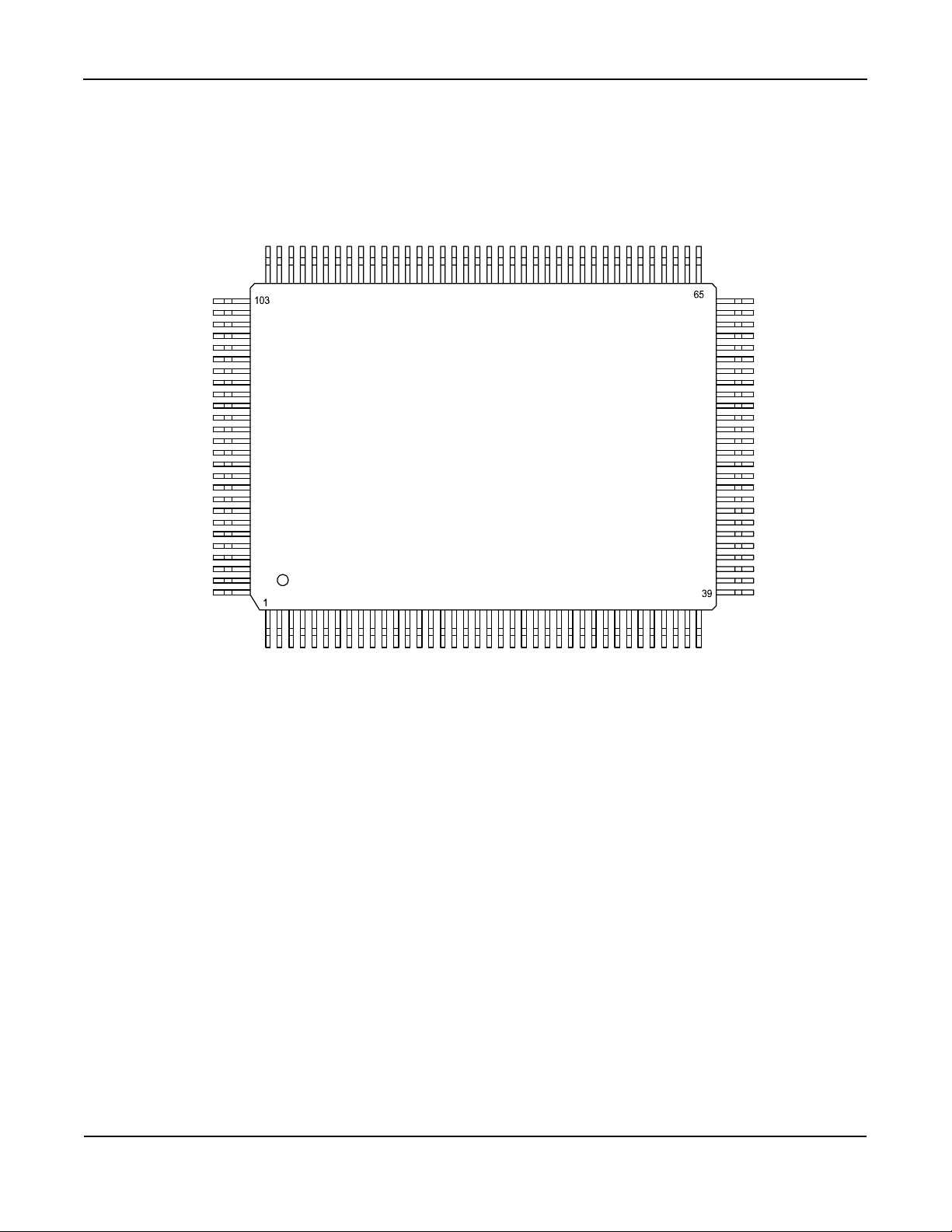
128-Pin PQFP (Top View)
April 2005
19 M9999-041205

Micrel, Inc. KS8993M/ML/MI
Functional Description
The KS8993M contains two 10/100 physical layer transceivers and three MAC units with an integrated Layer 2
managed switch.
The KS8993M has the flexibility to reside in either a managed or unmanaged design. In a managed design, the
host processor has complete control of the KS8993M via the SMI interface, MIIM interface, SPI bus, or I
2
C bus.
An unmanaged design is achieved through I/O strapping and/or EEPROM programming at system reset time.
On the media side, the KS8993M supports IEEE 802.3 10BASE-T and 100BASE-TX on both PHY ports, and
100BASE-FX on PHY port 1. The KS8993M can be used as a media converter.
The KS8993ML is the single supply version with all the identical rich features of the KS8993M. In the KS8993ML
version, pin number 22 provides 1.8V output power to the KS8993ML’s V
DDC
, V
DDA
, and V
power pins. Refer
DDAP
to the Pin Description table for information about pin 22 (Pin Description and I/0 Assignment).
Physical signal transmission and reception are enhanced through the use of patented analog circuitries that make
the design more efficient and allow for lower power consumption and smaller chip die size.
Functional Overview: Physical Layer Transceiver
100BASE-TX Transmit
The 100BASE-TX transmit function performs parallel to serial conversion, 4B/5B coding, scrambling, NRZ to
NRZI conversion, MLT3 encoding and transmission. The circuit starts with a parallel-to -serial conversion, which
converts the MII data from the MAC into a 125MHz serial bit stream. The data and control stream is then
converted into 4B/5B coding and followed by a scrambler. The serialized data is further converted from NRZ to
NRZI format, and then transmitted in MLT3 current output. The output current is set by an external 1% 3.01 KΩ
resistor for the 1:1 transformer ratio. It has a typical rise/fall time of 4ns and complies with the ANSI TP-PMD
standard regarding amplitude balance, overshoot, and timing jitter. The wave-shaped 10BASE-T output is also
incorporated into the 100BASE-TX transmitter.
100BASE-TX Receive
The 100BASE-TX receiver function performs adaptive equalization, DC restoration, MLT3 to NRZI conversion,
data and clock recovery, NRZI to NRZ conversion, de-scrambling, 4B/5B decoding and serial-to-parallel
conversion. The receiving side starts with the equalization filter to compensate for inter-symbol interference (ISI)
over the twisted pair cable. Since the amplitude loss and phase distortion is a function of the length of the cable,
the equalizer has to adjust its characteristics to optimize the performance. In this design, the variable equalizer
will make an initial estimation based on comparisons of incoming signal strength against some known cable
characteristics, then it tunes itself for optimization. This is an ongoing process and can self adjust against
environmental changes such as temperature variations.
The equalized signal then goes through a DC restoration and data conversion block. The DC restoration circuit is
used to compensate for the effect of base line wander and improve the dynamic range. The differential data
conversion circuit converts the MLT3 format back to NRZI. The slicing threshold is also adaptive.
The clock recovery circuit extracts the 125MHz clock from the edges of the NRZI signal. This recovered clock is
then used to convert the NRZI signal into the NRZ format. The signal is then sent through the de-scrambler
followed by the 4B/5B decoder. Finally, the NRZ serial data is converted to the MII format and provided as the
input data to the MAC.
April 2005
20 M9999-041205

Micrel, Inc. KS8993M/ML/MI
PLL Clock Synthesizer
The KS8993M generates 125MHz, 31.25MHz, 25MHz, and 10MHz clocks for system timing. Internal clocks are
generated from an external 25MHz crystal or oscillator.
Scrambler/De-scrambler (100BASE-TX Only)
The purpose of the scrambler is to spread the power spectrum of the signal in order to reduce EMI and baseline
wander. Transmitted data is scrambled through the use of an 11-bit wide linear feedback shift register (LFSR).
The scrambler can generate a 2047-bit non-repetitive sequence. The receiver will then de-scramble the incoming
data stream with the same sequence at the transmitter.
100BASE-FX Operation
100BASE-FX operation is very similar to 100BASE-TX operation with the differences being that the scrambler /
de-scrambler and MLT3 encoder / decoder are bypassed on transmission and reception. In 100BASE-FX mode,
the auto negotiation feature is bypassed since there is no standard that supports fiber auto negotiation. The autoMDI/MDI-X feature is also disabled.
100BASE-FX Signal Detection
In fiber operation, the KS8993M’s FXSD1 (fiber signal detect) input pin is usually connected to the fiber
transceiver’s SD (signal detect) output pin. 100BASE-FX mode is activated when the FXSD1 input pin is greater
than 1V. When FXSD1 is between 1V and 1.8V, no fiber signal is detected and a far end fault (FEF) is generated.
When FXSD1 is over 2.2V, the fiber signal is detected.
Alternatively, the designer may choose not to implement the FEF feature. In this case, the FXSD1 input pin is tied
high to force 100BASE-FX mode.
100BASE-FX signal detection is summarized in the following table:
Part Number Mode
Less than 0.2V TX mode
Greater than 1V, but less than 1.8V FX mode
No signal detected.
Far-end fault generated
Greater than 2.2V I FX mode
Signal detected
Table 1. FX and TX Mode Selection
To ensure proper operation, a resistive voltage divider is recommended to adjust the fiber transceiver’s SD output
voltage swing to match the KS8993M’s FXSD1 input voltage threshold.
100BASE-FX Far End Fault
An FEF occurs when the signal detection is logically false on the receive side of the fiber transceiver. The
KS8993M detects a FEF when its FXSD1 input is between 1.0V and 1.8V. When an FEF occurs, the transmission
side signals the other end of the link by sending 84 1’s followed by a zero in the idle period between frames.
Upon receiving an FEF, the LINK will go down (even when a fiber signal is detected) to indicate a fault condition.
The transmitting side is not affected when an FEF is received, and will continue to send out its normal transmit
pattern from the MAC. By default, FEF is enabled. The FEF feature can be disabled through register setting.
10BASE-T Transmit
The output 10BASE-T driver is incorporated into the 100BASE-T driver to allow transmission with the same
April 2005
21 M9999-041205

Micrel, Inc. KS8993M/ML/MI
magnetic. They are internally wave-shaped and pre-emphasized into outputs with a typical 2.3V amplitude. The
harmonic contents are at least 27dB below the fundamental when driven by an all-ones Manchester-encoded
signal.
10BASE-T Receive
On the receive side, input buffers and level detecting squelch circuits are employed. A differential input receiver
circuit and a PLL perform the decoding function. The Manchester-encoded data stream is separated into clock
signal and NRZ data. A squelch circuit rejects signals with levels less than 400 mV or with short pulse widths in
order to prevent noises at the RXP or RXM input from falsely triggering the decoder. When the input exceeds the
squelch limit, the PLL locks onto the incoming signal and the KS8993M decodes a data frame. The receiver clock
is maintained active during idle periods in between data reception.
Power Management
The KS8993M features a per-port power down mode. To save power, the user can power down ports that are not
in use by setting the port control registers, or MII control registers. In addition, there is a full chip power down
mode. When activated, the entire chip will be shut down.
MDI /MDI-X Auto Crossover
The KS8993M supports MDI/ DI-X auto crossover. This facilitates the use of either a straight connection CAT-5
cable or a crossover CAT-5 cable. The auto-sense function will detect remote transmit and receive pairs, and
correctly assign the transmit and receive pairs from the KS8993M device. This feature can be extremely useful
when end users are unaware of cable types and can also save on an additional uplink configuration connection.
The auto-crossover feature can be disabled through the port control registers.
Based on the IEEE 802.3 standard, the MDI and MDI-X definitions are as follows:
MDI MDI-X
RJ45 Pins Signals RJ-45 Pins Signals
1 TD+ 1 RD+
2 TD- 2 RD3 RD+ 3 TD+
6 RD- 6 TD-
Table 2. MDI/MDI-X Pin Definitions
April 2005
22 M9999-041205
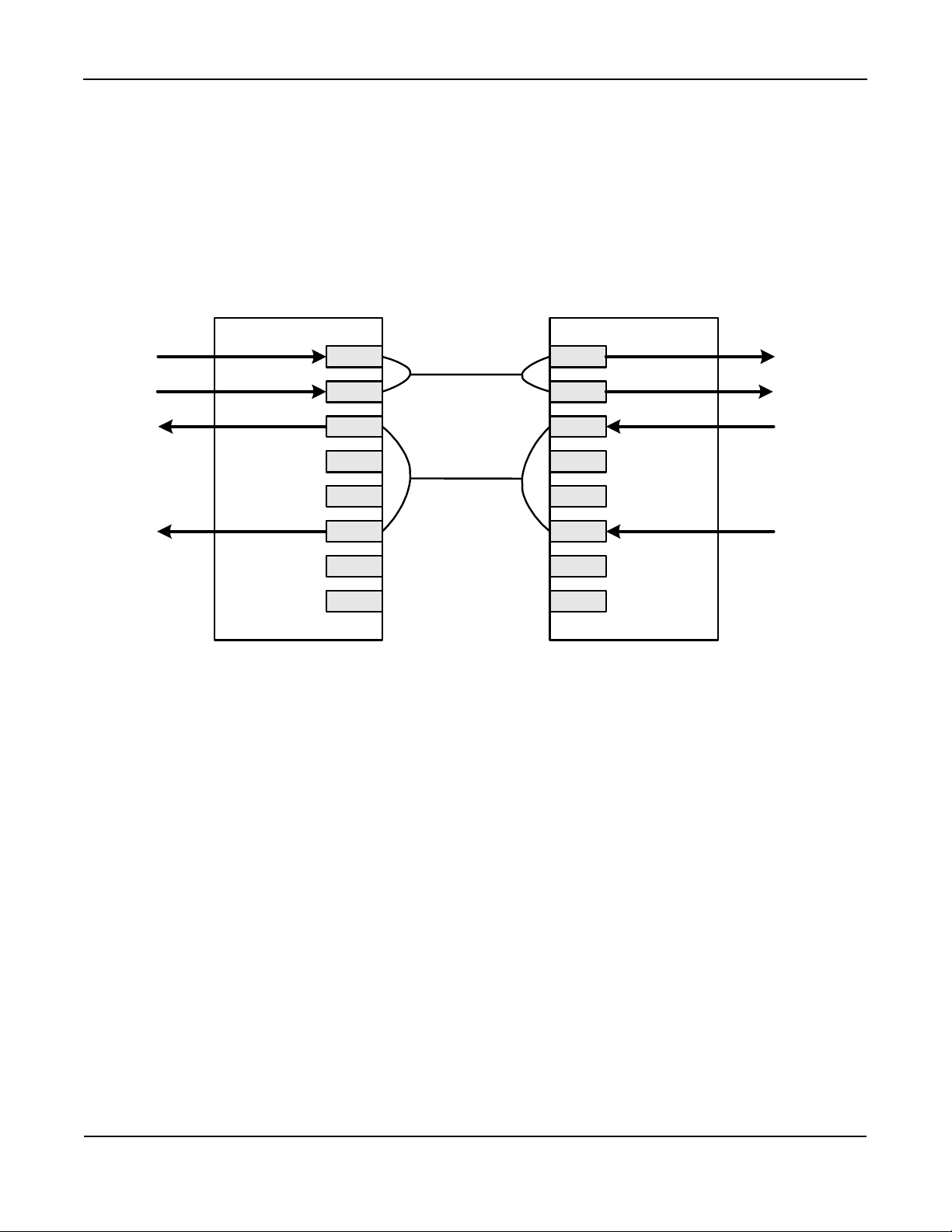
Micrel, Inc. KS8993M/ML/MI
Straight Cable
A straight cable connects an MDI device to an MDI-X device, or an MDI-X device to an MDI device. The following
diagram depicts a typical straight cable connection between a NIC card (MDI) and a switch, or hub (MDI-X).
10/100 Ethernet
Media Dependent Interface
1
2
3
4
Receive Pair
5
6
7
8
Modular Connector
(RJ-45)
NIC
Straight
Cable
10/100 Ethernet
Media Dependent Interface
1
Receive PairTransmit Pair
2
3
4
Transmit Pair
5
6
7
8
Modular Connector
(RJ-45)
HUB
(Repeater or Switch)
April 2005
Figure 1. Typical Straight Cable Connection
23 M9999-041205
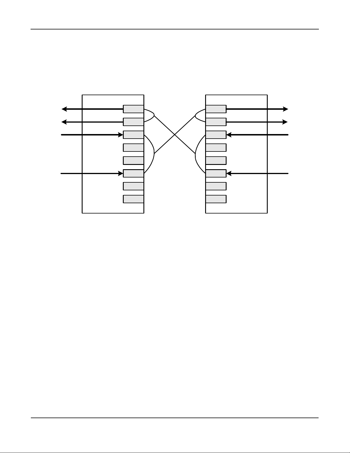
Micrel, Inc. KS8993M/ML/MI
Crossover Cable
A crossover cable connects an MDI device to another MDI device, or an MDI-X device to another MDI-X device.
The following diagram shows a typical crossover cable connection between two switches or hubs (two MDI-X
devices).
10/100 Ethernet
Media Dependent Interface
1
Receive Pair Receive Pair
2
3
4
Transmit Pair
5
6
7
8
Modular Connector (RJ-45)
HUB
(Repeater or Switch)
Crossover
Cable
10/100 Ethernet
Media Dependent Interface
1
2
3
4
Transmit Pair
5
6
7
8
Modular Connector (RJ-45)
HUB
(Repeater or Switch)
Figure 2. Typical Crossover Cable Connection
Auto Negotiation
The KS8993M conforms to the auto negotiation protocol as described by the 802.3 committee. Auto negotiation
allows unshielded twisted pair (UTP) link partners to select the best common mode of operation. In auto
negotiation, the link partners advertise capabilities across the link to each other. If auto negotiation is not
supported or the link partner to the KS8993M is forced to bypass auto negotiation, then the mode is set by
observing the signal at the receiver. This is known as parallel mode because while the transmitter is sending auto
negotiation advertisements, the receiver is listening for advertisements or a fixed signal protocol.
The link setup is shown in the following flow diagram.
April 2005
24 M9999-041205
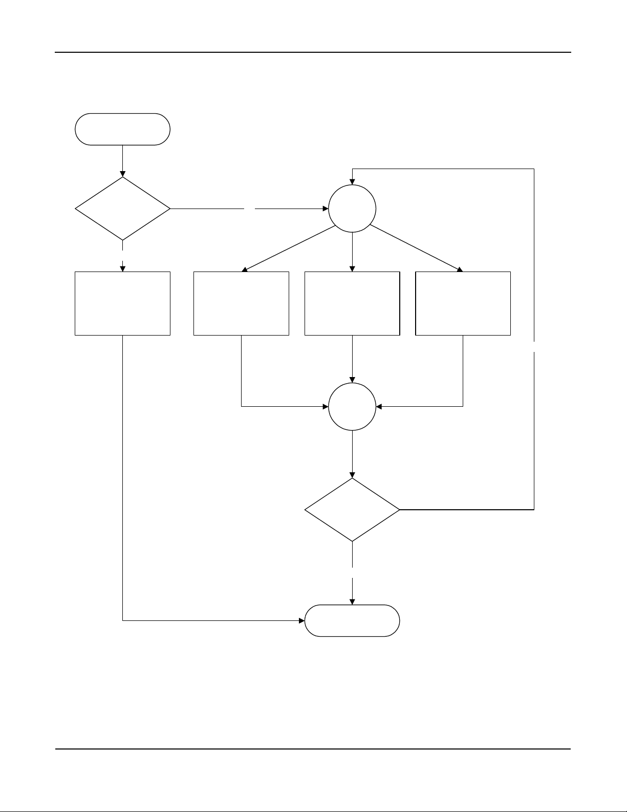
Micrel, Inc. KS8993M/ML/MI
Start Auto Negotiation
Force Link Setting
Ye
s
Bypass Auto Negotiation
and Set Link Mode
N
o
Attempt Auto
Negotiation
Parallel
Operation
Listen for 100BASE-TX
Idles
Join
Flow
Listen for 10BASE-T Link
Pulses
No
April 2005
Link Mode Set ?
Yes
Link Mode Set
Figure 3. Auto Negotiation and Parallel Operation
25 M9999-041205

Micrel, Inc. KS8993M/ML/MI
Functional Overview: MAC and Switch
Address Lookup
The internal lookup table stores MAC addresses and their associated information. It contains a 1K uni-cast
address table plus switching information. The KS8993M is guaranteed to learn 1K addresses and distinguishes
itself from hash-based lookup tables, which depending on the operating environment and probabilities, may not
guarantee the absolute number of addresses that can be learned.
Learning
The internal lookup engine will update its table with a new entry if the following conditions are met:
1. The received packet's SA does not exist in the lookup table.
2. The received packet is good; the packet has no receiving errors, and is of legal length.
The lookup engine will insert the qualified SA into the table, along with the port number and time stamp. If the
table is full, the last entry of the table will be deleted to make room for the new entry.
Migration
The internal lookup engine also monitors whether a station has moved. If so, it will update the table accordingly.
Migration happens when the following conditions are met:
1. The received packet's SA is in the table but the associated source port information is different.
2. The received packet is good; the packet has no receiving errors, and is of legal length.
The lookup engine will update the existing record in the table with the new source port information.
Aging
The lookup engine will update the time stamp information of a record whenever the corresponding SA appears.
The time stamp is used in the aging process. If a record is not updated for a period of time, the lookup engine will
remove the record from the table. The lookup engine constantly performs the aging process and will continuously
remove aging records. The aging period is about 200 seconds. This feature can be enabled or disabled through
Global Register 3 (0x03).
Forwarding
The KS8993M will forward packets using the algorithm that is depicted in the following flowcharts. Figure 4 shows
stage one of the forwarding algorithm where the search engine looks up the VLAN ID, static table, and dynamic
table for the destination address, and comes up with “port to forward 1” (PTF1). PTF1 is then further modified by
spanning tree, IGMP snooping, port mirroring, and port VLA processes to come up with “port to forward 2”
(PTF2), as shown in Figure 5. The packet is sent to PTF2.
April 2005
26 M9999-041205

Micrel, Inc. KS8993M/ML/MI
Start
PTF1= NULL
Search complete.
Get PTF1 from
Static MAC Table
Search complete.
Get PTF1 from
Dynamic MAC
Table
NO
FOUND
FOUND
VLAN ID
Valid?
YES
Search Static
Table
NOT
FOUND
Dynamic Table
Search
NOT
FOUND
- Search VLAN table
- Ingress VLAN filtering
- Discard NPVID check
This search is based on
DA or DA+FID
This search is based on
DA+FID
April 2005
Search complete.
Get PTF1 from
VLAN Table
PTF1
Figure 4. Destination Address Lookup Flow Chart, Stage 1
27 M9999-041205

Micrel, Inc. KS8993M/ML/MI
PTF1
- Check receiving port's receive enable bit
Spanning Tree
Process
IGMP Process
- Check destination port's transmit enable bit
- Check whether packets are special (BPDU
or specified)
- Applied to MAC #1 and MAC #2
- MAC #3 is reserved for
microprocessor
- IGMP will be forwarded to port 3
- RX Mirror
Port Mirror
Process
Port VLAN
Membership
Check
PTF2
Figure 5. Destination Address Resolution Flow Chart, Stage 2
- TX Mirror
- RX or TX Mirror
- RX and TX Mirror
The KS8993M will not forward the following packets:
1. Error packets. These include framing errors, FCS errors, alignment errors, and illegal size packet errors.
2. 802.3x pause frames. The KS8993M will intercept these packets and perform the appropriate actions.
3. "Local" packets. Based on destination address (DA) lookup. If the destination port from the lookup table
matches the port where the packet was from, the packet is defined as "local."
April 2005
28 M9999-041205

Micrel, Inc. KS8993M/ML/MI
Switching Engine
The KS8993M features a high-performance switching engine to move data to and from the MACs’ packet buffers.
It operates in store and forward mode, while the efficient switching mechanism reduces overall latency.
The KS8993M has a 32kB internal frame buffer. This resource is shared between all three ports. The buffersharing mode can be programmed through Global Register 2 (0x02). In one mode, ports are allowed to use any
free buffers in the buffer pool. In the second mode, each port is only allowed to use one third of the total buffer
pool. There are a total of 250 buffers available. Each buffer is sized at 128B.
MAC Operation
The KS8993M strictly abides by IEEE 802.3 standards to maximize compatibility.
Inter Packet Gap (IPG)
If a frame is successfully transmitted, the 96 bits time IPG is measured between the two consecutive MTXEN. If
the current packet is experiencing collision, the 96 bits time IPG is measured from MCRS and the next MTXEN.
Back-Off Algorithm
The KS8993M implements the IEEE standard 802.3 binary exponential back-off algorithm, and optional
"aggressive mode" back-off. After 16 collisions, the packet will be optionally dropped depending on the chip
configuration in Global Register 3 (0x03)
Late Collision
If a transmit packet experiences collisions after 512 bit times of the transmission, the packet will be dropped.
Illegal Frames
The KS8993M discards frames less than 64 bytes and can be programmed to accept frames up to 1536 bytes in
Global Register 4 (0x04). For special applications, the KS8993M can also be programmed to accept frames up to
1916 bytes in the same global register. Since the KS8993M supports VLAN tags, the maximum sizing is adjusted
when these tags are present. See the EEPROM section for programming options.
Flow Control
The KS8993M supports standard 802.3x flow control frames on both transmit and receive sides.
On the receive side, if the KS8993M receives a pause control frame, the KS8993M will not transmit the next
normal frame until the timer, specified in the pause control frame, expires. If another pause frame is received
before the current timer expires, the timer will be updated with the new value in the second pause frame. During
this period (being flow controlled), only flow control packets from the KS8993M will be transmitted.
On the transmit side, the KS8993M has intelligent and efficient ways to determine when to invoke flow control.
The flow control is based on availability of the system resources, including available buffers, available transmit
queues and available receive queues.
The KS8993M will flow control a port, which just received a packet, if the destination port resource is being used
up. The KS8993M will issue a flow control frame (XOFF), containing the maximum pause time defined in IEEE
standard 802.3x. Once the resource is freed up, the KS8993M will send out the other flow control frame (XON)
with zero pause time to turn off the flow control (turn on transmission to the port). A hysteresis feature is provided
to prevent the flow control mechanism from being activated and deactivated too many times.
The KS8993M will flow control all ports if the receive queue becomes full.
Half-Duplex Backpressure
A half-duplex backpressure option (Note: not in IEEE 802.3 standards) is also provided. The activation and
deactivation conditions are the same as the above in full duplex mode. If backpressure is required, the KS8993M
will send preambles to defer the other stations' transmission (carrier sense deference). To avoid jabber and
excessive deference defined in 802.3 standard, after a certain time it will discontinue the carrier sense but it will
raise the carrier sense quickly. This short silent time (no carrier sense) is to prevent other stations from sending
April 2005
29 M9999-041205

Micrel, Inc. KS8993M/ML/MI
out packets and keeps other stations in carrier sense deferred state. If the port has packets to send during a
backpressure situation, the carrier sense type back pressure will be interrupted and those packets will be
transmitted instead. If there are no more packets to send, carrier sense type backpressure will be active again
until switch resources free up. If a collision occurs, the binary exponential back-off algorithm is skipped and carrier
sense is generated immediately, reducing the chance of further colliding and maintaining carrier sense to prevent
reception of packets.
To ensure no packet loss in 10 BASE-T or 100 BASE-TX half duplex modes, the user must enable the following:
1. Aggressive back off (Global Register 3 (0x03), bit 0 or external strap-in pin SMAC = high)
2. No excessive collision drop (Global Register 4 (0x04), bit 3 or external strap-in pin SMAC = high)
These bits are not set as defaults because this is not the IEEE standard.
Broadcast Storm Protection
The KS8993M has an intelligent option to protect the switch system from receiving too many broadcast packets.
Broadcast packets will be forwarded to all ports except the source port, and thus use too many switch resources
(bandwidth and available space in transmit queues). The KS8993M has the option to include “multicast packets”
for storm control. The broadcast storm rate parameters are programmed globally, and can be enabled or disabled
on a per port basis. The rate is based on a 67ms interval for 100BT and a 500ms interval for 10BT. At the
beginning of each interval, the counter is cleared to zero, and the rate limit mechanism starts to count the number
of bytes during the interval. The rate definition is described in Global Register 6 (0x06) and 7 (0x07). The default
setting for registers 6 and 7 is 0x63, which is 99 decimal. This is equal to a rate of 1%, calculated as follows:
148,800 frames/sec * 67ms/interval * 1% = 99 frames/interval (approx.) = 0x63
MII Interface Operation
The MII is specified by the IEEE 802.3 standards committee and provides a common interface between physical
layer and MAC layer devices. The MII Interface provided by the KS8993M is connected to the device’s third MAC.
The interface contains two distinct groups of signals: one for transmission and the other for reception. The
following table describes the signals used in the MII interface.
KS8993M PHY-Mode Connections KS8993M MAC-Mode Connections
External MAC
Controller Signals
MTXEN SMTXEN Transmit enable MTXEN SMRXDV
MTXER SMTXER Transmit error MTXER (not used)
MTXD3 SMTXD[3] Transmit data bit 3 MTXD3 SMRXD[3]
MTXD2 SMTXD[2] Transmit data bit 2 MTXD2 SMRXD[2]
MTXD1 SMTXD[1] Transmit data bit 1 MTXD1 SMRXD[1]
MTXD0 SMTXD[0] Transmit data bit 0 MTXD0 SMRXD[0]
MTXC SMTXC Transmit clock MTXC SMRXC
MCOL SCOL Collision detection MCOL SCOL
MCRS SCRS Carrier sense MCRS SCRS
MRXDV SMRXDV Receive data valid MRXDV SMTXEN
MRXER (not used) Receive error MRXER SMTXER
MRXD3 SMRXD[3] Receive data bit 3 MRXD3 SMTXD[3]
MRXD2 SMRXD[2] Receive data bit 2 MRXD2 SMTXD[2]
MRXD1 SMRXD[1] Receive data bit 1 MRXD1 SMTXD[1]
MRXD0 SMRXD[0] Receive data bit 0 MRXD0 SMTXD[0]
MRXC SMRXC Receive clock MRXC SMTXC
KS8993M
PHY Signals
Pin
Descriptions
Table 3. MII Signals
External
PHY Signals
KS8993M
MAC Signals
April 2005
30 M9999-041205

Micrel, Inc. KS8993M/ML/MI
The MII interface operates in either PHY mode or MAC mode. The interface is a nibble wide data interfaces and
therefore run at ¼ the network bit rate (not encoded). Additional signals on the transmit side indicate when data is
valid or when an error occurs duri ng transmis sion. Likewi se, the receive side has indicators that convey when the
data is valid and without physical layer errors. For half duplex operation there is a signal that indicates a collision
has occurred during transmission.
Note that the signal MRXER is not provided on the interface for PHY mode operation and the signal MTXER is
not provided on the interface for MAC mode operation. Normally MRXER would indicate a receive error coming
from the physical layer device. MTXER would indicate a transmit error from the MAC device. These signals are
not appropriate for this configuration. For PHY mode operation, if the device interfacing with the KS8993M has an
MRXER pin, it should be tied low. For MAC mode operation, if the device interfacing with the KS8993M has an
MTXER pin, it should be tied low.
SNI (7-Wire) Operation
The serial network interface (SNI) or 7-wire is compatible with some controllers used for network layer protocol
processing. In SNI mode, the KS8993M acts like a PHY and the external controller functions as the MAC. The
KS8993M can interface directly with external controllers using the 7-wire interface. These signals are divided into
two groups, one for transmission and the other for reception. The signals involved are described in the following
table.
Pin Descriptions
Transmit enable TXEN SMTXEN
Serial transmit data TXD SMTXD[0]
Transmit clock TXC SMTXC
Collision detection COL SCOL
Carrier sense CRS SMRXDV
Serial receive data RXD SMRXD[0]
Receive clock RXC SMRXC
External MAC
Controller Signals
Table 4. SNI Signals
KS8993M
PHY Signals
The SNI interface is a bit wide data interface and therefore runs at the network bit rate (not encoded). An
additional signal on the transmit side indicates when data is valid. Similarly, the receive side has an indicator that
conveys when the data is valid.
For half duplex operation, the KS8993M’s SCOL signal is used to indicate that a collision has occurred during
transmission.
MII Management Interface (MIIM)
The KS8993M supports the IEEE 802.3 MII Management Interface, also known as the Management Data
Input/Output (MDIO) Interface. This interface allows upper-layer devices to monitor and control the states of the
KS8993M. An external device with MDC/MDIO capability can be used to read the PHY status or configure the
PHY settings. Further details on the MIIM interface can be found in section 22.2.4.5 of the IEEE 802.3
specification.
April 2005
31 M9999-041205

Micrel, Inc. KS8993M/ML/MI
The MIIM interface consists of the following:
A physical connection that incorporates the data line (MDIO) and the clock line (MDC).
A specific protocol that operates across the aforementioned physical connection that allows an external
controller to communicate with the KS8993M device.
Access to a set of six 16-bits registers, consisting of standard MIIM registers [0:5].
The following table depicts the MII Management Interface frame format.
Preamble
Read
Write
32 1’s 01 10 xx0AA RRRRR Z0 DDDDDDDD_DDDDDDDD Z
32 1’s 01 01 xx0AA RRRRR 10 DDDDDDDD_DDDDDDDD Z
Start of
Frame
Read/Write
OP Code
Table 5. MII Management Interface Frame Format
PHY
Address
Bits [4:0]
REG
Address
Bits [4:0]
TA Data
Bits [15:0]
Idle
For the KS8993M, MIIM register access is selected when bit 2 of the PHY address is set to ‘0’. PHY address bits
[4:3] are not defined for MIIM register access, and hence can be set to either 0’s or 1’s in read/write operation.
Serial Management Interface (SMI)
The SMI is the KS8993M non-standard MIIM interface that provides access to all KS8993M configuration
registers. This interface allows an external device to completely monitor and control the states of the KS8993M.
The SMI interface consists of the following:
A physical connection that incorporates the data line (MDIO) and the clock line (MDC).
A specific protocol that operates across the aforementioned physical connection that allows an external
controller to communicate with the KS8993M device.
Access to all KS8993M configuration registers. Registers access includes the Global, Port and
Advanced Control Registers 0-127 (0x00 – 0x7F), and indirect access to the standard MIIM registers
[0:5].
The following table depicts the SMI frame format.
Preamble
Read
Write
32 1’s 01 10 RR1xx RRRRR Z0 0000_0000_DDDD_DDDD Z
32 1’s 01 01 RR1xx RRRRR 10 xxxx_xxxx_DDDD_D DDD Z
Start of
Frame
Read/Write
OP Code
Table 6. Serial Management Interface (SMI) Frame Format
PHY
Address
Bits [4:0]
REG
Address
Bits [4:0]
TA Data
Bits [15:0]
Idle
For the KS8993M, SMI register access is selected when bit 2 of the PHY address is set to ‘1’. PHY address bits
[1:0] are not defined for SMI register access, and hence can be set to either 0’s or 1’s in read/write operation.
To access the KS8993M registers 0-127 (0x00 – 0x7F), the following applies:
PHYAD[4:3] and REGAD[4:0] are concatenated to form the 7-bits address; that is, {PHYAD[4:3],
REGAD[4:0]} = bits [6:0] of the 7-bits address.
April 2005
32 M9999-041205

Micrel, Inc. KS8993M/ML/MI
Registers are 8 data bits wide. For read operation, data bits [15:8] are read back as 0’s. For write
operation, data bits [15:8] are not defined, and hence can be set to either 0’s or 1’s.
SMI register access is the same as the MIIM register access, except for the register access requirements
presented in this section.
Advanced Switch Functions
Spanning Tree Support
To support spanning tree, port 3 is the designated port for the processor.
The other ports (port 1 and port 2) can be configured in one of the five spanning tree states via “transmit enable”,
“receive enable” and “learning disable” register settings in registers 18 and 34 for ports 1 and 2, respectively. The
following description shows the port setting and software actions taken for each of the five spanning tree states.
Disable state:
Learning is disabled.
Port setting:
“transmit enable = 0, receive enable = 0, learning disable =1”
Software action:
Blocking state:
Learning is disabled.
Port setting:
“transmit enable = 0, receive enable = 0, learning disable =1”
Software action:
Listening state:
Learning is disabled.
Port setting:
“transmit enable = 0, receive enable = 0, learning disable =1”
The port should not forward or receive any packets.
The processor should not send
to the processor (packets that match some entries in the “static MAC table” with “overriding bit”
set) and the processor should discard those packets. Note: processor is connected to port 3 via
MII interface. Address learning is disabled on the port in this state.
Only packets to the processor are forwarded.
The processor should not send
program the “Static MAC table” with the entries that it needs to receive (e.g. BPDU packets). The
“overriding” bit should also be set so that the switch will forward those specific packets to the
processor. Address learning is disabled on the port in this state.
Only packets to and from the processor are forwarded.
any packets to the port. The switch may still send specific packets
any packets to the port(s) in this state. The processor should
Software action:
The processor should program the “Static MAC table” with the entries that it needs to receive
(e.g., BPDU packets). The “overriding” bit should be set so that the switch will forward those
specific packets to the processor. The processor may send packets to the port(s) in this state,
see “Special Tagging Mode” for details. Address learning is disabled on the port in this state.
Learning state:
Learning is enabled.
Port setting:
April 2005
“transmit enable = 0, receive enable = 0, learning disable = 0”
Only packets to and from the processor are forwarded.
33 M9999-041205

Micrel, Inc. KS8993M/ML/MI
Software action:
The processor should program the “Static MAC table” with the entries that it needs to receive
(e.g., BPDU packets). The “overriding” bit should be set so that the switch will forward those
specific packets to the processor. The processor may send packets to the port(s) in this state,
see “Special Tagging Mode” for details. Address learning is enabled on the port in this state.
Forwarding state:
Packets are forwarded and received normally.
Learning is enabled.
Port setting:
“transmit enable = 1, receive enable = 1, learning disable = 0”
Software action:
The processor should program the “Static MAC table” with the entries that it needs to receive
(e.g., BPDU packets). The “overriding” bit should be set so that the switch will forward those
specific packets to the processor. The processor may send packets to the port(s) in this state,
see “Special Tagging Mode” for details. Address learning is enabled on the port in this state.
Upstream Special Tagging Mode
Upstream Special Tagging Mode is designed for spanning tree protocol IGMP snooping and is flexible for use in
other applications. The Upstream Special Tagging Mode, similar to 802.1Q, requires software to change network
drivers to modify/strip/interpret the special tag. This mode is enabled by setting both register 11 bit 0 and register
48 bit 2 to “1”.
802.1Q Tag Format Special Tag Format
TPID (tag protocol identifier, 0x8100) + TCI.
Table 7. Upstream Special Tagging Mode Format
STPID (special tag identifier, 0x810 +
4 bit for “port mask”) + TCI
The STPID is only seen and used by the port 3 interface, which should be connected to a processor.
The KS8993M uses a non-zero “port mask” to bypass the lookup result and override any port setting, regardless
of port states (disable, blocking, listening, learning).
For packets from regular ports (port 1 & port 2) to port 3, the port mask is used to tell the processor which port the
packets were received on, defined as follows:
“0001” from port 1
“0010” from port 2
No port mask values, other than the previous two defined ones, should be received in Upstream Special Tagging
Mode. The egress rules are defined as follows:
Ingress Packets Egress Action to Tag Field
- Modify TPID to 0x810 + “port mask”, which indicates source port.
Tagged with 0x8100 + TCI
Not tagged.
Table 8. STPID Egress Rules (Switch Port 3 to Processor)
- No change to TCI if VID is not null
- Replace null VID with ingress port VID
- Recalculate CRC
- Insert TPID to 0x810 + “port mask”, which indicates source port
– Insert TCI with ingress port VID
- Recalculate CRC
April 2005
34 M9999-041205

Micrel, Inc. KS8993M/ML/MI
IGMP Support
For IGMP support in layer 2, the KS8993M provides two components:
“IGMP” Snooping
The KS8993M will trap IGMP packets and forward them only to the processor (port 3). The IGMP packets are
identified as IP packets (either Ethernet IP packets, or IEEE 802.3 SNAP IP packets) with IP version = 0x4 and
protocol version number = 0x2.
“Multicast Address Insertion” in the Static MAC Table
Once the multicast address is programmed in the Static MAC Table, the multicast session will be trimmed to the
subscribed ports, instead of broadcasting to all ports.
To enable IGMP support, set register 5 bit 6 to “1”. Also, “Special Tagging Mode” needs to be enabled, so that the
processor knows which port the IGMP packet was received on. This is achieved by setting both register 11 bit 0
and register 48 bit 2 to “1.”
Port Mirroring Support
KS8993M supports “Port Mirroring” comprehensively as:
1. “receive only” mirror on a port
example, port 1 is programmed to be “receive sniff” and port 3 is programmed to be the “sniffer port”. A packet
received on port 1 is destined to port 2 after the internal lookup. The KS8993M will forward the packet to both port
2 and port 3. The KS8993M can optionally forward even “bad” received packets to the “sniffer port”.
2. “transmit only” mirror on a port
For example, port 1 is programmed to be “transmit sniff” and port 3 is programmed to be the “sniffer port”. A
packet received on port 2 is destined to port 1 after the internal lookup. The KS8993M will forward the packet to
both port 1 and port 3.
3. “receive and transmit” mirror on two ports
be mirrored on the sniffer port. To turn on the “AND” feature, set register 5 bit 0 to “1”. For example, port 1 is
programmed to be “receive sniff”, port 2 is programmed to be “transmit sniff” and port 3 is programmed to be the
“sniffer port”. A packet received on port 1 is destined to port 2 after the internal lookup. The KS8993M will forward
the packet to both port 2 and port 3.
Multiple ports can be selected to be “receive sniff” or “transmit sniff”. And any port can be selected to be the
“sniffer port”. All these per port features can be selected through registers 17, 33 and 49 for ports 1, 2 and 3,
respectively.
IEEE 802.1Q VLAN Support
The KS8993M supports 16 active VLANs out of the 4096 possible VLANs specified in the IEEE 802.1Q
specification. KS8993M provides a 16-entries VLAN Table, which converts the 12-bits VLAN ID (VID) to the 4-bits
Filter ID (FID) for address lookup. If a non-tagged or null-VID-tagged packet is received, the ingress port default
VID is used for lookup. In VLAN mode, the lookup process starts with VLAN Table lookup to determine whether
the VID is valid. If the VID is not valid, the packet will be dropped and its address will not be learned. If the VID is
valid, the FID is retrieved for further lookup. The FID + Destination Address (FID+DA) are used to determine the
destination port. The FID + Source Address (FID+SA) are used for address learning.
All the packets received on the port will be mirrored on the sniffer port. For
All the packets transmitted on the port will be mirrored on the sniffer port.
All the packets received on port A and transmitted on port B will
April 2005
35 M9999-041205

Micrel, Inc. KS8993M/ML/MI
DA found in
Static MAC
Table?
No Don’t care Don’t care No
No Don’t care Don’t care Yes
Yes 0 Don’t care Don’t care
Yes 1 No No
Yes 1 No Yes
Yes 1 Yes Don’t care
FID+SA found in Dynamic
MAC Table?
No Learn and add FID+SA to the Dynamic MAC Address Table
Yes Update time stamp
Use FID flag? FID match?
Table 9. FID+DA Lookup in VLAN Mode
Action
Table 10. FID+SA Lookup in VLAN Mode
DA+FID
found in
Dynamic
MAC Table?
Action
Broadcast to the membership ports
defined in the
Send to the destination port defined in the
Dynamic MAC Address Table
Send to the destination port(s) defined in
Static MAC Address Table
the
Broadcast to the membership ports
defined in the
Send to the destination port defined in the
Dynamic MAC Address Table
Send to the destination port(s) defined in
Static MAC Address Table
the
VLAN Tabl
VLAN Table
bits [18:16]
bits [53:52]
bits [50:48]
e bits [18:16]
bits [53:52]
bits [50:48]
Advanced VLAN features, such as “Ingress VLAN filtering” and “Discard Non PVID packets” are also supported
by the KS8993M. These features can be set on a per port basis, and are defined in register 18, bit 6 and bit 5,
respectively for port 1.
QoS Priority Support
This feature provides Quality of Service (QoS) for applications, such as VoIP and video conferencing. The
KS8993M per port transmit queue could be split into two priority queues: a high priority queue and a low priority
queue. Bit 0 of registers 16, 32 and 48 is used to enable split transmit queues for ports 1, 2 and 3, respectively.
Optionally, the Px_TXQ2 strap-in pins can be used to enable this feature. With split transmit queues, high priority
packets will be placed in the high priority queue and low priority packets will be placed in the low priority queue.
For split transmit queues, the KS8993M provides four priority schemes:
1. “Transmit all high priority packets before low priority packets;” i.e. a low priority packet could be transmitted
only when the high priority queue is empty
2. “Transmit high priority packets and low priority packets at 10:1 ratio;” i.e. transmit a low priority packet after
every 10 high priority packets are transmitted, if both queues are busy
3. “Transmit high priority packets and low priority packets at 5:1 ratio”
4. “Transmit high priority packets and low priority packets at 2:1 ratio”
If a port's transmit queue is not split, both high priority packets and low priority packets have equal priority in the
transmit queue. Register 5 bits [3:2] are used to select the desired priority scheme. Optionally, the PRSEL1 and
PRSEL0 strap-in pins can be used.
April 2005
36 M9999-041205

Micrel, Inc. KS8993M/ML/MI
Port-Based Priority
With port based priority, each ingress port can be individually classified as a high priority receiving port. All
packets received at the high priority receiving port are marked as high priority, and will be sent to the high priority
transmit queue if the corresponding transmit queue is split. Bit 4 of registers 16, 32 and 48 is used to enable port
based priority for ports 1, 2 and 3, respectively. Optionally, the Px_PP strap-in pins can be used to enable this
feature.
802.1p-Based Priority
For 802.1p based priority, the KS8993M will examine the ingress (incoming) packets to determine whether they
are tagged. If tagged, the 3-bits priority field in the VLAN tag is retrieved and compared against the “priority base”
value, specified by register 2 bits [6:4]. The “priority base” value is programmable; its default value is 0x4.
The following figure illustrates how the 802.1p priority field is embedded in the 802.1Q VLAN tag.
Bytes
802.1q VLAN Tag
866 2
Preamble DA TCI
Bits
SA VPID
16 3 12
Tagged Packet Type
(8100 for Ethernet)
2
802.1p
2 46-1500 4
length LLC Data FCS
1
VLAN ID
CFI
Figure 6. 802.1p Priority Field Format
If an ingress packet has an equal or higher priority value than the "priority base" value, the packet will be placed in
the high priority transmit queue if the corresponding transmit queue is split. 802.1p based priority is enabled by bit
5 of registers 16, 32 and 48 for ports 1, 2 and 3, respectively. Optionally, the Px_1PEN strap-in pins can be used
to enable this feature.
The KS8993M provides the option to insert or remove the priority tagged frame's header at each individual egress
port. This header, consisting of the 2 bytes VLAN Protocol ID (VPID) and the 2 bytes Tag Control Information field
(TCI), is also refer to as the 802.1Q VLAN Tag.
Tag Insertion is enabled by bit 2 of registers 16, 32 and 48 for ports 1, 2 and 3, respectively. Optionally, the
Px_TAGINS strap-in pins can be used to enable this feature. At the egress port, untagged packets are tagged
with the ingress port’s default tag. The default tags are programmed in register sets {19,20}, {35,36} and {51,52}
for ports 1, 2 and 3, respectively. The KS8993M will not add tags to already tagged packets.
Tag Removal is enabled by bit 1 of registers 16, 32 and 48 for ports 1, 2 and 3, respectively. Optionally, the
Px_TAGRM strap-in pins can be used to enable this feature. At the egress port, tagged packets will have their
802.1Q VLAN Tags removed. The KS8993M will not modify untagged packets.
The CRC is recalculated for both tag insertion and tag removal.
802.1p Priority Field Re-mapping is a QoS feature that allows the KS8993M to set the “User Priority Ceiling” at
any ingress port. If the ingress packet’s priority field has a higher priority value than the default tag’s priority field
of the ingress port, the packet’s priority field is replaced with the default tag’s priority field. The “User Priority
Ceiling” is enabled by bit 3 of registers 16, 32 and 48 for ports 1, 2 and 3, respectively.
DiffServ-Based Priority
DiffServ-based priority uses registers 96 to 103. More details are provided at the beginning of the Advanced
Control Registers section.
April 2005
37 M9999-041205

Micrel, Inc. KS8993M/ML/MI
Rate Limiting Support
The KS8993M supports hardware rate limiting independently on the “receive side” and on the “transmit side” on a
per port basis. Rate limiting is supported in both priority and non-priority environment. The rate limit starts from 0
kbps and goes up to the line rate in steps of 32 kbps. The KS8993M uses “one second” as the rate limiting
interval. At the beginning of each interval, the counter is cleared to zero, and the rate limit mechanism starts to
count the number of bytes during the interval.
On the “receive side”, if the number of bytes exceeds the programmed limit, the switch will stop receiving packets
on the port until the “one second” interval expires. Flow control can be enabled to prevent packet loss. If the rate
limit is programmed greater than or equal to 128 kbps and the byte counter is 8 Kbytes below the limit, flow
control will be triggered. If the rate limit is programmed lower than 128 kbps and the byte counter is 2 Kbytes
below the limit, flow control will also be triggered.
On the “transmit side”, if the number of bytes exceeds the programmed limit, the switch will stop transmitting
packets on the port until the “one second” interval expires.
If priority is enabled, the KS8993M can be programmed to support different rate limits for high priority packets and
low priority packets.
Configuration Interface
The KS8993M can operate as both a managed switch and an unmanaged switch.
In unmanaged mode, the KS8993M is typically programmed using an EEPROM. If no EEPROM is present, the
KS8993M is configured using its default register settings. Some defaults settings are configured via strap-in pin
options. The strap-in pins are indicated in the “KS8993M Pin Description and I/O Assignment” table.
2
I
C Master Serial Bus Configuration
With an additional I
2
C (“2-wire”) EEPROM, the KS8993M can perform more advanced switch features like
“broadcast storm protection” and “rate control” without the need of an external processor.
For KS8993M I
2
C Master configuration, the EEPROM stores the configuration data for register 0 to register 109
(as defined in the KS8993M register map) with the exception of the “Read Only” status registers. After the deassertion of reset, the KS8993M will sequentially read in the configuration data for all 110 registers, starting from
register 0. The configuration access time (t
) is less than 15 ms, as depicted in the following figure.
prgm
t
prgm
....
....
....
<15 ms
RST_N
SCL
SDA
Figure 7. KS8993M EEPROM Configuration Timing Diagram
The following is a sample procedure for programming the KS8993M with a pre-configured EEPROM:
1. Connect the KS8993M to the EEPROM by joining the SCL and SDA signals of the respective devices. For the
KS8993M, SCL is pin 97 and SDA is pin 98.
April 2005
38 M9999-041205

Micrel, Inc. KS8993M/ML/MI
2. Enable I2C master mode by setting the KS8993M strap-in pins, PS[1:0] (pins 100 and 101, respectively) to
“00”.
3. Check to ensure that the KS8993M reset signal input, RST_N (pin 67), is properly connected to the external
reset source at the board level.
4. Program the desired configuration data into the EEPROM.
5. Place the EEPROM on the board and power up the board.
6. Assert an active-low reset to the RST_N pin of the KS8993M. After reset is de-asserted, the KS8993M will
begin reading the configuration data from the EEPROM. The KS8993M will check that the first byte read from
the EEPROM is “93”. If this value is correct, EEPROM configuration will continue. If not, EEPROM
configuration access is denied and all other data sent from the EEPROM will be ignored by the KS8993M.
The configuration access time (t
) is less than 15ms.
prgm
Note: For proper operation, check to ensure that the KS8993M PWRDN input signal (pin 36) is not asserted
during the reset operation. The PWRDN input is active low.
2
I
C Slave Serial Bus Configuration
In managed mode, the KS8993M can be configured as an I
2
C slave device. In this mode, an I2C master device
(external controller/CPU) has complete programming access to the KS8993M’s 128 registers. Programming
access includes the Global Registers, Port Registers, Advanced Control Registers and indirect access to the
“Static MAC Table”, “VLAN Table”, “Dynamic MAC Table,” and “MIB Counters.” The tables and counters are
indirectly accessed via registers 110 thru 120.
2
In I
C slave mode, the KS8993M operates like other I2C slave devices. Addressing the KS8993M’s 8 bit registers
is similar to addressing Atmel’s AT24C02 EEPROM’s memory locations. Details of I
2
C read/write operations and
related timing information can be found in the AT24C02 Datasheet.
Two fixed 8 bits device addresses are used to address the KS8993M in I
2
C slave mode. One is for read; the other
is for write. The addresses are as follow:
1011_1111 <read>
1011_1110 <write>
The following is a sample procedure for programming the KS8993M using the I
1. Enable I
2
C slave mode by setting the KS8993M strap-in pins PS[1:0] (pins 100 and 101, respectively) to “01”.
2
C slave serial bus:
2. Power up the board and assert reset to the KS8993M. After reset, the “Start Switch” bit (register 1 bit 0) will
be set to ‘0’.
3. Configure the desired register settings in the KS8993M, using the I
4. Read back and verify the register settings in the KS8993M, using the I
2
C write operation.
2
C read operation.
5. Write a ‘1’ to the “Start Switch” bit to start the KS8993M with the programmed settings.
Note: The “Start Switch” bit cannot be set to ‘0’ to stop the switch after an ‘1’ is written to this bit. Thus, it is
recommended that all switch configuration settings are programmed before the “Start Switch” bit is set to ‘1’.
Some of the configuration settings, such as “Aging enable”, “Auto Negotiation Enable”, “Force Speed” and “Power
down” can be programmed after the switch has been started.
SPI Slave Serial Bus Configuration
In managed mode, the KS8993M can be configured as a SPI slave device. In this mode, a SPI master device
(external controller/CPU) has complete programming access to the KS8993M’s 128 registers. Programming
access includes the Global Registers, Port Registers, Advanced Control Registers and indirect access to the
“Static MAC Table”, “VLAN Table”, “Dynamic MAC Table” and “MIB Counters”. The tables and counters are
indirectly accessed via registers 110 thru 120.
The KS8993M supports two standard SPI commands: ‘0000_0011’ for data read and ‘0000_0010’ for data write.
SPI multiple read and multiple write are also supported by the KS8993M to expedite register read back and
register configuration, respectively.
April 2005
39 M9999-041205

Micrel, Inc. KS8993M/ML/MI
SPI multiple read is initiated when the master device continues to drive the KS8993M SPIS_N input pin (SPI
Slave Select signal) low after a byte (a register) is read. The KS8993M internal address counter will increment
automatically to the next byte (next register) after the read. The next byte at the next register address will be
shifted out onto the KS8993M SPIQ output pin. SPI multiple read will continue until the SPI master device
terminates it by de-asserting the SPIS_N signal to the KS8993M.
Similarly, SPI multiple write is initiated when the master device continues to drive the KS8993M SPIS_N input pin
low after a byte (a register) is written. The KS8993M internal address counter will increment automatically to the
next byte (next register) after the write. The next byte that is sent from the master device to the KS8993M SDA
input pin will be written to the next register address. SPI multiple write will continue until the SPI master device
terminates it by de-asserting the SPIS_N signal to the KS8993M.
For both SPI multiple read and multiple write, the KS8993M internal address counter will wrap back to register
address zero once the highest register address is reached. This feature allows all 128 KS8993M registers to be
read, or written with a single SPI command and any initial register address.
The KS8993M is capable of supporting a 5MHz SPI bus.
The following is a sample procedure for programming the KS8993M using the SPI bus:
1. At the board level, connect the KS8993M pins as follows:
KS8993M Pin # KS8993M Signal Name External Processor Sig nal Description
99 SPIS_N SPI Slave Select
97
98
96 SPIQ
SCL
(SPIC)
SDA
(SPID)
SPI Clock
SPI Data
(Master output; Slave input)
SPI Data
(Master input; Slave output)
Table 11. KS8993M SPI Connections
2. Enable SPI slave mode by setting the KS8993M strap-in pins PS[1:0] (pins 100 and 101, respectively) to “10”.
3. Power up the board and assert reset to the KS8993M.
After reset, the “Start Switch” bit (register 1 bit 0) will be set to ‘0’.
4. Configure the desired register settings in the KS8993M, using the SPI write or multiple write command.
5. Read back and verify the register settings in the KS8993M, using the SPI read or multiple read command.
6. Write a ‘1’ to the “Start Switch” bit to start the KS8993M with the programmed settings.
Note: The “Start Switch” bit cannot be set to ‘0’ to stop the switch after an ‘1’ is written to this bit. Thus, it is
recommended that all switch configuration settings are programmed before the “Start Switch” bit is set to ‘1’.
Some of the configuration settings, such as “Aging enable”, “Auto Negotiation Enable”, “Force Speed” and “Power
down” can be programmed after the switch has been started.
The following four figures illustrate the SPI data cycles for “Write”, “Read”, “Multiple Write” and “Multiple Read”.
The read data is registered out of SPIQ on the falling edge of SPIC, and the data input on SPID is registered on
the rising edge of SPIC.
April 2005
40 M9999-041205

Micrel, Inc. KS8993M/ML/MI
SPIS_N
SPIC
SPID
SPIQ
00000010X A7 A6 A5 A4 A3 A2 A1
WRITE COMMAND WRITE ADDRESS WRITE DATA
A0
D2 D0D1D3D4D5D6D7
Figure 8. SPI Write Data Cycle
SPIS_N
SPIC
SPID
SPIQ
00000011X A7 A6 A5 A4 A3 A2 A1
READ COMMAND READ ADDRESS READ DATA
A0
D7 D6 D5 D4 D3 D2 D1 D0
Figure 9. SPI Read Data Cycle
SPIS_N
SPIC
SPID
SPIQ
SPIS_N
SPIC
SPID
SPIQ
00000010X A7 A6 A5 A4 A3 A2 A1
WRITE COMMAND WRIT E ADDRE SS Byte 1
D7 D6 D5 D4 D4 D2 D1 D0 D7 D6 D5 D4 D3 D2 D1
Byte 2 Byte 3 ... Byte N
Figure 10. SPI Multiple Write
A0
D0
D2 D0D1D3D4D5D6D7
D2 D0D1D3D4D5D6D7
April 2005
41 M9999-041205

Micrel, Inc. KS8993M/ML/MI
SPIS_N
SPIC
SPID
SPIQ
SPIS_N
SPIC
SPID
SPIQ
00000011X A7 A6 A5 A4 A3 A2 A1
READ COMMAND READ ADDRESS Byte 1
XXXXXXXXXXXXXXX
D7 D6 D5 D4 D3 D2 D1 D0 D7 D6 D5 D4 D3 D2 D1 D0
Byte 2 Byte 3 Byte N
X X X X X X X X
A0
D7 D6 D5 D4 D3 D2 D1 D0
X
XXXXXXXX
D7 D6 D5 D4 D3 D2 D1 D0
Figure 11. SPI Multiple Read
April 2005
42 M9999-041205

Micrel, Inc. KS8993M/ML/MI
Loopback Support
The KS8993M provides loopback support for remote diagnostic of failure. In loopback mode, the speed at both
PHY ports needs to be set to 100BASE-TX, and the “Priority Buffer reserve” bit needs to be set to 48 preallocated buffers per output queue. The latter is required to prevent loopback packet drops and is achieved by
setting register 4 bit 0 to ‘1’.
Bit 0 of registers 29 and 45 is used to enable loopback for ports 1 and 2, respectively.
Alternatively, the MII Management register 0, bit 14 can be used to enable loopback.
Loopback is conducted between the KS8993M’s two PHY ports. The loopback path starts at the “Originating.”
PHY ports receive inputs (RXP/RXM), wraps around at the “loopback” PHY port’s PMD/PMA, and ends at the
“Originating” PHY port’s transmit outputs (TXP/TXM). The KS8993M loopback path is illustrated in the following
figure.
April 2005
Figure 12. Loopback Path
43 M9999-041205

Micrel, Inc. KS8993M/ML/MI
MII Management (MIIM) Registers
The MIIM interface is used to access the MII PHY registers defined in this section. The SPI, I2C, and SMI
interfaces can also be used to access these registers. The latter three interfaces use a different mapping
mechanism than the MIIM interface.
As defined in the IEEE 802.3 specification, the “PHYAD” are assigned as “0x1” for PHY port 1 and “0x2” for PHY
port 2. The “REGAD” supported are 0,1,2,3,4, and 5.
Register Number Description
0x0 Basic Control Register
0x1 Basic Status Register
0x2 Physical Identifier I
0x3 Physical Identifier II
0x4 Auto-Negotiation Advertisement Register
0x5 Auto-Negotiation Link Partner Ability Register
0x6 – 0x1F Not supported
Register 0: MII Basic Control
Bit Name R/W Description Default Reference
15 Soft reset RO NOT SUPPORTED 0
14 Loopback R/W =1, Loopback mode
=0, Normal operation
13 Force 100 R/W =1, 100 Mbps
=0, 10 Mbps
12 AN enable R/W =1, Auto-negotiation enabled
=0, Auto-negotiation disabled
11 Power down R/W =1, Power down
=0, Normal operation
10 Isolate RO NOT SUPPORTED 0
9 Restart AN R/W =1, Restart auto-negotiation
=0, Normal operation
8
7 Collision test RO NOT SUPPORTED 0
6 Reserved RO 0
5 Reserved RO 0
4 Force MDI R/W =1, Force MDI (transmit on RXP / RXM pins)
Force full
duplex
R/W =1, Full duplex
=0, Half duplex
=0, Normal operation (transmit on TXP / TXM
pins)
0 Reg. 29, bit 0
Reg. 45, bit 0
0 Reg. 28, bit 6
Reg. 44, bit 6
1
0 Reg. 29, bit 3
Reg. 45, bit 3
0 Reg. 29, bit 5
Reg. 45, bit 5
0 Reg. 28, bit 5
Reg. 44, bit 5
0 Reg. 29, bit 1
Reg. 45, bit 1
April 2005
44 M9999-041205

Micrel, Inc. KS8993M/ML/MI
Register 0: MII Basic Control (continued)
Bit Name R/W Description Default Reference
3 Disable MDI X R/W =1, Disable auto MDI-X
=0, Normal operation
2
1
0 Disable LED R/W =1, Disable LED
Disable far end
fault
Disable
transmit
R/W =1, Disable far end fault detection
=0, Normal operation
R/W =1, Disable transmit
=0, Normal operation
=0, Normal operation
0 Reg. 29, bit 2
Reg. 45, bit 2
0 Reg. 29, bit 4
0 Reg. 29, bit 6
Reg. 45, bit 6
0 Reg. 29, bit 7
Reg. 45, bit 7
Register 1: MII Basic Status
Bit Name R/W Description Default Reference
15 T4 capable RO =0, Not 100 BASE-T4 capable 0
14
13
12
11
10-7 Reserved RO 0
6
5 AN complete RO =1, Auto-neg otiation complete
4 Far end fault RO =1, Far end fault detected
3 AN capable RO =1, Auto-negotiation capable
2 Link status RO =1, Link is up
1 Jabber test RO NOT SUPPORTED 0
0
100 Full
capable
100 Half
capable
10 Full
capable
10 Half
capable
Preamble
suppressed
Extended
capable
RO =1, 100BASE-TX full duplex capable
=0, Not capable of 100BASE-TX full duplex
RO =1, 100BASE-TX half duplex capable
=0, Not 100BASE-TX half duplex capable
RO =1, 10BASE-T full duplex capable
=0, Not 10BASE-T full duplex capable
RO =1, 10BASE-T half duplex capable
=0, Not 10BASE-T half duplex capable
RO NOT SUPPORTED 0
=0, Auto-negotiation not completed
=0, No far end fault detected
=0, Not auto-negotiation capable
=0, Link is down
RO =0, Not extended register capable 0
1 Always 1
1 Always 1
1 Always 1
1 Always 1
0 Reg. 30, bit 6
Reg. 46, bit 6
0 Reg. 31, bit 0
1 Reg. 28, bit 7
Reg. 44, bit 7
0 Reg. 30, bit 5
Reg. 46, bit 5
Register 2: PHYID HIGH
Bit Name R/W Description Default
15-0 PHYID high RO High order PHYID bits 0x0022
Register 3: PHYID LOW
Bit Name R/W Description Default
15-0
PHYID low RO Low order PHYID bits 0x1430
April 2005
45 M9999-041205

Micrel, Inc. KS8993M/ML/MI
Register 4: Auto-Negotiation Advertisement Ability
Bit Name R/W Description Default Reference
15 Next page RO NOT SUPPORTED 0
14 Reserved RO 0
13 Remote fault RO NOT SUPPORTED 0
12-11 Reserved RO 0
10 Pause R/W =1, Advertise pause ability
=0, Do not advertise pause ability
9 Reserved R/W 0
8 Adv 100 Full R/W =1, Advertise 100 full duplex ability
=0, Do not advertise 100 full duplex ability
7 Adv 100 Half R/W =1, Advertise 100 half duplex ability
=0, Do not advertise 100 half duplex
ability
6 Adv 10 Full R/W =1, Advertise 10 full duplex ability
=0, Do not advertise 10 full duplex ability
5 Adv 10 Half R/W =1, Advertise 10 half duplex ability
=0, Do not advertise 10 half duplex ability
4-0 Selector field RO 802.3 00001
1 Reg. 28, bit 4
Reg. 44, bit 4
1 Reg. 28, bit 3
Reg. 44, bit 3
1 Reg. 28, bit 2
Reg. 44, bit 2
1 Reg. 28, bit 1
Reg. 44, bit 1
1 Reg. 28, bit 0
Reg. 44, bit 0
Register 5: Auto-Negotiation Link Partner Ability
Bit Name R/W Description Default Reference
15 Next page RO NOT SUPPORTED 0
14 LP ACK RO NOT SUPPORTED 0
13 Remote fault RO NOT SUPPORTED 0
12-11 Reserved RO 0
10 Pause RO Link partner pause capability 0 Reg. 30, bit 4
Reg. 46, bit 4
9 Reserved RO 0
8 Adv 100 Full RO Link partner 100 full capability 0 Reg. 30, bit 3
Reg. 46, bit 3
7 Adv 100 Half RO Link partner 100 half capability 0 Reg. 30, bit 2
Reg. 46, bit 2
6 Adv 10 Full RO Link partner 10 full capability 0 Reg. 30, bit 1
Reg. 46, bit 1
5 Adv 10 Half RO Link partner 10 half capability 0 Reg. 30, bit 0
Reg. 46, bit 0
4-0 Reserved RO 00000
April 2005
46 M9999-041205

Micrel, Inc. KS8993M/ML/MI
Register Map: Switch & PHY (8 bit registers)
Global Registers
Register (Decimal) Register (Hex0 Description
0-1 0x00-0x01 Chip ID Registers
2-11 0x02-0x0B Global Control Registers
12 0x0C Reserved Register
13-15 0x0D-0x0F User Defined Registers
Port Registers
Register (Decimal) Register (Hex0 Description
16-29 0x10-0 x1D Port 1 Control Registers, including MII PHY Registers
30-31 0x1E-0x1F Port 1 Status Registers, including MII PHY Registers
32-45 0x20-0 x2D Port 2 Control Registers, including MII PHY Registers
46-47 0x2E-0x2F Port 2 Status Registers, including MII PHY Registers
48-61 0x30-0 x3D Port 3 Control Registers, including MII PHY Registers
62-63 0x3E-0x3F Port 3 Status Registers, including MII PHY Registers
64-95 0x40-0x5F Reserved
Advanced Control Registers
Register (Decimal) Register (Hex0 Description
96-103 0x60-0x67 TOS Priority Control Registers
104-109 0x68-0x6D Switch Engine’s MAC Address Registers
110-111 0x6E-0x6F Indirect Access Control Registers
112-120 0x70-0x78 Indirect Data Registers
121-122 0x79-0x7A Digital Testing Status Registers
123-124 0x7B-0x7C Digital Testing Control Registers
125-126 0x7D-0x7E Analog Testing Control Registers
127 0x7F Analog Testing Status Register
Global Registers
Register 0 (0x00): Chip ID0
Bit Name R/W Description Default
7-0 Family ID RO Chip family 0x93
April 2005
47 M9999-041205

Micrel, Inc. KS8993M/ML/MI
Register 1 (0x01): Chip ID1 / Start Switch
Bit Name R/W Description Default
7-4 Chip ID RO 0x0 is assigned to M series. (93M) 0x0
3-1 Revision ID RO Revision ID 0 Start switch RW = 1, start the chip when external pins
(PS1, PS0) = (0,1) or (1,0) or (1,1).
Note:
In (PS1, PS0) = (0, 0) mode, the chip will start
automatically after trying to read the external
EEPROM. If EEPROM does not exist, the chip will
use pin strapping and default values for all internal
registers. If EEPROM is present, the contents in the
EEPROM will be checked. The switch will check: (1)
Register 0 = 0x93, (2) Register 1 bits [7:4] = 0x0. If
this check is OK, the contents in the EEPROM will
override chip registers’ default values.
= 0, chip will not start when external pins
(PS1, PS0) = (0,1) or (1,0) or (1,1).
-
Register 2 (0x02): Global Control 0
Bit Name R/W Description Default
7 New back-off
Enable
6-4
3
2
1 Reserved R/W Reserved 0
0
802.1p base
priority
Pass flow
control packet
Buffer share
mode
Link change
age
R/W New back-off algorithm designed for UNH
1 = Enable
0 = Disable
R/W
R/W = 1, switch will not filter 802.1x “flow control” packets 0x0
R/W
R/W
Used to classify priority for incoming 802.1Q packets.
“user priority” is compared against this value.
>= : classified as high priority
< : classified as low priority
= 1, buffer pool is shared by all ports. A port can use
more buffers when other ports are not busy.
= 0, a port is only allowed to use 1/3 of the buffer
pool.
= 1, link change from “link” to “no link” will cause fast
aging (<800us) to age address table faster. After
an age cycle is complete, the age logic will return to
normal aging (about 200 sec).
Note:
If any port is unplugged, all addresses will be
automatically aged out.
0x0
0x4
0x1
0
April 2005
48 M9999-041205

Micrel, Inc. KS8993M/ML/MI
Register 3 (0x03): Global Control 1
Bit Name R/W Description Default
7 Pass all frames R/W
6
5
4
3
2 Aging enable R/W 1 = enable age function in the chip
1
0
Repeater
mode
IEEE 802.3x
Transmit
direction flow
control enable
IEEE 802.3x
Receive
direction flow
control enable
Frame Length
field check
Fast age
enable
Aggressive
back off enable
R/W 0 = normal mode
R/W = 1, will enable transmit direction flo w control feature.
R/W = 1, will enable receive directi on flow control feature.
R/W
R/W 1 = turn on fast age (800us) 0
R/W
= 1, switch all packets including bad ones. Used
solely for debugging purposes. Works in conjunction
with sniffer mode only.
1 = repeater mode (half duplex Hub mode)
= 0, will not enable transmit direction flow control
feature.
= 0, will not enable receive direction flow control
feature.
1 = will check frame length field in the IEEE packets.
If the actual length does not match, the packet will be
dropped
(for Length/Type field < 1500).
0 = disable age function in the chip
1 = enable more aggressive back off algorithm in half
duplex mode to enhance performance. This is not an
IEEE standard.
0
0
1
1
0
1
SMAC (pin
69) value
during
reset.
Register 4 (0x04): Global Control 2
Bit Name R/W Description Default
7
6
5 Back pressure
Unicast portVLAN
mismatch
discard
Multicast storm
protection
disable
Mode
R/W
R/W
R/W = 1, carrier sense based backpressure is selected
This feature is used for port-VLAN (described in reg.
17, reg. 33, …)
= 1, all packets can not cross VLAN
boundary
= 0, unicast packets (excluding
unkown/multicast/broadcast) can cross VLAN
boundary
Note: Port mirroring is not supported if this bit is set to
“0”.
= 1, “Broadcast Storm Protection” does not include
multicast packets. Only
DA = FFFFFFFFFFFF packets will be
regulated.
= 0, “Broadcast Storm Protection” includes
DA = FFFFFFFFFFFF and DA[40] = 1 packets.
= 0, collision based backpressure is selected
1
1
1
April 2005
49 M9999-041205

Micrel, Inc. KS8993M/ML/MI
Register 4 (0x04): Global Control 2 (continued)
Bit Name R/W Description Default
4
3
2
1
0
Flow control
and back
pressure fair
mode
No excessive
collision drop
Huge packet
support
Legal
Maximum
Packet size
check enable
Priority Buffer
reserve
R/W
R/W
R/W
R/W
R/W
= 1, fair mode is selected. In this mode, if a flow
control port and a non-flow control port talk to the
same destination port, packets from the non-flow
control port may be dropped. This is to prevent the
flow control port from being flow controlled for an
extended period of time.
= 0, in this mode, if a flow control port and a non-flow
control port talk to the same destination port, the flow
control port will be flow controlled. This may not be
“fair” to the flow control port.
= 1, the switch will not drop packets when 16 or more
collisions occur.
= 0, the switch will drop packets when 16 or more
collisions occur.
= 1, will accept packet sizes up to 1916 bytes
(inclusive). This bit setting will override setting from
bit 1 of the same register.
= 0, the max packet size will be determined by bit 1 of
this register.
= 0, will accept packet sizes up to 1536 bytes
(inclusive).
= 1, 1522 bytes for tagged packets, 1518 bytes for
untagged packets. Any packets larger than the
specified value will be dropped.
= 1, each output queue is pre-allocated 48 buffers,
used exclusively for high priority packets. It is
recommended to enable this when priority queue
feature is turned on.
= 0, no reserved buffers for high priority packets.
1
SMAC (pin
69) value
during
reset.
0
SMRXD0
(pin 85)
value
during
reset.
1
Register 5 (0x05): Global Control 3
Bit Name R/W Description Default
7
6
5 Reserved R/W 0
4 Reserved R/W 0
3-2
1 Reserved R/W 0
April 2005
802.1Q VLAN
enable
IGMP snoop
enable on
Switch MII
interface
Priority
Scheme select
R/W
R/W =1, IGMP snoop is enabled.
R/W 00 = always deliver hi gh priority packets first
= 1, 802.1Q VLAN mode is turned on. VLAN table
needs to set up before the operation.
= 0, 802.1Q VLAN is disabled.
All the IGMP packets will be forwarded to the Switch
MII port.
=0, IGMP snoop is disabled.
01 = deliver high/low packets at ratio 10/1
10 = deliver high/low packets at ratio 5/1
11 = deliver high/low packets at ratio 2/1
50 M9999-041205
0
0
00

Micrel, Inc. KS8993M/ML/MI
Register 5 (0x05): Global Control 3 (continued)
Bit Name R/W Description Default
0
Sniff mode
select
R./W
= 1, will do rx AND tx sniff (both source port and
destination port need to match)
= 0, will do rx OR tx sniff (Either source port or
destination port needs to match). This is the mode
used to implement rx only sniff.
0
Register 6 (0x06): Global Control 4
Bit Name R/W Description Default
7 Reserved R/W 0
6
5
4
Switch MII halfduplex mode
Switch MII flow
control enable
Switch MII
10BT
R/W = 1, enable MII interface half-duplex mode.
= 0, enable MII interface full-duplex mode.
R/W
R/W = 1, the switch interface is in 10Mbps mode
= 1, enable full-duplex flow control on Switch MII
interface.
= 0, disable full-duplex flow control on Switch MII
interface.
= 0, the switch interface is in 100Mbps mode
Pin SMRXD2
strap option.
Pull-down(0):
Full-duplex
mode
Pull-up(1):
Half-duplex
mode
Note:
SMRXD2 has
internal pulldown.
Pin SMRXD3
strap option.
Pull-down(0):
Disable flow
control
Pull- up(1):
Enable flow
control
Note:
SMRXD3 has
internal pulldown.
Pin SMRXD1
strap option.
Pull –
down(0):
Enable
100Mbps
Pull-up(1):
Enable
10Mpbs
Note:
SMRXD1 has
internal pulldown.
April 2005
51 M9999-041205

Micrel, Inc. KS8993M/ML/MI
Register 6 (0x06): Global Control 4 (continued)
Bit Name R/W Description Default
3
2-0
Null VID
replacement
Broadcast
storm
protection rate
Bit [10:8]
R/W = 1, will replace NULL VID with port VID(12 bits)
= 0, no replacement for NULL VID
R/W
This register along with the next register determines
how many “64 byte blocks” of packet data allowed on
an input port in a preset period. The period is 50ms
for 100BT or 500ms for 10BT. The default is 1%.
0
000
Register 7 (0x07): Global Control 5
Bit Name R/W Description Default
7-0
Note: Rate: 148,800 frames/sec * 67 ms/interval * 1% = 99 frames/interval (approx.) = 0x63
Broadcast
storm
protection
(1)
rate
Bit [7:0]
R/W
This register along with the previous register
determines how many “64 byte blocks” of packet data
are allowed on an input port in a preset period. The
period is 67ms for 100BT or 500ms for 10BT. The
default is 1%.
0x63
Register 8 (0x08): Global Control 6
Bit Name R/W Description Default
7-0 Factory testing R/W Reserved 0x4E
Register 9 (0x09): Global Control 7
Bit Name R/W Description Default
7-0 Factory testing R/W Reserved 0x24
Register 10 (0x0A): Global Control 8
Bit Name R/W Description Default
7-0 Factory testing R/W Reserved 0x24
Register 11 (0x0B): Global Control 9
Bit Name R/W Description Default
7 Reserved Reserved 0
6
5 Reserved R/W Reserved 0
4 Reserved RW Testing mode, must be 0 0
3 Reserved R/W Reserved 1
PHY
power
save
R/W = 1, enable PHY power save mode
= 0, disable PHY power save mode
0
April 2005
52 M9999-041205

Micrel, Inc. KS8993M/ML/MI
Register 11 (0x0B): Global Control 9 (continued)
Bit Name R/W Description Default
2 Reserved R/W Reserved 0
1 LED mode R/W
0
Special
TPID
mode
R/W
This register bit sets the LEDSEL0 selection only.
LEDSEL1 is set via strap-in pin.
Port x LED indicators, defined as below:
[LEDSEL1, LEDSEL0]
[0, 0] [0, 1]
PxLED3 ------ -----PxLED2 LINK/ACT 100LINK/ACT
PxLED1 FULL_DPX/COL 10LINK/ACT
PxLED0 SPEED FULL_DPX
[LEDSEL1, LEDSEL0]
[1, 0] [1, 1]
PxLED3 ACT -----PxLED2 LINK -----PxLED1 FULL_DPX/COL ------
PxLED0 SPEED -----Notes:
LEDSEL0 is external strap-in pin #70.
LEDSEL1 is external strap-in pin #23.
Used for direct mode forwarding from port 3. See
description in “spanning tree” functional description.
0 = disable
1 = enable
LEDSEL0
pin value
during
reset.
0
Register 12 (0x0C): Reserved Register
Bit Name R/W Description Default
7-0 Reserved Reserved 0x00
Register 13 (0x0D): User Defined Register 1
Bit Name R/W Description Default
7-0 UDR1 R/W 0x00
Register 14 (0x0E): User Defined Register 2
Bit Name R/W Description Default
7-0 UDR2 R/W 0x00
Register 15 (0x0F): User Defined Register 3
Bit Name R/W Description Default
7-0 UDR3 R/W 0x00
April 2005
53 M9999-041205

Micrel, Inc. KS8993M/ML/MI
Port Registers
The following registers are used to enable features that are assigned on a per port basis. The register bit
assignments are the same for all ports, but the address for each port is different, as indicated.
Register 16 (0x10): Port 1 Control 0
Register 32 (0x20): Port 2 Control 0
Register 48 (0x30): Port 3 Control 0
Bit Name R/W Description Default
7
6
5
4
3
2 Tag insertion R/W
Broadcast
storm
protection
enable
DiffServ priority
classification
enable
802.1p priority
classification
enable
Port-based
priority
classification
enable
User priority
ceiling
R/W
R/W
R/W
R/W
R/W
= 1, enable broadcast storm protection for
ingress packets on the port
= 0, disable broadcast storm protection
= 1, enable DiffServ priority classification for
ingress packets on port
= 0, disable DiffServ function
= 1, enable 802.1p priority classification for
ingress packets on port
= 0, disable 802.1p
= 1, ingress packets on the port will be classified
as high priority if “DiffServ” or “802.1p”
classification is not enabled or fails to classify.
= 0, ingress packets on port will be classified as
low priority if “DiffServ” or “802.1p” classification
is not enabled or fails to classify.
Note: “DiffServ”, “802.1p” and port priority can be
enabled at the same time. The OR’ed result of
802.1p and DSCP overwrites the port priority.
= 1, if the packet’s “user priority field” is greater
than the “user priority field” in the port default tag
register, replace the packet’s “user priority field”
with the “user priority field” in the port default tag
register.
= 0, do not compare and replace the packet’s
‘user priority field”
= 1, when packets are output on the port, the
switch will add 802.1p/q tags to packets without
802.1p/q tags when received. The switch will not
add tags to packets already tagged. The tag
inserted is the ingress port’s “port VID”.
= 0, disable tag insertion
0
0
Pin value during
reset:
P1_1PEN (port
1)
P2_1PEN (port
2)
P3_1PEN (port
3)
Pin value during
reset:
P1_PP (port 1)
P2_PP (port 2)
P3_PP (port 3)
0
Pin value during
reset:
P1_TAGINS
(port 1)
P2_TAGINS
(port 2)
P3_TAGINS
(port 3)
April 2005
54 M9999-041205

Micrel, Inc. KS8993M/ML/MI
Register 16 (0x10): Port 1 Control 0
Register 32 (0x20): Port 2 Control 0
Register 48 (0x30): Port 3 Control 0 (continued)
Bit Name R/W Description Default
1 Tag removal R/W
0 Priority enable R/W
= 1, when packets are output on the port, the
switch will remove 802.1p/q tags from packets
with 802.1p/q tags when received. The switch will
not modify packets received without tags.
= 0, disable tag removal
= 1, the port output queue is split into high and
low priority queues.
= 0, single output queue on the port. There is no
priority differentiation even though packets are
classified into high or low priority.
Pin value during
reset:
P1_TAGRM
(port 1)
P2_TAGRM
(port 2)
P3_TAGRM
(port 3)
Pin value during
reset:
P1_TXQ2 (port
1)
P2_TXQ2 (port
2)
P3_TXQ2 (port
3)
Register 17 (0x11): Port 1 Control 1
Register 33 (0x21): Port 2 Control 1
Register 49 (0x31): Port 3 Control 1
Bit Name R/W Description Default
7 Sniffer port R/W
6 Receive sniff R/W
5 Transmit sniff R/W
4 Double ta g R/W
3 Reserved R/W 0x0
2-0
Port VLAN
membership
R/W
= 1, Port is designated as sniffer port and will
transmit packets that are monitored.
= 0, Port is a normal port
= 1, All the packets received on the port will be
marked as “monitored packets” and forwarded to
the designated “sniffer port”
= 0, no receive monitoring
= 1, All the packets transmitted on the port will be
marked as “monitored packets” and forwarded to
the designated “sniffer port”
= 0, no transmit monitoring
= 1, All packets will be tagged with port default
tag of ingress port regardless of the original
packets are tagged or not
= 0, do not double tagged on all packets
Define the port’s “ egress port VLAN
membership. Bit 2 stands for port 3, bit 1 for port
2 bit 0 for port 1. The Port can only communicate
within the membership. A ‘1’ includes a port in
the membership, a ‘0’ excludes a port from
membership.
0
0
0
0x0
Pin value during
reset:
For port 1,
(PV13, PV12, 1)
For port 2,
(PV23, 1, PV21)
For port 3, (1,
PV32, PV31)
April 2005
55 M9999-041205

Micrel, Inc. KS8993M/ML/MI
Register 18 (0x12): Port 1 Control 2
Register 34 (0x22): Port 2 Control 2
Register 50 (0x32): Port 3 Control 2
Bit Name R/W Description Default
7 Reserved Reserved 0
6
5
4
3
2
1 Receive
0
Note: Bits [2:0] are used for spanning tree support (see page 33).
Ingress VLAN
filtering
Discard non
PVID packets
Force flow
control
Back pressure
enable
Transmit
enable
enable
Learning
disable
R/W
R/W
R/W
R/W = 1, enable port’s half duplex back pressure
R/W = 1, enable packet transmission on the port
R/W = 1, enable packet receptio n on the port
R/W = 1, disable switch addr ess learning capability
= 1, the switch will discard packets whose VID
port membership in VLAN table bits [18:16] does
not include the ingress port.
= 0, no ingress VLAN filtering.
= 1, the switch will discard packets whose VID
does not match ingress port default VID.
= 0, no packets will be discarded
= 1, will always enable flow control on the port,
regardless of AN result.
= 0, the flow control is enabled based on AN
result.
= 0, disable port’s half duplex back pressure.
= 0, disable packet transmission on the port
= 0, disable packet reception on the port
= 0, enable switch address learning
0
0
Pin value during
reset:
For port 1,
P1FFC pin
For port 2,
P2FFC pin
For port 3, this
bit has no
meaning. Flow
control is
controlled by
Reg. 6, bit 5.
Pin value during
reset:
BPEN pin
1
1
0
Register 19 (0x13): Port 1 Control 3
Register 35 (0x23): Port 2 Control 3
Register 51 (0x33): Port 3 Control 3
Bit Name R/W Description Default
7-0 Default tag
[15:8]
R/W Port’s default tag, containing
7-5 : User priority bits
4 : CFI bit
3-0 : VID[11:8]
0x00
April 2005
56 M9999-041205

Micrel, Inc. KS8993M/ML/MI
Register 20 (0x14): Port 1 Control 4
Register 36 (0x24): Port 2 Control 4
Register 52 (0x34): Port 3 Control 4
Bit Name R/W Description Default
7-0 Default tag
[7:0]
Note:
Registers 19 and 20 (and those corresponding to other ports) serve two purposes:
1. Associated with the ingress untagged packets, and used for egress tagging.
2. Default VID for the ingress untagged or null-VID-tagged packets, and used for address lookup.
R/W Port’s default tag, containing
7-0: VID[7:0]
0x01
Register 21 (0x15): Port 1 Control 5
Register 37 (0x25): Port 2 Control 5
Register 53 (0x35): Port 3 Control 5
Bit Name R/W Description Default
7-0
Transmit high
priority rate
control [7:0]
R/W
This register along with port control 7, bits [3:0]
form a 12-bits field to determine how many
“32Kbps” high priority blocks can be transmitted
in a unit of 4Kbytes in a one second period).
0x00
Register 22 (0x16): Port 1 Control 6
Register 38 (0x26): Port 2 Control 6
Register 54 (0x36): Port 3 Control 6
Bit Name R/W Description Default
7-0
Transmit low
priority rate
control [7:0]
R/W
This register along with port control 7, bits [7:4]
form a 12-bits field to determine how many
“32Kbps” low priority blocks can be transmitted in
a unit of 4 Kbytes in a one second period).
0x00
Register 23 (0x17): Port 1 Control 7
Register 39 (0x27): Port 2 Control 7
Register 55 (0x37): Port 3 Control 7
Bit Name R/W Description Default
7-4
3-0
Transmit low
priority rate
control [11:8]
Transmit high
priority rate
control [11:8]
R/W
R/W
These bits along with port control 6, bits [7:0]
form a 12-bits field to determine how many
“32Kbps” low priority blocks can be transmitted in
a unit of 4Kbytes in a one second period).
These bits along with port control 5, bits [7:0]
form a 12-bits field to determine how many
“32Kbps” high priority blocks can be transmitted
(in a unit of 4Kbytes in a one second period).
0x0
0x0
Register 24 (0x18): Port 1 Control 8
Register 40 (0x28): Port 2 Control 8
Register 56 (0x38): Port 3 Control 8
Bit Name R/W Description Default
7-0
April 2005
Receive high
priority rate
control [7:0]
R/W
This register along with port control 10, bits [3:0]
form a 12-bits field to determine how many
“32Kbps” high priority blocks can be received in a
unit of 4Kbytes in a one second period).
57 M9999-041205
0x00

Micrel, Inc. KS8993M/ML/MI
Register 25 (0x19): Port 1 Control 9
Register 41 (0x29): Port 2 Control 9
Register 57 (0x39): Port 3 Control 9
Bit Name R/W Description Default
7-0
Receive low
priority rate
control [7:0]
R/W
This register along with port control 10, bits [7:4]
form a 12-bits field to determine how many
“32Kbps” low priority blocks can be received (in a
unit of 4Kbytes in a one second period).
0x00
Register 26 (0x1A): Port 1 Control 10
Register 42 (0x2A): Port 2 Control 10
Register 58 (0x3A): Port 3 Control 10
Bit Name R/W Description Default
7-4
3-0
Receive low
priority rate
control [11:8]
Receive high
priority rate
control [11:8]
R/W
R/W
These bits along with port control 9, bits [7:0]
form a 12-bits field to determine how many
“32Kbps” low priority blocks can be received (in a
unit of 4Kbytes in a one second period).
These bits along with port control 8, bits [7:0]
form a 12-bits field to determine how many
“32Kbps” high priority blocks can be received (in
a unit of 4Kbytes in a one second period).
0x0
0x0
Register 27 (0x1B): Port 1 Control 11
Register 43 (0x2B): Port 2 Control 11
Register 59 (0x3B): Port 3 Control 11
Bit Name R/W Description Default
7
6
5
4
Receive
differential
priority rate
control
Low priority
receive rate
control enable
High priority
receive rate
control enable
Low priority
receive rate
flow control
enable
R/W
R/W
R/W
R/W
= 1, If bit 6 is also ‘1’ this will enable receive rate
control for this port on low priority packets at the
low priority rate. If bit 5 is also ‘1’, this will enable
receive rate control on high priority packets at the
high priority rate.
= 0, receive rate control will be based on the low
priority rate for all packets on this port.
= 1, enable port’s low priority receive rate control
feature
= 0, disable port’s low priority receive rate control
= 1, If bit 7 is also ‘1’ this will enable the port’s
high priority receive rate control feature. If bit 7 is
a ‘0’ and bit 6 is a ‘1’, all receive packets on this
port will be rate controlled at the low priority rate.
= 0, disable port’s high priority receive rate
control feature
= 1, flow control may be asserted if the port’s low
priority receive rate is exceeded.
= 0, flow control is not asserted if the port’s low
priority receive rate is exceeded.
0
0
0
0
April 2005
58 M9999-041205

Micrel, Inc. KS8993M/ML/MI
Register 27 (0x1B): Port 1 Control 11
Register 43 (0x2B): Port 2 Control 11
Register 59 (0x3B): Port 3 Control 11 (continued
Bit Name R/W Description Default
3
2
1
0
Note: Port Control 12 and 13, and Port Status 0 contents can also be accessed with the MIIM (MDC/MDIO) interface via the
Standard MIIM registers.
High priority
receive rate
flow control
enable
Transmit
differential
priority rate
control
Low priority
transmit rate
control enable
High priority
transmit rate
control enable
R/W
R/W
R/W
R/W
= 1, flow control may be asserted if the port’s
high priority receive rate is exceeded.
(To use this, differential receive rate control must
be on.)
= 0, flow control is not asserted if the port’s high
priority receive rate is exceeded.
= 1, will do transmit rate control on both high and
low priority packets based on the rate counters
defined by the high and low priority packets
respectively.
= 0, will do transmit rate control on any packets.
The rate counters defined in low priority will be
used.
1, enable the port’s low priority transmit rate
control feature
= 0, disable the port’s low priority transmit rate
control feature
= 1, enable the port’s high priority transmit rate
control feature
= 0, disable the port’s high priority transmit rate
control feature
0
0
0
0
Register 28 (0x1C): Port 1 Control 12
Register 44 (0x2C): Port 2 Control 12
Register 60 (0x3C): Reserved, not applied to port 3
Bit Name R/W Description Default
7
6 Force speed R/W = 1, forced 100BT if AN is disabled (bit 7)
Auto
negotiation
enable
R/W
= 0, disable auto negotiation, speed and duplex
are decided by bit 6 and 5 of the same register.
= 1, auto negotiation is on
= 0, forced 10BT if AN is disabled (bit 7)
For port 1,
P1ANEN pin
value during
reset.
For port 2,
P2ANEN pin
value during
reset
For port 1,
P1SPD pin
value during
reset.
For port 2,
P2SPD pin
value during
reset.
April 2005
59 M9999-041205

Micrel, Inc. KS8993M/ML/MI
Register 28 (0x1C): Port 1 Control 12
Register 44 (0x2C): Port 2 Control 12
Register 60 (0x3C): Reserved, not applied to port 3 (continued)
Bit Name R/W Description Default
5 Force duplex R/W
4
3
2
1
0
Advertised flow
control
capability
Advertised
100BT fullduplex
capability
Advertised
100BT halfduplex
capability
Advertised
10BT fullduplex
capability
Advertised
10BT halfduplex
capability
R/W = 1, advertise flow control (pause) capability
R/W = 1, advertise 100BT full-duplex capability
R/W = 1, advertise 100BT half-duplex capability
R/W = 1, advertise 10BT full-dupl ex capability
R/W = 1, advertise 10BT half-dup lex capability
= 1, forced full duplex if (1) AN is disabled or (2)
AN is enabled but failed.
= 0, forced half duplex if (1) AN is disabled or (2)
AN is enabled but failed.
= 0, suppress flow control (pause) capability from
transmission to link partner
= 0, suppress 100BT full-duplex capability from
transmission to link partner
= 0, suppress 100BT half-duplex capability from
transmission to link partner
= 0, suppress 10BT full-duplex capability from
transmission to link partner
= 0, suppress 10BT half-duplex capability from
transmission to link partner
For port 1,
P1DPX pin
value during
reset.
For port 2,
P2DPX pin
value during
reset.
ADVFC pin
value during
reset.
1
1
1
1
Register 29 (0x1D): Port 1 Control 13
Register 45 (0x2D): Port 2 Control 13
Register 61 (0x3D): Reserved, not applied to port 3
Bit Name R/W Description Default
7 LED off R/W
6 T xids R/W = 1, disable port’s transmitter
5 Restart AN R/W = 1, restart auto-negotiation
= 1, Turn off all port’s LEDs (LEDx_3, LEDx_2,
LEDx_1, LEDx_0, where “x” is the port number).
These pins will be driven high if this bit is set to
one.
= 0, normal operation
= 0, normal operation
= 0, normal operation
0
0
0
April 2005
60 M9999-041205

Micrel, Inc. KS8993M/ML/MI
Register 29 (0x1D): Port 1 Control 13
Register 45 (0x2D): Port 2 Control 13
Register 61 (0x3D): Reserved, not applied to port 3 (continued)
Bit Name R/W Description Default
4
3 Power-down R/W = 1, power-down
2
1 Force MDI-X R/W If auto MDI/MDI-X is disabled,
0 Loopb ack R/W = 1, perform loopback, as indicated:
Disable far end
fault
Disable auto
MDI/MDI-X
R/W
R/W = 1, disable auto MDI/MDI-X function
= 1, disable far end fault detection and pattern
transmission.
= 0, enable far end fault detection and pattern
transmission
= 0, normal operation
= 0, enable auto MDI/MDI-X function
= 1, force PHY into MDI mode (transmit on
RXP/RXM pins)
=
0,
force PHY into MDI-X mode (transmit on
TXP/TXM pins)
Start: RXP2/RXM2 (port 2)
Loopback: PMD/PMA of port 1’s PHY
End: TXP2/TXM2 (port 2)
Start: RXP1/RXM1 (port 1)
Loopback: PMD/PMA of port 2’s PHY
End: TXP1/TXM1 (port 1)
= 0, normal operation
Port 1 Loopback (reg. 29, bit 0 = ‘1’)
Port 2 Loopback (reg. 45, bit 0 ‘1’)
0
Note: Only port
1 supports fiber.
This bit is
applicable to
port 1 only.
0
0
For port 2,
P2MDIX disable
pin value during
reset.
0
For port 2,
P2MDIX pin
value during
reset.
0
Register 30 (0x1E): Port 1 Status 0
Register 46 (0x2E): Port 2 Status 0
Register 62 (0x3E): Reserved, not applied to port 3
Bit Name R/W Description Default
7 MDI-X status RO = 1, MDI-X
= 0, MDI
6 AN done RO = 1, AN done
= 0, AN not done
5 Link goo d RO = 1, link good
= 0, link not good
4
Partner flow
control
capability
RO = 1, link partner flow control (pause) capable
= 0, link partner not flow control (pause) capable
0
0
April 2005
61 M9999-041205

Micrel, Inc. KS8993M/ML/MI
Register 30 (0x1E): Port 1 Status 0
Register 46 (0x2E): Port 2 Status 0
Register 62 (0x3E): Reserved, not applied to port 3 (continued)
Bit Name R/W Description Default
3
2
1
0
Partner 100BT
full-duplex
capability
Partner 100BT
half-duplex
capability
Partner 10BT
full-duplex
capability
Partner 10BT
half-duplex
capability
RO = 1, link partner 100BT full-duplex capable
= 0, link partner not 100BT full-duplex capable
RO = 1, link partner 100BT half-duplex capable
= 0, link partner not 100BT half-duplex capable
RO = 1, link partner 10BT full-duplex capable
= 0, link partner not 10BT full-duplex capable
RO = 1, link partner 10BT half-duplex capable
= 0, link partner not 10BT half-duplex capable
0
0
0
0
Register 31 (0x1F): Port 1 Status 1
Register 47 (0x2F): Port 2 Status 1
Register 63 (0x3F): Port 3 Status 1
Bit Name R/W Description Default
7 Reserved RO 0
6-5 Reserved RO 00
4
3
2
1
0 Far end fault RO = 1, far end fault status detected
Receive flow
control enable
Transmit flow
control enable
Operation
speed
Operation
duplex
RO 1 = receive flow control feature is active
0 = receive flow control feature is inactive
RO 1 = transmit flow control feature is active
0 = transmit flow control feature is inactive
RO 1 = link speed is 100Mbps
0 = link speed is 10Mbps
RO 1 = link duplex is full
0 = link duplex is half
= 0, no far end fault status detected
0
0
0
0
0
Note: only port
1 supports fiber;
this bit is
applicable to
port 1 only.
April 2005
62 M9999-041205

Micrel, Inc. KS8993M/ML/MI
Advanced Control Registers
The IPv4 TOS priority control registers implement a fully decoded 64 bit differentiated services code point (DSCP)
register used to determine priority from the 6 bit TOS field in the IP header. The most significant 6 bits of the TOS
field are fully decoded into 64 possibilities, and the singular code that results is compared against the
corresponding bit in the DSCP register. f the register bit is a 1, the priority is high; if it is a 0, the priority is low.
Register 96 (0x60): TOS Priority Control Register 0
Bit Name R/W Description Default
7-0 DSCP[63:56] R/W 0000_0000
Register 97 (0x61): TOS Priority Control Register 1
Bit Name R/W Description Default
7-0 DSCP[55:48] R/W 0000_0000
Register 98 (0x62): TOS Priority Control Register 2
Bit Name R/W Description Default
7-0 DSCP[47:40] R/W 0000_0000
Register 99 (0x63): TOS Priority Control Register 3
Bit Name R/W Description Default
7-0 DSCP[39:32] R/W 0000_0000
Register 100 (0x64): TOS Priority Control Register 4
Bit Name R/W Description Default
7-0 DSCP[31:24] R/W 0000_0000
Register 101 (0x65): TOS Priority Control Register 5
Bit Name R/W Description Default
7-0 DSCP[23:16] R/W 0000_0000
Register 102 (0x66): TOS Priority Control Register 6
Bit Name R/W Description Default
7-0 DSCP[15:8] R/W 0000_0000
Register 103 (0x67): TOS Priority Control Register 7
Bit Name R/W Description Default
7-0 DSCP[7:0] R/W 0000_0000
April 2005
63 M9999-041205

Micrel, Inc. KS8993M/ML/MI
Registers 104 to 109
Registers 104 to 109 define the switching engine’s MAC address. This 48-bit address is used as the SA for MAC
pause control frames.
Register 104 (0x68): MAC Address Register 0
Bit Name R/W Description Default
7-0 MACA[47:40] R/W 0x00
Register 105 (0x69): MAC Address Register 1
Bit Name R/W Description Default
7-0 MACA[39:32] R/W 0x10
Register 106 (0x6A): MAC Address Register 2
Bit Name R/W Description Default
7-0 MACA[31:24] R/W 0xA1
Register 107 (0x6B): MAC Address Register 3
Bit Name R/W Description Default
7-0 MACA[23:16] R/W 0xFF
Register 108 (0x6C): MAC Address Register 4
Bit Name R/W Description Default
7-0 MACA[15:8] R/W 0xFF
Register 109 (0X6D): MAC Address Register 5
Bit Name R/W Description Default
7-0 MACA[7:0] R/W 0xFF
April 2005
64 M9999-041205

Micrel, Inc. KS8993M/ML/MI
Register 110 and 111
Use registers 110 and 111 to read or write data to the static MAC address table, VLAN table, dynamic address
table, or the MIB counters.
Register 110 (0x6E): Indirect Access Control 0
Bit Name R/W Description Default
7-5 Reserved R/W Reserved 000
4
3-2 Table select R/W 00 = static MAC address table selected
1-0
Read high
Write low
Indirect
address high
R/W = 1, read cycle
= 0, write cycle
01 = VLAN table selected
10 = dynamic address table selected
11 = MIB counter selected
R/W Bit 9-8 of indirect address 00
0
00
Register 111 (0x6F): Indirect Access Control 1
Bit Name R/W Description Default
7-0
Note: Write to register 111 will actually trigger a command. Read or write access is determined by Register 110 bit 4.
Indirect
address low
R/W Bit 7-0 of indirect address 0000_0000
Register 112 (0x70): Indirect Data Register 8
Bit Name R/W Description Default
68-64 Indirect data R/W Bit 68-64 of ind irect data 0_0000
Register 113 (0x71): Indirect Data Register 7
Bit Name R/W Description Default
63-56 Indirect data R/W Bit 63-56 of indirect data 0000_0000
Register 114 (0x72): Indirect Data Register 6
Bit Name R/W Description Default
55-48 Indirect data R/W Bit 55-48 of indirect data 0000_0000
Register 115 (0x73): Indirect Data Register 5
Bit Name R/W Description Default
47-40 Indirect data R/W Bit 47-40 of indirect data 0000_0000
Register 116 (0x74): Indirect Data Register 4
Bit Name R/W Description Default
39-32 Indirect data R/W Bit 39-32 of indirect data 0000_0000
April 2005
65 M9999-041205

Micrel, Inc. KS8993M/ML/MI
Register 117 (0x75): Indirect Data Register 3
Bit Name R/W Description Default
31-24 Indirect data R/W Bit of 31-24 of indirect data 0000_0000
Register 118 (0x76): Indirect Data Register 2
Bit Name R/W Description Default
23-16 Indirect data R/W Bit 23-16 of indirect data 0000_0000
Register 119 (0x77): Indirect Data Register 1
Bit Name R/W Description Default
15-8 Indirect data R/W Bit 15-8 of indirect data 0000_0000
Register 120 (0x78): Indirect Data Register 0
Bit Name R/W Description Default
7-0 Indirect data R/W Bit 7-0 of indirect data 0000_0000
Registers 121 to 127
Registers 121 to 127 are Reserved.
Static MAC Address Table
The KS8993M has both a static and a dynamic MAC address table. When a destination address (DA) lookup is
requested, both tables are searched to make a packet forwarding decision. When a SA lookup is requested, only
the dynamic table is searched for aging, migration and learning purposes. The static DA lookup result will have
precedence over the dynamic DA lookup result. If there is a DA match in both tables, the result from the static
table will be used. The static table can be accessed and controlled by an external processor via the SMI, SPI and
2
I
C interfaces. The external processor performs all addition, modification and deletion of static table entries.
These entries in the static table will not be aged out by the KS8993M.
Bit Name R/W Description Default
57-54 FID R/W
53 Use FID R/W = 1, use (FID+MAC) to look up in static table
52 Override R/W
51 Valid R/W
Table 12. Format of Static MAC Table (8 Entries)
Filter VLAN ID, representing one of the 16 active
VLANs
= 0, use MAC only to look up in static table
= 1, override port setting “transmit enable=0” or
“receive enable=0” setting
= 0, no override
= 1, this entry is valid, the lookup result will be
used
= 0, this entry is not valid
0000
0
0
0
April 2005
66 M9999-041205

Micrel, Inc. KS8993M/ML/MI
Bit Name R/W Description Default
50-48
47-0 MAC address R/W 48 bits MAC address 0x0000_0000_0000
Forwarding
ports
R/W These 3 bits control the forwarding port(s):
001, forward to port 1
010, forward to port 2
100, forward to port 3
011, forward to port 1 and port 2
110, forward to port 2 and port 3
101, forward to port 1 and port 3
111, broadcasting (exc luding the
ingress port)
Table 12. Format of Static MAC Table (8 Entries) (continued)
000
Examples:
1. Static Address Table Read (Read the 2
nd
Entry)
Write to reg. 110 with 0x10 (read static table selected)
Write to reg. 111 with 0x01 (trigger the read operation)
Then,
Read reg. 113 (57-56)
Read reg. 114 (55-48)
Read reg. 115 (47-40)
Read reg. 116 (39-32)
Read reg. 117 (31-24)
Read reg. 118 (23-16)
Read reg. 119 (15-8)
Read reg. 120 (7-0)
2. Static Address Table Write (Write the 8
th
Entry)
Write reg. 113 (57-56)
Write reg. 114 (55-48)
Write reg. 115 (47-40)
Write reg. 116 (39-32)
Write reg. 117 (31-24)
Write reg. 118 (23-16)
Write reg. 119 (15-8)
Write reg. 120 (7-0)
Write to reg. 110 with 0x00 (write static table selected)
Write to reg. 111 with 0x07 (trigger the write operation)
VLAN Table
VLAN table is used to do VLAN table lookup. If 802.1Q VLAN mode is enabled (Register 5, Bit 7 = 1), this table
will be used to retrieve the VLAN information that is associated with the ingress packet. This information includes
FID (filter ID), VID (VLAN ID), and VLAN membership as described in the following table.
April 2005
67 M9999-041205

Micrel, Inc. KS8993M/ML/MI
Bit Name R/W Description Default
19
18-16 Membership R/W
15-12 FID R/W
11-0 VID R/W IEEE 802.1Q 12 bits VLAN ID 0x001
Valid R/W = 1, the entry is valid
= 0, entry is invalid
Specify which ports are members of the VLAN. If
a DA lookup fails (no match in both static and
dynamic tables), then the packet associated with
this VLAN will be forwarded to ports specified in
this field. For example, 101 means port 3 and 1
are in this VLAN.
Filter ID. KS8993M supports 16 active VLANs
represented by these four bit fields. FID is the
mapped ID. If 802.1Q VLAN is enabled, the
lookup will be based on FID+DA and FID+SA.
Table 13. Format of Static VLAN Table (16 Entries)
1
111
0x0
If 802.1Q VLAN mode is enabled, KS8993M will assign a VID to every ingress packet. If the packet is untagged or
tagged with a null VID, the packet is assigned with the default port VID of the ingress port. If the packet is tagged
with non null VID, the VID in the tag will be used. The lookup process will start from the VLAN table lookup. If the
VID is not valid, the packet will be dropped and no address learning will take place. If the VID is valid, the FID is
retrieved. The FID+DA and FID+SA lookups are performed. The FID+DA lookup determines the forwarding ports.
If FID+DA fails, the packet will be broadcast to all the members (excluding the ingress port) of the VLAN. If
FID+SA fails, the FID+SA will be learned.
Examples:
1. VLAN Table Read (read the 3
rd
entry)
Write to reg. 110 with 0x14 (read VLAN table selected)
Write to reg. 111 with 0x02 (trigger the read operation)
Then
Read reg. 118 (VLAN table bits 19-16)
Read reg. 119 (VLAN table bits 15-8)
Read reg. 120 (VLAN table bits 7-0)
2. VLAN Table Write (write the 7
th
entry)
Write to reg. 118 (VLAN table bits 19-16)
Write to reg. 119 (VLAN table bits 15-8)
Write to reg. 120 (VLAN table bits 7-0)
Write to reg. 110 with 0x04 (write VLAN table selected)
Write to reg. 111 with 0x06 (trigger the write operation)
Dynamic MAC Address Table
This table is read only. The table contents are maintained by KS8993M only.
Bit Name R/W Description Default
71 Data not ready RO
70-67 Reserved RO Reserved
= 1, entry is not ready, retry until this bit is set to
0
= 0, entry is ready
April 2005
Table 14. Format of Dynamic MAC Address Table (1K Entries)
68 M9999-041205

Micrel, Inc. KS8993M/ML/MI
Bit Name R/W Description Default
66 MAC empty RO = 1, there is no valid entry in the table
= 0, there are valid entries in the table
65-56
55-54 Time stamp RO 2 bits counter for internal aging
53-52 Source port RO The source port where FID+MAC is learned
51-48 FID RO Filter ID 0x0
47-0 MAC address RO 48 bits MAC address 0x0000_0000_000 0
No of valid
entries
Table 14. Format of Dynamic MAC Address Table (1K Entries) (continued)
RO Indicates how many valid entries in the table
0x3ff means 1 K entries
0x001 means 2 entries
0x000 and bit 66 = 0 means 1 entry
0x000 and bit 66 = 1 means 0 entry
00, port 1
01, port 2
10, port 3
1
00_0000_0000
00
Example:
Dynamic MAC Address Table Read (read the 1
st
entry and retrieve the MAC table size)
Write to reg. 110 with 0x18 (read dynamic table selected)
Write to reg. 111 with 0x00 (trigger the read operation)
Then
Read reg. 112 (71-64) // if bit 71 = 1, restart (reread) from this register
Read reg. 113 (63-56)
Read reg. 114 (55-48)
Read reg. 115 (47-40)
Read reg. 116 (39-32)
Read reg. 117 (31-24)
Read reg. 118 (23-16)
Read reg. 119 (15-8)
Read reg. 120 (7-0)
MIB (Management Information Base) Counters
The KS8993M provides 34 MIB counters per port. These counters are used to monitor the port activity for network
management. The MIB counters have two format groups: “Per Port” and “All Port Dropped Packet.”
Bit Name R/W Description Default
31 Reserve RO Reserve 0
30 Count valid RO = 1, counter value is valid
= 0, counter value is not valid
29-0 Counter values RO Counter value 0
Table 15. Format of “Per Port” MIB Counters
0
“Per Port” MIB counters are read using indirect memory access. The base address offsets and address ranges for
all three ports are:
Port 1, base is 0x00 and range is (0x00-0x1f)
Port 2, base is 0x20 and range is (0x20-0x3f)
Port 3, base is 0x40 and range is (0x40-0x5f)
April 2005
69 M9999-041205

Micrel, Inc. KS8993M/ML/MI
Port 1’s “Per Port” MIB Counters Indirect Memory Offsets are shown in the following table.
Offset Counter Name Description
0x0 RxLoPriorityByte Rx lo-priority (default) octet count including bad packets
0x1 RxHiPriorityByte Rx hi-priority octet count including bad packets
0x2 RxUndersizePkt Rx undersize packets w/ good CRC
0x3 RxFragments Rx fragment packets w/ bad CRC, symbol errors or alignment errors
0x4 RxOversize Rx oversiz e packets w/ good CRC (max: 1536 or 1522 bytes)
0x5 RxJabbers
0x6 RxSymbolError Rx packets w/ invalid data symbol and legal packet size.
0x7 RxCRCError
0x8 RxAlignmentError
0x9 RxControl8808Pkts Number of MAC control frames received by a port with 88-08h in EtherType field
0xA RxPausePkts
0xB RxBroadcast
0xC RxMulticast
0xD RxUnicast Rx good unicast packets
0xE Rx64Octets Total Rx packets (bad packets included) that were 64 octets in length
0xF Rx65to127Octets
0x10 Rx128to255Octets
0x11 Rx256to511Octets
0x12 Rx512to1023Octets
0x13 Rx1024to1522Octets
0x14 TxLoPriorityByte Tx lo-priority g ood octet count, including PAUSE packets
0x15 TxHiPriorityByte Tx hi-priority good octet count, including PAUSE packets
0x16 TxLateCollision
0x17 TxPausePkts Number of PAUSE frames transmitted by a port
0x18 TxBroadcastPkts Tx good broadcast packets (not including err or broa dcast or valid multicast packets)
0x19 TxMulticastPkts
0x1A TxUnicastPkts Tx good unicast packets
Rx packets longer than 1522 bytes w/ either CRC errors, alignment errors, or
symbol errors (depends on max packet size setting)
Rx packets within (64,1522) bytes w/ an integral number of bytes and a bad CRC
(upper limit depends on max packet size setting)
Rx packets within (64,1522) bytes w/ a non-integral number of bytes and a bad
CRC (upper limit depends on max packet size setting)
Number of PAUSE frames received by a port. PAUSE frame is qualified with
EtherType (88-08h), DA, control opcode (00-01), data length (64B min), and a valid
CRC
Rx good broadcast packets (not including error broadcast packets or valid multicast
packets)
Rx good multicast packets (not including MAC control frames, error multicast
packets or valid broadcast packets)
Total Rx packets (bad packets included) that are between 65 and 127 octets in
length
Total Rx packets (bad packets included) that are between 128 and 255 octets in
length
Total Rx packets (bad packets included) that are between 256 and 511 octets in
length
Total Rx packets (bad packets included) that are between 512 and 1023 octets in
length
Total Rx packets (bad packets included) that are between 1024 and 1522 octets in
length (upper limit depends on max packet size setting)
The number of times a collision is detected later than 512 bit-times into the Tx of a
packet
Tx good multicast packets (not including error multicast packets or valid broadcast
packets)
April 2005
Table 16. Port 1s “Per Port” MIB Counters Indirect Memory Offsets
70 M9999-041205

Micrel, Inc. KS8993M/ML/MI
Offset Counter Name Description
0x1B TxDeferred
0x1C TxTotalCollision Tx total collision, half duplex only
0x1D TxExcessiveCollision A count of frames for which Tx fails due to excessive collisions
0x1E TxSingleCollision Successfull y Tx frames on a port for which Tx is inhibited by exactly one collision
0x1F TxMultipleCollision Successfully Tx frames on a port for which Tx is inhibited by more than one collision
Table 17. Port 1’s “Per Port” MIB Counters Indirect Memory Offsets
Tx packets by a port for which the 1st Tx attempt is delayed due to the busy
medium
Bit Name R/W Description Default
30-16 Reserved N/A Reserved N/A
15-0 Counter values RO Counter value 0
Table 18. Format of “All Port Dropped Packet” MIB Counters
“All Port Dropped Packet” MIB counters are read using indirect memory access. The address offsets for these
counters are shown in the following table:
Offset Counter Name Description
0x100 Port1 TX Drop Packets TX packets dropped due to lack of resources
0x101 Port2 TX Drop Packets TX packets dropped due to lack of resources
0x102 Port3 TX Drop Packets TX packets dropped due to lack of resources
0x103 Port1 RX Drop Packets RX packets dropped due to lack of resources
0x104 Port2 RX Drop Packets RX packets dropped due to lack of resources
0x105 Port3 RX Drop Packets RX packets dropped due to lack of resources
Table 19. “All Port Dropped Packet” MIB Counters Indirect Memory Offsets
Examples:
1. MIB Counter Read (Read port 1 “Rx64Octets” Counter)
Write to reg. 110 with 0x1c (read MIB counters selected)
Write to reg. 111 with 0x0e (trigger the read operation)
Then
Read reg. 117 (counter value 30-24) // If bit 30 = 0, restart (reread) from this register
Read reg. 118 (counter value 23-16)
Read reg. 119 (counter value 15-8)
Read reg. 120 (counter value 7-0)
2. MIB Counter Read (Read Port 2 “Rx64Octets” Counter)
Write to reg. 110 with 0x1c (read MIB counter selected)
Write to reg. 111 with 0x2e (trigger the read operation)
April 2005
71 M9999-041205

Micrel, Inc. KS8993M/ML/MI
Then,
Read reg. 117 (counter value 30-24) // If bit 30 = 0, restart (reread) from this register
Read reg. 118 (counter value 23-16)
Read reg. 119 (counter value 15-8)
Read reg. 120 (counter value 7-0)
3. MIB Counter Read (Read “Port1 TX Drop Packets” Counter)
Write to reg. 110 with 0x1d (read MIB counter selected)
Write to reg. 111 with 0x00 (trigger the read operation)
Then
Read reg. 119 (counter value 15-8)
Read reg. 120 (counter value 7-0)
Additional Information
Both “Per Port” and “All Port Dropped Packet” MIB counters do not indicate overflow. The application must keep
track of overflow conditions for these counters.
“All Port Dropped Packet” MIB counters do not indicate if count is valid. The application must keep track of valid
conditions for these counters.
To read out all the counters, the best performance over the SPI bus is (160+3)*8*200 = 260ms, where there are
160 registers, 3 overheads, 8 clocks per access, at 5MHz. In the heaviest condition, the counters will overflow in 2
minutes. It is recommended that the software read all the counters at least every 30 seconds.
A high performance SPI master is also recommended to prevent counters overflow.
Per Port MIB counters are designed as “read clear.” That is, these counters will be cleared after they are read.
“All Port Dropped Packet” MIB counters are not cleared after they are read.
April 2005
72 M9999-041205

Micrel, Inc. KS8993M/ML/MI
Absolute Maximum Ratings
(1)
Description Pins Value
°
C to 150°C
DDIO
-55
–
0.5V to 2.4V
–0.5V to 4.0V
Supply Storage N/A
Supply Voltage
V
DDA
V
DDATX
, V
DDAP
, V
, V
DDARX
DDC
, V
Input Voltage (all inputs) All Inputs –0.5V to 4.0V
Output Voltage (all outputs All Outputs –0.5V to 4.0V
Lead Temperature (soldering, 10 sec) N/A
Storage Temperature (Ts)
Note:
1. Exceeding the absolute maximum rating may damage the device.
N/A
°
C to 150°C
-55
Stresses greater than those listed in the table above may cause permanent damage to the device. Operation of
the device at these or any other conditions above those specified in the operating sections of this specification is
not implied. Maximum conditions for extended periods may affect reliability. Unused inputs must always be tied to
an appropriate logic voltage level.
Operating Ratings
Parameter Symbol Min Typ Max
Supply Voltages
Ambient Operating
Temperature
Maximum Junction
Temperature
Thermal Resistance Junction to
Ambient
(2)
(1)
V
DDA,VDDAP,VDDC
V
DDATX,VDDARX
1.710V
, V
DDIO
T
A
T
J
θ
JA
3.135V
°
C
0
1.8V
3.3V
32°C/W
1.890V
3.465V
125
70°C
°
C
Notes:
1. The device is not guaranteed to function outside its operating rating. Unused inputs must always be tied to an appropriate logic voltage
level (Ground to V
2. No (HS) heat spreader in this package.
April 2005
).
DD
73 M9999-041205

Micrel, Inc. KS8993M/ML/MI
Electrical Characteristics
= xx; RL =xx; TA = 25°C, bold values indicate –40°C< TA < +85°C; unless noted.
V
IN
Parameter Symbol Condition Min Typ Max
Supply Current (including TX output driver current, KS8993M device only)
(1)
100BASE-TX Operation
(All Ports@100% Utilization)
100BASE-TX (analog core + PLL +
digital core)
100BASE-TX (transceiver + digital
I
ddc
VDDATX, VDDARX, VDDIO = 3.3V 0.16A
I
ddxio
VDDA, VDDAP, VDDC = 1.8V
I/O)
10BASE-T
(analog core + PLL + digital core)
10BASE-T
(transceiver + digital I/O)
TTL Inputs
Input High Voltage
Input Low Voltage
Input Current
TTL Outputs
Output High Voltage
Output Low Voltage
Output Tri-State Leakage
I
ddc
I
ddxio
V
ih
V
il
I
V
in
V
I
oh
V
I
ol
|I
|
oz
10BASE-T Operation
(All Ports@100% Utilization)
VDDA, VDDAP, VDDC = 1.8V 0.07A
VDDATX, VDDARX, VDDIO = 3.3V 0.19A
= GND ~ VDDIO
in
= -8 mA
oh
= 8 mA
ol
100BASE-TX Transmit (measured differentially after 1:1 transformer)
100
Ω
Peak Differential Output Voltage
Output Voltage Imbalance
V
o
V
imb
termination on the differential
output.
100
Ω
termination on the differential
output
Rise/Fall Time
Rise/Fall Time Imbalance
T
r/Tf
0ns 0.5ns
3ns 5ns
100BASE-TX Transmit (measured differentially after 1:1 transformer)
Duty Cycle Distortion
Overshoot
Reference Voltage of ISET
Output Jitters
+
5%
V
set
0.5V
Peak-to-peak 0.7ns 1.4ns
0.10A
2.0V
-10
µ
A
0.8V
10µA
2.4V
0.4V
µ
A
10
0.95V 1.05V
2%
0.5ns
Note:
1. Specification for packaged product only.
April 2005
74 M9999-041205

Micrel, Inc. KS8993M/ML/MI
Electrical Characteristics (continued)
Parameter Symbol Condition Min Typ Max
10BaseT Receive
Squelch Threshold
10BaseT Transmit (measured differentially after 1:1 transformer) VDDATX = 3.3V only
Peak Differential Output Voltage
Jitters Added
Rise/Fall Time
Note:
1. Specification for packaged product only.
V
sq
V
p
25ns
(1)
5MHz square wave 400mV
Ω
termination on the differential
100
output.
100
Ω
termination on the differential
output.
2.3V
+
3.5ns
April 2005
75 M9999-041205

Micrel, Inc. KS8993M/ML/MI
Timing Specifications
EEPROM Timing
Figure 13. EEPROM Interface Input Timing Diagram
Figure 14. EEPROM Interface Output Timing Diagram
Timing Parameter Description Min Typ Max Unit
t
cyc1
ts1
th1
t
ov1
Clock cycle 16384 ns
Setup time 20 ns
Hold time 20 ns
Output valid 4096 4112 4128 ns
Table 20. EEPROM Timing Parameters
April 2005
76 M9999-041205

Micrel, Inc. KS8993M/ML/MI
SNI Timing
Figure 15. SNI Input Timing Diagram
Figure 16. SNI Output Timing Diagram
Timing Parameter Description Min Typ Max Unit
t
cyc2
ts2
th2
t
ov2
Clock cycle 100 ns
Setup time 10 ns
Hold time 0 ns
Output valid 0 3 6 ns
Table 21. SNI Timing Parameters
April 2005
77 M9999-041205

Micrel, Inc. KS8993M/ML/MI
MII Timing
MAC Mode MII Timing
Figure 17. MAC-Mode MII Timing – Data Received from MII
April 2005
Figure 18. MAC-Mode MII Timing – Data Input to MII
Timing Parameter Description Min Typ Max Unit
t
(100BASE-T)
cyc3
tcyc3 (10BASE-T) Clock cycle
ts3
th3
t
ov3
Clock cycle
100BASE-T
10BASE-T
Setup time 10 ns
Hold time 10 ns
Output valid 0 25 ns
Table 22. MAC-Mode MII Timing Parameters
40 ns
400 ns
78 M9999-041205

Micrel, Inc. KS8993M/ML/MI
PHY-Mode MII Timing
Figure 19. PHY-Mode MII Timing – Data Received from MII
April 2005
Figure 20. PHY-Mode MII Timing – Data Input to MII
Timing Parameter Description Min Typ Max Unit
tcyc4
(100BASE-T)
tcyc4 (10BASE-T) Clock cycle
ts4 Setup time 10 ns
th4 Hold time 10 ns
tov4 Output valid 0 25 ns
Clock cycle
100BASE-T
10BASE-T
Table 23. PHY-Mode MII Timing Parameters
40 ns
400 ns
79 M9999-041205

Micrel, Inc. KS8993M/ML/MI
SPI Timing
Input Timing
Figure 21. SPI Input Timing
Timing Parameter Description Min Max Units
fC Clock frequency 5 MHz
tCHSL SPIS_N inactive hold time 90 ns
tSLCH SPIS_N active setup time 90 ns
tCHSH SPIS_N active old time 90 ns
tSHCH SPIS_N inactive setup time 90 ns
tSHSL SPIS_N deselect time 100 ns
tDVCH Data input setup time 20 ns
tCHDX Data input hold time 30 ns
tCLCH Clock rise time 1 us
tCHCL Clock fall time 1 us
tDLDH Data input rise time 1 us
tDHDL Data input fall t ime 1 us
April 2005
Table 24. SPI Input Timing Parameters
80 M9999-041205

Micrel, Inc. KS8993M/ML/MI
Output Timing
Figure 22. SPI Output Timing
Timing Parameter Description Min Max Units
fC Clock frequency 5 MHz
tCLQX SPIQ hold time 0 0 ns
tCLQV Clock low to SPIQ valid 60 ns
tCH Clock high time 90 ns
tCL Clock low time 90
tQLQH SPIQ rise time 50 ns
tQHQL SPIQ fall time 50 ns
tSHQZ SPIQ disable time 100 ns
April 2005
Table 25. SPI Output Timing Parameters
81 M9999-041205

Micrel, Inc. KS8993M/ML/MI
Reset Timing
As long as the stable supply voltages to reset high timing (minimum of10ms) are met, there is no power
sequencing requirement for the KS8993M supply voltages (1.8V, 3.3).
It is recommended to wait 100µsec after the de-assertion of reset before starting programming on the managed
interface.
The reset timing requirement is summarized in the following figure and table.
Figure 23. Reset Timing
Parameter Description Min Max Units
tsr
tcs
tch Configuration hold time 50 ns
trc
Stable supply voltages to reset high 10 ms
Configuration setup time 50 ns
Reset to strap-in pin output 50 us
Table 26. Reset Timing Parameters
Reset Circuit Diagram
Micrel recommends the following discrete reset circuit as shown in Figure 24 when powering up the
KS8893M/ML/MI device. For the application where the reset circuit signal comes from another device (e.g., CPU,
FPGA, etc), we recommend the reset circuit as shown in Figure 25.
April 2005
82 M9999-041205

Micrel, Inc. KS8993M/ML/MI
Figure 24. Recommended Reset Circuit
Figure 25. Recommended Circuit for Interfacing with CPU/FPGA Reset
At power-on-reset, R, C, and D1 provide the necessary ramp rise time to reset the Micrel device. The reset out
from CPU/FPGA provides warm reset after power up. It is also recommended to power up the VDD core voltage
earlier than VDDIO voltage. At worst case, the both VDD core and VDDIO voltages should come up at the same
time.
April 2005
83 M9999-041205

Micrel, Inc. KS8993M/ML/MI
Selection of Isolation Transformers
A 1:1 isolation transformer is required at the line interface. An isolation transformer with integrated common-mode
choke is recommended for exceeding FCC requirements.
The following table gives recommended transformer characteristics.
Parameter Value Test Condition
Turns ratio 1 CT : 1 CT
Open-circuit inductance (min.)
Leakage inductance (max.)
Inter-winding capacitance (max.) 12pF
D.C. resistance (max.)
Insertion loss (max.) 1.0dB 0MHz – 65MHz
HIPOT (min.) 1500Vrms
Table 27. Transformer Selection Criteria
Magnetic Manufacturer Part Number Auto MDI-X Number of Port
Bel Fuse S558-5999-U7 Yes 1
Bel Fuse SI-46001 Yes 1
Bel Fuse SI-50170 Yes 1
Delta LF8505 Yes 1
LanKom LF-H41S Yes 1
Pulse H1102 Yes 1
Pulse (low cost) H1260 Yes 1
Transpower HB726 Yes 1
YCL LF-H41S Yes 1
350
0.4
0.9
µ
H
µ
H
Ω
100mV, 100kHz, 8mA
1MHz (min.)
Table 28. Qualified Single Port Magnetics
Selection of Reference Crystal
Chacteristics Value Units
Frequency 25.00000 MHz
Frequency tolerance (max)
Load capacitance (max) 20 pF
Series resistance 25
Table 29. Typical Reference Crystal Characteristics
April 2005
±
50
ppm
Ω
84 M9999-041205

Micrel, Inc. KS8993M/ML/MI
Package Information
128-Pin PQFP Package
MICREL, INC. 2180 FORTUNE DRIVE SAN JOSE, CA 95131 USA
TEL: +1 (408) 944-0800 FAX: +1 (408) 474 1000 WEB: http:/www.micrel.com
The information furnished by Micrel in this data sheet is believed to be accurate and reliable. However, no responsibility is assumed by Micrel
Micrel Products are not designed or authorized for use as components in life support appliances, devices or systems where malfunction of a
product can reasonably be expected to result in personal injury. Life support devices or systems are devices or systems that (a) are intended
April 2005
for its use. Micrel reserves the right to change circuitry and specifications at any time without notification to the customer.
for surgical implant into the body or (b) support or sustain life, and whose failure to perform can be reasonably expected to result in a
significant injury to the user. A Purchaser’s use or sale of Micrel Products for use in life support appliances, devices or systems is a
Purchaser’s own risk and Purchaser agrees to fully indemnify Micrel for any damages resulting from such use or sale.
© 2003 Micrel, Incorporated.
85 M9999-041205
 Loading...