


KS88C6108/C6116/P6116 M ICROCONTROLLERS PRODUCT OVERVIEW
1
PRODUCT OVERVIEW
SAM8 PRODUCT FAMILY
Samsung's SAM8 family of 8-bit single-chip CMOS microcont rollers of fers a fast and efficient CPU, a wide range
of integrated peripherals, and various mask-programmable RO M sizes. Important CPU features include:
— Efficient r egis ter-oriented archit ec ture
— Selectable CPU clock s our c es
— Idle and Stop power-down mode r eleas e by interrupt
— Built-in basic tim er with watchdog function
A sophisticated interrupt struc ture recognizes up to eight interrupt levels. E ac h lev el c an hav e one or m or e
interrupt sources and vectors. Fast interrupt processing (within a minimum six CPU clocks) can be assigned to
specific interr upt levels.
KS88C6108/C6116/P6116 MICROCONTROLLERS
The KS88C6108/C6116/P 6116 s ingle- c hip 8- bit
microcontroller is based on the powerful SAM8 CPU
architecture. The internal regist er file is logically
expanded to increase the on- c hip r egis ter space. The
KS88C6108/C6116/P6116 have 8/16 K bytes of onchip program ROM.
Following Samsung's modular des ign appr oac h, the
following peripherals were integrated with the SAM8
core:
— Multi master IIC-bus with DDC support.
The KS88C6108/C6116/P 6116 ar e a v er s atile
microcontroller that is ideal for use in multi-sync
monitors or in general-pur pos e applic ations that
require sophisticat ed timer/counter, PWM, sync s ignal
processing, and mult i- m as ter IIC-bus suppor t with
DDC. It is available in a 42- pin S DIP or a 44-pin QFP
package.
— Four programmable I/O ports (total 28 pins)
— One 8-bit basic t im er for oscillation stabiliz ation
and watchdog functions
— One 8-bit general-purpos e timer/counter with
selectable clock sour c es
— One 8-bit counter with selectable clock sour c es ,
including Hsync or Csync input
— One 8-bit timer for interval mode
— PWM block with s ev en 8- bit PWM circuit s
— Sync processor block (for Vsync and Hsync I/O,
Csync input, and Clamp s ignal output)
Figure 1-1. KS88C6108/C6116/P6116
Microcontrollers
1-1

PRODUCT OVERVIEW KS88C6108/C6116/P6116 MICROCONTROLLERS
FEATURES
CPU
• SAM8 CPU core
Memory
• 8/16-Kbyte internal program memory ( ROM)
• 272-byte general-purpos e r egis ter area
Instruction Set
• 78 instructions
• IDLE and STO P ins tructions added for power down modes
Instruction Execution Time
• 500 ns minimum (with 12 M Hz CP U c loc k )
Interrupts
• Nine interrupt sour c es
• Nine interrupt vec tors
• Six interrupt lev els
• Fast inter r upt processing for a selec t level
— Two selectable inter nal c loc k frequencies
— Hsync (or Csync) input from the sync
processor block
— External clock s our c e
Pulse Width Modulator
• Seven 8-bit PW M m odules :
— 8-bit basic fram e
— Four push-pull and three n- c hannel,
open-drain output channels
— Selectable clock f r equenc ies : 46.875 kHz at
12 MHz fosc.
Sync Processor
• Detection of sync input signals (Vsync-I , Hsync-I,
and Csync-I)
• Sync signal separat ion and output (Hsync-O ,
Vsync-O, and Clamp-O)
• Pseudo sync signal out put
• Programmable clamp s ignal output
General I/O
• Four I/O ports (total 28 pins):
8-Bit Basic Timer
• Programmable tim er for oscillation stabiliz ation
interval control or watchdog timer functions
• Three selectable internal clock frequencies
Timer/Counters
• One 8-bit general-pur pos e timer/counter with
programmable operating modes and the following
clock source options :
— Two selectable inter nal c loc k frequencies
• One 8-bit tim er with interval operating mode
• One 8-bit count er with the following clock sour c e
options:
DDC and Mul t i-Master IIC-Bus
• Serial peripheral interface
• Support for dis play data channel (DDC)
Oscillator Frequency
• 6 MHz to 12 MHz external crystal oscillator
• Interval Max . 12MHz CPU clock
Operating Temperature Range
•– 40°C to + 85°C
Operating Voltage Range
• 4.5 V to 5.5 V
Package Types
• 42-pin SDIP, 44- pin QFP
1-2
KS88C6108/C6116/P6116 M ICROCONTROLLERS PRODUCT OVERVIEW
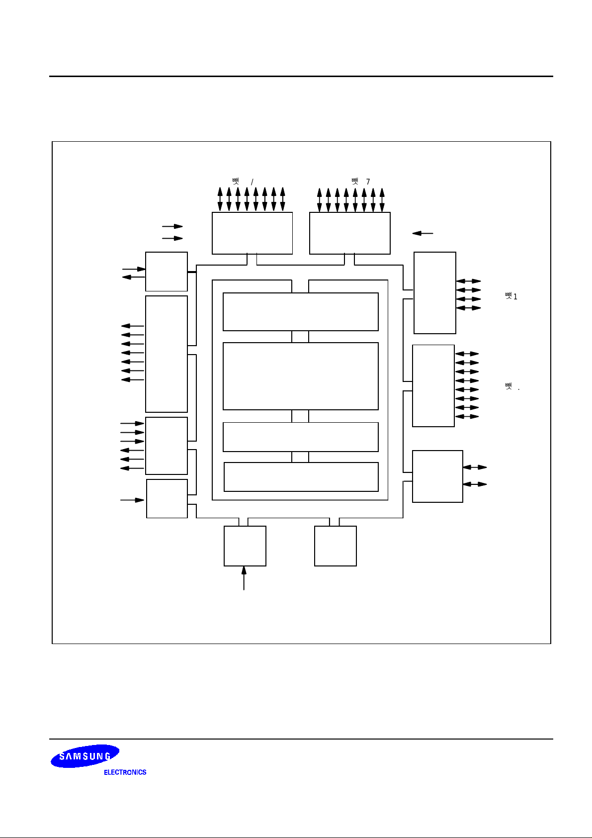
BLOCK DIAGRAM
X
X
OUT
PWM0
PWM1
•
•
•
PWM6
Vsync-I
Hsync-I
Csync-I
Vsync-O
Hsync-O
Clamp-O
T0CAP
IN
RESET
INT0-INT2
CESSOR
MAIN
OSC
8-BIT
PWM
(7-CH)
SYNC
PRO-
TIMER 0
P0.0k0.7/INT0-INT2
PORT 0
INTERNAL BUS
I/O PORT and INTERRUPT
SAM8 CPU
8/16-KBYTE MASK ROM
272-BYTE REGISTER FILE
CONTROL
P2.0k2.7
PORT 2
TEST
PORT 1
PORT3
DDC and
Multi master
IIC-bus
P1.0k1.3
P3.0k3.7
SCL
SDA
8-blt
Counter
(TIMER 1)
T1CK
Interval
timer
(TIMER 2)
Figure 1-2. Block Diagram
1-3
PRODUCT OVERVIEW KS88C6108/C6116/P6116 MICROCONTROLLERS
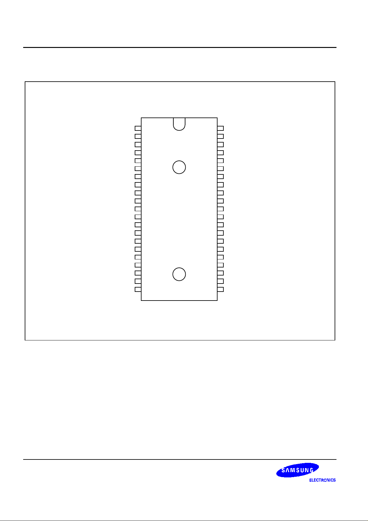
PIN ASSIGNMENTS
P3.1
P3.0
P0.0 / INT0
P0.1 / INT1
P0.2 / INT2
P0.3
P0.4 / T0CAP
P0.5 / T1CK
VDD
P0.6
P0.7
P1.0
P1.1
P1.2
P1.3
P2.0 / PWM0
P2.1 / PWM1
P2.2 / PWM2
P2.3 / PWM3
P2.4 / PWM4
P2.5 / PWM 5
1
2
3
4
5
6
7
8
9
10
11
12
13
14
15
16
17
18
19
20
21
KS88C6108/
KS88C6116
42-SDIP
(Top View)
42
41
40
39
38
37
36
35
34
33
32
31
30
29
28
27
26
25
24
23
22
P3.2
VSS2
P3.3
P3.4
P3.5
P3.6
P3.7
RESET
XOUT
XIN
VSS1
P2.7 / Csync-I
Hsync-I
Vsync-I (VCLK)
Clamp-O
Hsync-O
Vsync-O
SCL
SDA
TEST
P2.6 / PWM6
1-4
Figure 1-3. Pin Assignment Diagram (42-SDIP Package)
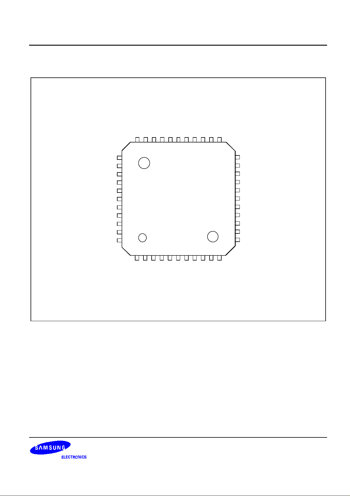
KS88C6108/C6116/P6116 M ICROCONTROLLERS PRODUCT OVERVIEW
PIN ASSIGNMENTS
P2.1 / PWM1
P2.2 / PWM2
P2.3 / PWM3
P2.4 / PWM4
P2.5 / PWM5
P2.6 / PWM6
(Cont.)
N.C.
TEST
SDA
SCL
Vsync-O
34
35
36
37
38
39
40
41
42
43
44
P2.0 / PWM0
P1.3
P1.2
33
32
31
P1.1
P1.0
P0.7
30
29
28
KS88C6108/
KS88C6116
44-QFP
(Top View)
P0.6
27
VDD
P0.5 / T1CK
26
25
P0.4 / T0CAP
P0.3
24
23
22
21
20
19
18
17
16
15
14
13
12
P0.2 / INT2
P0.1 / INT1
P0.0 / INT0
P3.0
P3.1
NC
P3.2
VSS2
P3.3
P3.4
P3.5
1
2
3
4
5
6
7
8
9
10
11
Hsync-O
Clamp-O
Vsync-I
Hsync-I
XIN
VSS1
P2.7 / Csync-I
XOUT
RESET
P3.7
P3.6
Figure 1-4. Pin Assignment Diagram (44-QFP Package)
1-5

PRODUCT OVERVIEW KS88C6108/C6116/P6116 MICROCONTROLLERS
PIN DESCRIPTIONS
Table 1-1. KS 88C6108/C6116/P6116 Pin Descriptions
Pin
Names
P0.0
P0.1
P0.2
P0.3
P0.4
P0.5
P0.6
P0.7
P1.0–P1.3 I/O General purpose, 8-bit I/O port. You can
Pin
Type
Pin
Descriptio n
I/O General-purpose, 8- bit I/O port. Share
functions include t hr ee ex ternal interrupt
inputs, I/O for timers 0 and 1. You can
selectively conf igur e por t 0 pins to input or
output mode.
Circuit
Type
SDIP Pin
Numbers
Functions
D-1 3
4
5
6
7
8
10
11
D-1 12–15 –
Shared
INT0
INT1
INT2
T0CAP
T1CK
selectively conf igur e por t 1 pins to input or
push-pull output mode.
P2.0
P2.1
P2.2
P2.3
P2.4
P2.5
P2.6
P2.7
P3.0–P3.7 I/O General-purpose, 8- bit I/O port. You can
I/O General purpose, 8-bit I/O port. You can
selectively conf igur e por t 2 pins to input or
output mode. T he por t 2 pin circuit are
designed to push-pull PWM output and
Csync signal input.
selectively conf igur e por t 3 pins to input or
D-1
D-1
D-1
D-1
E-1
E-1
E-1
D-1
16
17
18
19
20
21
22
31
E 2, 1, 42,
40–36
PWM0
PWM1
PWM2
PWM3
PWM4
PWM5
PWM6
Csync-I
output mode.
Hsync-I
Vsync-I
Clamp-O
Hsync-O
Vsync-O
SCL
SDA
V
DD
V
, V
SS1
XIN, X
OUT
SS2
I
The pins are sync proc es s or s ignal I/O and
I
IIC-bus clock and data I/O
O
O
O
I/O
I/O
A
A
A
A
A
G-3
G-3
30
29
28
27
26
25
24
– Power supply pins – 9
32, 41
– System clock input and output pins – 33, 34 –
RESET I System reset pin B 35 –
TEST I Fac tory test pin input
–23 –
0 V: normal operation
5 V: factory test mode
–
–
–
NOTE
: See ‘Pin Circuit Diagrams’ on next two pages for detailed inform ation on circuit types A, B, D-1, E, E-1, and G-3.
1-6

KS88C6108/C6116/P6116 M ICROCONTROLLERS PRODUCT OVERVIEW
PIN CIRCUITS
Vdd
Vss
Figure 1-5. Pin Circuit Type A
Data or
Other
function
Output
Disable
Vdd
280 K
Ω
Noise Filter
RESET
Figure 1-6. Pin Circuit Type B (
Vdd
Vss
RESET
)
Output
Digital Input
or TTL Input
Figure 1-7. Pin Circuit Type D-1
1-7
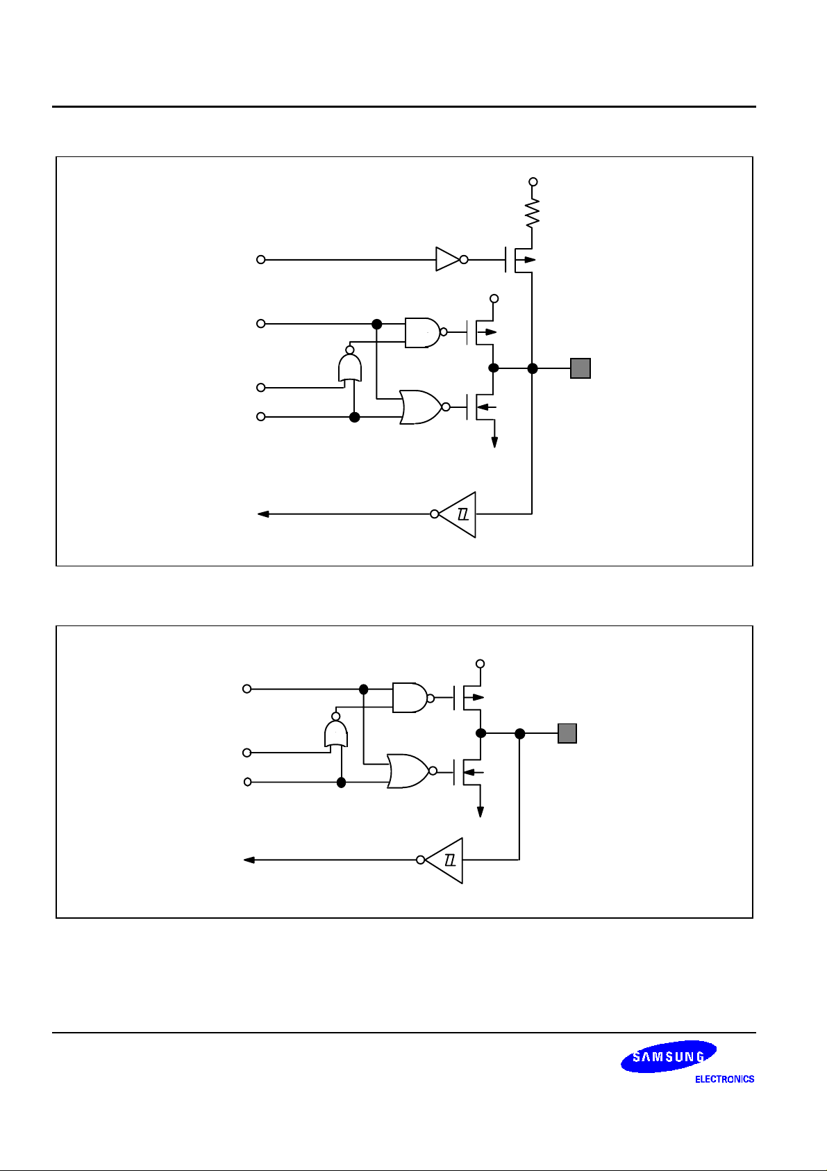
PRODUCT OVERVIEW KS88C6108/C6116/P6116 MICROCONTROLLERS
Vdd
Typical
47-K
Ω
Pull-up
enable
Vdd
Data
Output
Open drain
Output
Disable
Vss
Input
Data
Open drain
Output
Disable
Input
Figure 1-7. Pin Circuit Type E
Vdd
IN/OUT
Vss
1-8
Figure 1-8. Pin Circuit Type E-1

KS88C6108/C6116/P6116 M ICROCONTROLLERS PRODUCT OVERVIEW
Output
Data
Vss
Input
Figure 1-9. Pin Circuit Type G-3
1-9

PRODUCT OVERVIEW KS88C6108/C6116/P6116 MICROCONTROLLERS
NOTES
1-10

KS88C6108/C6116/P6116 MICROCONTROLLERS ELECTRICAL DATA
16
OVERVIEW
In this sect ion, KS
is arranged in the following order :
— Absolute maximum r atings
— D.C. electric al c har ac teristics
— I/O capacitance
— A.C. electr ic al c har ac teristics
— Oscillation charac teristics
— Oscillation st abiliz ation time
— Schmitt t r igger c har ac teristics
ELECTRICAL DATA
88C6108/C6116
electrical characteristics are pres ented in tables and graphs. T he information
16-1

ELECTRICAL DATA KS88C6108/C6116/P6116 MICROCONTROLLERS
Table 16-1. Absolute Maximum Ratings
= 25°C)
(T
A
Parameter Symbol Conditions Rating Unit
Supply voltage V
Input voltage V
Output volt age V
Output curr ent
I
DD
V
OH
I1
I2
O
Type C (n-channel, open- dr ain) – 0.3 to + 10 V
All port pins except V
All output pins – 0.3 to VDD + 0.3 V
One I/O pin active – 10 mA
– – 0.3 to + 7.0 V
I1
– 0.3 to VDD + 0.3
High
All I/O pins active – 60
Output curr ent
I
OL1
One I/O pin active + 30 mA
Low
I
OL2
I
OL3
Total pin current ex c ept port 3 + 100
Sync-processor I/O pins and IIC-bus
+ 150
clock and data pins
Operating
T
A
– – 40 to + 85
°
C
temperature
Storage
T
STG
– – 65 to + 150
°
C
temperature
Tabl e 16- 2. D.C. Electrical Characteristics
(T
A
= – 40
°
C to + 85°C, VDD = 4.5 V to 5.5 V)
Parameter Symbol Conditions Min Typ Max Unit
Input High
V
IH1
All input pins except V
IH2
and V
IH3
0.8 V
DD
–VDDV
voltage
Input Low
voltage
Output High
voltage
V
V
V
V
V
V
V
IH2
IH3
IL1
IL2
IL3
OH1
OH2
XIN, X
OUT
TTL input (HsyncI, VsyncI and CsyncI ) 2.0 V
All input pins except V
and V
IL3
XIN, X
OUT
IL2
V
– 0.5 V
DD
– – 0.2 V
DD
DD
0.4
TTL input (HsyncI, VsyncI and CsyncI ) 0.8
VDD= 4.5 V to 5.5 V
I
= – 8 mA Port 1 only
OH
VDD = 4.5 V to 5.5 V
I
= – 2 mA Port s 0, 2, ClampO, H
OH
– 1.0 – – V
V
DD
V
– 1.0
DD
DD
and VsyncO
V
OH3
VDD = 4.5 V to 5.5 V
I
= – 6 mA, Port 3
OH
V
DD
– 1.0
V
16-2

KS88C6108/C6116/P6116 MICROCONTROLLERS ELECTRICAL DATA
Tabl e 16- 2. D.C. Electrical Characteristics (Continued)
(T
A
= – 40
°
C to + 85°C, VDD = 4.5 V to 5.5 V)
Parameter Symbol Conditions Min Typ Max Unit
Output Low
voltage
V
OL1
V
OL2IOL
= 4.5 V to 5.5 V
V
DD
I
= 8 mA, port 1 only
OL
= 2 mA
––0.4V
0.4
Port 0, 2, Clam pO, HsyncO and
VsyncO
V
OL3IOL
= 6 mA
0.4
Port 3, SCL and SDA
Input High
leakage current
Input Low
leakage current
I
LIH1
I
LIH2
I
LIH3
I
LIL1
VIN = V
DD
All input pins except X
VIN = V
X
VIN = V
X
V
OUT
only
IN
= 0 V
IN
DD
only
DD
All input pins except X
––3µA
in, Xout
––20
2.5 6 20
––– 3µA
in, Xout
and RESET
Output High
leakage current
Output Low
I
LIL2
I
LIL3
I
LOHL
I
LOL
V
V
V
IN
IN
OUT
= 0 V; X
= 0 V; X
= V
DD
only – – – 20
OUT
only – 2.5 – 6 – 20
IN
––3µA
All output pins except port 1
V
= 0 V – – – 3 µA
OUT
leakage current
Pull-up resistor R
L1
V
= 0 V;
IN
V
= 4.5 V to 5.5 V
DD
20 47 80
Port 3
R
L2
V
= 0 V;
IN
V
= 4.5 V to 5.5 V
DD
150 280 480
RESET only
Supply current
(NOTE)
I
DD1
I
DD2
V
= 4.5 V to 5.5 V
DD
12 MHz CPU clock
Idle mode;
= 4.5 V to 5.5 V
V
DD
–1530mA
510
12 MHz CPU clock
I
DD3
Stop mode; V
= 5.0 V 1 10 µA
DD
kΩ
NOTE
: Supply current does not include drawn internal pull –up r esist or s and external loads of output .
16-3

ELECTRICAL DATA KS88C6108/C6116/P6116 MICROCONTROLLERS
RESET
RESET
Table 16-3. Data Retention Supply Voltage in Stop Mode
= – 40 °C to + 85 °C)
(T
A
Parameter Symbol Conditions Min Typ Max Unit
Data retention
V
DDDR
Stop mode 2 – 6 V
supply voltage
Data retention
I
DDDR
Stop mode, V
= 2.0 V – – 5 µA
DDDR
supply current
NOTES
:
1. During the oscillator stabilization wait time (t
2. Supply current does not include drawn through int ernal pul l –up r esist or s and external output current l oads.
≈≈
DATA RETENTION MODE
V
DD
EXECUTION OF
STOP INSTRUCTION
WAIT
NOTE
: t
is the same as 4096 × 32 × 1 / f
), all CPU operations m ust be stopped.
WAIT
OCCURS
STOP MODE
V
DDDR
OSC
.
OSCILLATION
STABILIZATION
t
WAIT
TIME
NORMAL
OPERATING
MODE
Figure 16-1. Stop Mode Release Timing When Initiated by a Reset
Table 16-4. Input/Output Capacitance
= –40°C to + 85°C, V
(T
A
DD
= 0 V)
Parameter Symbol Conditions Min Typ Max Unit
Input
capacitance
Output
C
C
IN
OUT
f = 1 MHz; unm eas ur ed pins
are connected to V
SS
– – 10 pF
capacitance
I/O capacitance C
16-4
IO

KS88C6108/C6116/P6116 MICROCONTROLLERS ELECTRICAL DATA
Tabl e 16- 5. A.C. Electrical Characteristics
= – 40°C to + 85°C, V
(T
A
= 4.5 V to 5.5V)
DD
Parameter Symbol Conditions Min Typ Max Unit
Noise Filter t
NF1H,
t
NF1L
t
NF2
P0.2–P0.0, T0CAP and
300 – – ns
T1CK (RC delay)
RESET only (RC delay) 800 – –
1 tCPU
t
NF1L
t
NF2
0.8 V
0.2 V
DD
DD
t
NF1H
NOTE
: The unit t
means one CPU clock period.
CPU
Figure 16-2. Input Timing Measurement Points for P0.0–P0.2, T0CAP and T1CK
16-5

ELECTRICAL DATA KS88C6108/C6116/P6116 MICROCONTROLLERS
Table 16-6. Oscillation Characteristics
= – 40°C + 85°C)
(T
A
Oscillator Clock Circuit Conditions Min Typ Max Unit
Main crystal or
ceramic
C1
C2
X
X
IN
OUT
V
= 4.5 V to 5.5 V 6 – 12 M Hz
DD
External clock
(main)
NOTE
: The maximum oscillator frequency is 12 MHz. If you use an oscillator frequency higher than 12 MHz, you cannot
select a non-divided CPU clock using CLKCON settings. That is, you must select one of the divide-by values.
X
X
IN
OUT
V
= 4.5 V to 5.5 V 6 – 12 M Hz
DD
Table 16-7. Oscillation Stabilization Time
= – 40°C + 85°C, VDD = 4.5 V to 5.5 V)
(T
A
Oscillator Test Condition Min Typ Max Unit
Crystal VDD = 4.5 V to 5.5 V – – 20 ms
Ceramic VDD = 4.5 V to 5.5V – – 10
External clock XIN input High and Low level width
(t
, tXL)
XH
NOTE
: Oscillation stabilization time is the time required for the CPU clock to return to its normal oscillation frequency after
a power-on occurs, or when Stop mode is released.
25 – 500 ns
16-6
f
1 /
OSC
t
t
XL
X
IN
XH
V
DD
=
0.5 V
0.4 V
Figure 16-3. Clock Timing Measurement Points for X
IN

KS88C6108/C6116/P6116 MICROCONTROLLERS ELECTRICAL DATA
V
out
V
DD
A : 0.2 V
DD
B : 0.4 V
C : 0.6 V
D : 0.8 V
V
SS
V
in
DD
DD
DD
AB CD
Figure 16-4. Schmitt Trigger Characteristics (Normal Po rt ; except TTL Input)
16-7

ELECTRICAL DATA KS88C6108/C6116/P6116 MICROCONTROLLERS
NOTES
16-8

KS88C6108/C6116/P6116 M ICROCONTROLLERS MECHANICAL DATA
17
OVERVIEW
The KS
a 44-QFP package ( S am s ung par t number 44-QFP- 1010B ) .
88C6116
0.2
=
14.00
microcontroller is av ailable in a 42- pin S DIP package (Samsung part number 42-SDIP-600) and
42 22
#1 21
MECHANICAL DATA
42-SDIP-600
15.24
0 ~ 15
°
(1.77)
0.50 =0.1
NOTE
39.10 =0.2
0.2
=
5.08MAX
0.3
1.00 =0.1
: Dimensions are in millimeters.
Figure 17-1. 42-Pin SDIP Package Mechanical Data (42- S DIP-600)
1.778
0.51MIN 3.50
=
3.30
+0.1
=
0.25
0.05
17-1

MECHANICAL DATA KS88C6108/C6116/P6116 M I CROCONTROLLERS
=
13.20
10.00
=
0.3
0.2
0~8°
0.15
+0.10
- 0.05
.20
=
0.80
0.3
0.2
=
13.20
=
10.00
44-QFP-1010B
0.10 MAX
#44
0.80
: Dimensions are in millimeters.
NOTE
Figure 17-2. 44-Pin QFP Package Mechanical Dat a ( 44- QFP-1010B)
#1
0.35
+0.10
- 0.05
(1.00)
0.05 MIN
=
2.05
2.30 MAX
0.10
17-2

KS88C6108/C6116/P6116 MICROCONTROLLERS KS88P6116 OTP
18
KS88P6116 OTP
OVERVIEW
The KS88P6116 single-chip CM OS microcontroller is the OTP (One Time Programmable) version of the
KS88C6108/C6116 microcontrollers. It has an on- c hip E P ROM instead of mask ed ROM. The EPRO M is
accessed by serial dat a format.
The KS88P6116 is fully c om patible with the KS88C6108/C6116, both in function and in pin configuration.
Because of its s im ple pr ogr am m ing r equir em ents, the KS88P6116 is ideal for use as an evaluation chip f or the
KS88C6108/C6116.
P3.1
P3.0
P0.0/INT0
P0.1/INT1
P0.2/INT1
P0.3
P0.4/T0CAP
P0.5/T1CK
/VDD
V
DD
P0.6
P0.7
/P1.0
SCLK
/P1.1
SDAT
P1.2
P1.3
P2.0/PWM0
P2.1/PWM1
P2.2/PWM2
P2.3/PWM3
P2.4/PWM4
P2.5/PWM5
1
2
3
4
5
6
7
8
9
10
11
12
13
14
15
16
17
18
19
20
21
KS88P6116
42-SDIP
(Top View)
42
41
40
39
38
37
36
35
34
33
32
31
30
29
28
27
26
25
24
23
22
P3.2
V
/
V
SS2
SS
P3.3
P3.4
P3.5
P3.6
P3.7
RESET/RESET
XOUT
XIN
V
/
V
SS1
SS
P2.7/Csync-1
Hsync-1
Hsync-1 (VCLK)
Clamp-O
Hsync-O
Vsync-O
SLC
SDA
TEST/
V
PP
P2.6/PWM6
NOTE:
The bolds indicate an OTP pin name.
Figure 18-1. KS88P6116 Pin Assignment s ( 42- S DIP Package)
18-1

KS88P6116 OTP KS88C6108/C6116/P6116 MICROCONTROLLERS
P2.1 / PWM1
P2.2 / PWM2
P2.3 / PWM3
P2.4 / PWM4
P2.5 / PWM5
N.C.
P2.6 / PWM6
/TEST
V
PP
SDA
SCL
Vsync-O
34
35
36
37
38
39
40
41
42
43
44
P2.0 / PWM0
P1.3
P1.2
33
32
31
1
2
3
SDAT
SCLK
P1.1 /
P1.0 /
P0.7
P0.6
30
29
28
27
KS88P6116
44-QFP
(Top View)
4
5
6
7
VDD
VDD /
26
8
P0.5 / T1CK
P0.4 / T0CAP
25
24
9
10
P0.3
11
23
22
21
20
19
18
17
16
15
14
13
12
P0.2 / INT2
P0.1 / INT1
P0.0 / INT0
P3.0
P3.1
NC
P3.2
VSS2 /
P3.3
P3.4
P3.5
VSS
Vsync-I
Hsync-O
Clamp-O
The bolds indicate an OTP pin name.
NOTE:
Hsync-I
/ VSS1
VSS
P2.7 / Csync-I
XIN
XOUT
P3.7
/ RESET
RESET
P3.6
Figure 18-2. KS88P6116 Pin Assignment s ( 44- QFP Package)
18-2

KS88C6108/C6116/P6116 MICROCONTROLLERS KS88P6116 OTP
Table 18-1.
Descriptions
of Pins Used to Read/Write the EPROM
Main Chip During Programming
Pin Name P in Name Pin No. I/O Function
P1.1 S DA T 13 (*30) I/O Serial DAT a P in ( Output when reading, I nput
when writing) Input & P us h- pull Output Port c an
be assigned
P1.0 SCLK 12 (*29) I Serial CLocK Pin (I nput Only Pin)
TEST VPP(TEST) 23 (*41) I EPROM Cell Writing Power Supply Pin
(Indicates O TP Mode Entering) W hen wr iting
12.5V is applied and when reading 5V is
applied.(Option)
RESET RESET 35 (*9) I Chip I nitialization
VDD / V
V
NOTE:
/
SS1
SS2
* means the 44-QFP OTP pin number .
VDD / V
V
SS
SS
/
9 / 32 / 41
(*26 / 6 / 15)
I Logic Power Supply Pin. VDD should be tied to
5V during programming.
Table 18-2. Comparison of KS88P6116 and KS88C6108/C6116 Features
Characteristic KS88P6116 KS88C6108/C6116
Program Memory 16 K byte EPROM 16 K byte mask ROM
Operating Voltage ( VDD) 4.5 V to 5.5 V 4.5 V to 5.5V
OTP Program m ing M ode VDD = 5 V, VPP(TEST)=12.5V
Pin Configuration 42SDIP, 44QFP 42SDIP, 44QFP
EPROM Program m ability User Program 1 time Programmed at t he factory
OPERATING MODE CHARACTERI S TICS
When 12.5 V is supplied t o the VPP(TEST) pin of the KS88P6116, t he E P ROM programming mode is ent er ed.
The operating mode (read, write, or read protection) is select ed ac c or ding to the input signals to the pins listed in
Table 16-3 below.
Table 18-3. Operating Mode Selection Criteria
V
DD
VPP
(TEST)
REG/
MEM
ADDRESS
(A15-A0)
R/
W
MODE
5 V 5 V 0 0000H 1 EPROM read
12.5 V 0 0000H 0 EPROM program
12.5 V 0 0000H 1 EPROM verify
12.5 V 1 0E3FH 0 EPROM read protection
NOTE
: "0" means Low level; "1" means High level.
18-3

KS88P6116 OTP KS88C6108/C6116/P6116 MICROCONTROLLERS
D.C. ELECTRICAL CHARACTERISTICS
Tabl e 18- 4. D.C. Electrical Characteristics
(T
= – 40
A
°
C to + 85 °C, VDD = 4.5 V to 5.5 V)
Parameter Symbol Conditions Min Typ Max Unit
Input High
leakage current
Input Low
leakage current
I
LIH1
I
LIH2
I
LIH3
I
LIL1
VIN = V
DD;
All input pins except X
VIN = V
X
VIN = V
X
V
OUT
only
IN
= 0 V;
IN
DD;
only
DD;
All input pins except X
––3µA
in, Xout
20
2.5 6 20
––– 3µA
in, Xout
and RESET
Output Hi gh
I
LIL2
I
LIL3
I
LOH1
V
IN
V
IN
V
OUT
= 0 V; X
= 0 V; X
= V
only – – – 20
OUT
only – 2.5 – 6 – 20
IN
DD
––3µA
leakage current
Output Low
I
LOL1
V
= 0 V – – – 3 µA
OUT
leakage current
Supply current I
DD1
Normal oper ating mode;
–1530mA
12 MHz CPU clock
I
DD2
IDLE mode;
510
12 MHz CPU clock
Data retention
I
DD3
VDDDR Stop mode 2 – 6 V
Stop mode; V
= 5.0 V – 1 10 µA
DD
supply v oltage
Data retention
IDDDR Stop mode; V DDDR = 2V – – 5 µ A
supply v oltage
18-4

KS88C6108/C6116/P6116 MICROCONTROLLERS KS88P6116 OTP
START
Address= First Location
VDD=5V, VPP=12.5V
x = 0
Program One 1ms Pulse
Increment X
FAIL
Device Failed
Verify Byte
YES
x = 10
NO
FAIL
NO
FAIL
Verify 1 Byte
Last Address
V
= VPP= 5 V
DD
Compare All Byte
PASS
Device Passed
Figure 18-3. OTP Programming Algorithm
Increment Address
18-5

KS88P6116 OTP KS88C6108/C6116/P6116 MICROCONTROLLERS
NOTE
18-6
 Loading...