

Page 1
120 / 128 CHANNEL TFT-LCD GATE DRIVER
KS0655
written permission of LCD Driver IC Team.
Prepared by: Jae il Byeon
November. 1999.
Ver. 0.1
Contents in this document are subject to change without notice. No part of this document may be reproduced
or transmitted in any form or by any means, electronic or mechanical, for any purpose, without the express
Page 2
KS0655 120 / 128 CHANNEL TFT-LCD GATE DRIVER
KS0655 Specification Revision History
Version Content Date
0.0 Original Aug.1999
0.1 The contents of page 9, 10, 13 and 14 have been modified Nov.1999
2
Page 3

120 / 128 CHANNEL TFT-LCD GATE DRIVER KS0655
CONTENTS
INTRODUCTION.................................................................................................... 4
FEATURES ............................................................................................................ 4
BLOCK DIAGRAM................................................................................................. 5
PIN ASSIGNMENTS............................................................................................. 6
PIN DESCRIPTIONS.............................................................................................. 7
ABSOLUTE MAXIMUM RATINGS........................................................................ 8
RECOMMENDED OPERATION RATINGS........................................................... 8
DC CHARACTERISTICS....................................................................................... 9
AC CHARACTERISTICS..................................................................................... 10
AC TIMING DIAGRAM......................................................................................... 11
OPERATION DESCRIPTION............................................................................... 12
OPERATION METHOD ........................................................................................................ 12
OUTPUT PIN........................................................................................................................ 13
VOLTAGE BIASING ............................................................................................................. 14
RECOMMENDED TIMING.................................................................................................... 15
3
Page 4

KS0655 120 / 128 CHANNEL TFT-LCD GATE DRIVER
INTRODUCTION
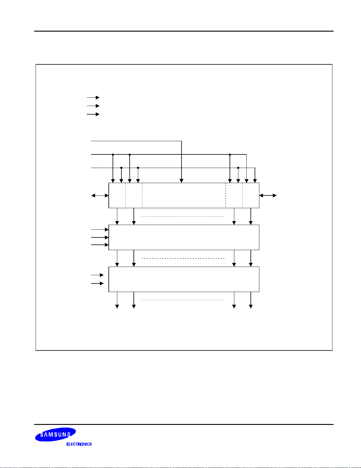
The KS0655 is a TFT-LCD gate driver having 120 / 128 outputs. It can drive TFT panel gate ON voltage up
to 40 V. It can operate within the logic voltage 3.0 to 5.5 V.
FEATURES
• 120 / 128 outputs
• Maximum TFT panel gate ON voltage = 40 V
• Bi-directional shift register
• Logic supply voltage = 3.0 to 5.5 V
• TCP
4
Page 5
120 / 128 CHANNEL TFT-LCD GATE DRIVER KS0655
BLOCK DIAGRAM
VDD
VLO
VSS
120/128
U/D
CPV
S / R
DI/O
001
S / R
002
128 Shift Register
S / R
127
S / R
128
DO/I
OE1
OE2
OE3
VGG
VOFF
Level Shifter
128 Ouput Buffer
G001 G002 G127 G128
Figure 1. Block Diagram
5
Page 6
KS0655 120 / 128 CHANNEL TFT-LCD GATE DRIVER
PIN ASSIGNMENTS
G001
G002
G003
G004
VOFF
VSS
DI/O
VLO
120/128
VDD
U/D
KS0655
(Top View)
CPV
OE3
OE2
OE1
DO/I
VGG
G125
G126
G127
G128
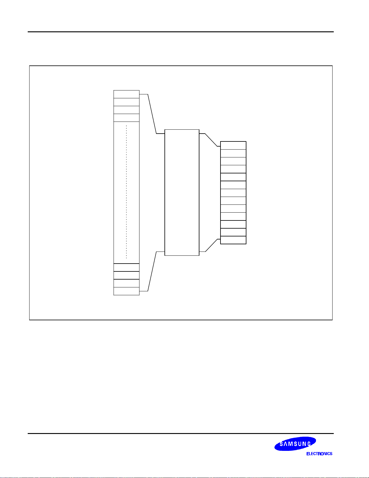
Figure 2. Pin Assignments
6
Page 7
120 / 128 CHANNEL TFT-LCD GATE DRIVER KS0655
PIN DESCRIPTIONS
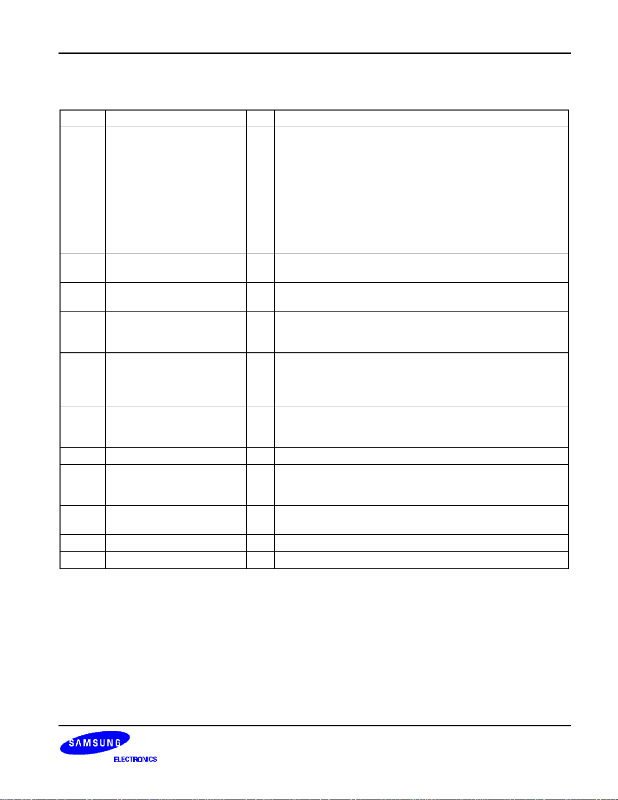
Symbol Pin Name I / O Description
When these inputs operate as the input, the start pulse data is
read at the rising edge of shift clock, CPV.
When these inputs operate as the output, the start pulse output
is the next chip’s start pulse input. The output pulse is
DI/O
DO/I
Start pulse input/output I / O
generated
at the falling edge of the 128th shift clock, CPV.
When U/D = H, the shift register does right shifting operation.
(Input = DI/O and output = DO/I)
When U/D = L, the shift register does left shifting operation.
(Input = DO/I and output = DI/O)
U/D Shift direction control input I
CPV Shift clock input I
120/128
OE1
OE2
OE3
G001
to
G128
VOFF Gate off voltage I This input is TFT-LCD gate off voltage.
VLO Logic input low voltage I
VSS Negative power supply I
VGG Driver positive power supply I The TFT gate ON voltage is VGG - VOFF.
VDD Logic positive power supply I This is the voltage source for internal logic operation.
Output selection input I
Output enable input I
Driver output O
When U/D = H, DI/O → G001 →……→ G128 → DO/I
When U/D = L, DO/I → G128 →……→ G001 → DI/O
The shift register operates in synchronization with the rising
edge of this input
This input selects the number of available outputs
When SEL = L, 128 output mode
When SEL = H, 120 output mode(G61 - G68 are disabled)
This input controls the state of the driver outputs.
When OE = H, the driver output is fixed to VOFF.
When OE = L, the driver output is VGG or VOFF corresponding
to the data.
The output signals change in synchronization with the rising
edge of shift clock input, CPV.
The amplitude of the driver output is VGG - VOFF.
This input operates as the reference to the level conversion of
the other input.
The other logic input range: VDD - VLO
This input is logic and driver ground.
Always, has negative potential.
7
Page 8

KS0655 120 / 128 CHANNEL TFT-LCD GATE DRIVER
ABSOLUTE MAXIMUM RATINGS (VSS = VOFF = 0 V)
Table 1. Absolute Maximum Ratings
Parameter Symbol Ratings Unit
Logic positive power supply VDD - 0.3 to 22.0 V
Driver positive power supply VGG - 0.3 to 45.0 V
Logic input low voltage VLO - 0.3 to VDD + 0.3 V
Input voltage VIN - 0.3 to VDD + 0.3 V
Operation temperature Top - 20 to 75
Storage temperature Tstg - 55 to 150
CAUTIONS
If the absolute maximum rating is exceeded momentarily, the quality of this product may be degraded.
It is desirable to use this product within the range of the absolute maximum ratings.
The power supplying order is as follows.
ON: VLO → VDD → VSS, VOFF → Control Input → VGG
OFF: VGG → Control Input → VSS, VOFF → VDD → VLO
°C
°C
RECOMMENDED OPERATION RATINGS (VLO = 0 V ≥≥ VSS = VOFF)
Table 2. Recommended Operation Ratings
Parameter Symbol Min. Typ. Max. Unit
Logic positive power supply VDD 3.0 - 5.5 V
Driver positive power supply VGG 6 - 40 V
Logic negative power supply VSS - 15 0 V
Driver negative power supply VOFF - 15 - 0 V
Power supply voltage VGG - VOFF 21 - 40 V
Operation frequency fCPV - - 100 kHz
Output load CL - - 500 pF
8
Page 9

120 / 128 CHANNEL TFT-LCD GATE DRIVER KS0655
DC CHARACTERISTICS (VLO = 0 V ≥≥ VSS = VOFF)
Table 3. DC Characteristics
(Ta = - 20 to 75 °°C, VGG - VOFF = 21 to 40 V, VLO - VSS = 15 to 0 V, VDD - VLO = 3.0 to 5.5 V)
Parameter Symbol Condition Min. Max. Unit Pin used
High input voltage VIH VLO + 0.9VX VDD V
Low input voltage VIL
High output voltage VOH
Low output voltage VOL
VX = VDD - VLO
IOH = - 40 µA
IOL = 40 µA
VSS
VDD - 0.4 VDD V
VSS VSS + 0.4 V
VLO +
0.1VX
VOUT = VGG - 0.5 V,
ROH
LCD driver output
ON resistance
ROL
VGG = 40 V,
VSS = VOFF = 0 V
VOUT = 0.5 V,
VGG = 40 V,
- 500 Ω
- 500 Ω
VSS = VOFF = 0 V
High output current IGG Without output load - 400
VDD - VSS = 3.3 V - 400
Low output current IDD
VDD - VSS = 19 V - 1000
Input leak current ILK - - 5 5
V
µA
µA
µA
µA
(1)
(2)
G001 to
G128
G001 to
G128
VGG
(1)
(3)
(1)
NOTES:
1. DI/O, DO/I, CPV, OE1, OE2, OE3, U/D, 120/128 used.
2. When U/D = H, DO/I used, and when U/D = L, DI/O used.
3. Input swing voltage = VDD to VDD - 3.3 V
9
Page 10

KS0655 120 / 128 CHANNEL TFT-LCD GATE DRIVER
AC CHARACTERISTICS (VLO = 0 V ≥≥ VSS = VOFF)
Table 4. AC Characteristics
(Ta = - 20 to 75 °°C, VGG - VOFF = 21 to 40 V, VLO - VSS = 15 to 0 V, VDD - VLO = 3.0 to 5.5 V)
Parameter Symbol Condition Min. Max. Unit
Clock period tCPV - 10 -
Clock pulse width tCPVH, tCPVL Duty = 50 % 4 -
Output enable input width twOE - 1 -
Data setup time tsDI - 700 -
Data hold time thDI - 700 Output delay time (1) tpdDO CL = 30 pF - 800
Output delay time (2) tpdG - 800
Output delay time (3) tpdOE
CL = 300 pF
- 800
µs
ns
10
Page 11

120 / 128 CHANNEL TFT-LCD GATE DRIVER KS0655
DI/O (U/D=H)
DO/I (U/D=L)
CPV
OE1~3
DO/I (U/D=H)
DI/O (U/D=L)
G1 (U/D=H)
G128 (U/D=L)
G128 (U/D=H)
G1 (U/D=L)
G2 to G127
50 %
50 %
AC TIMING DIAGRAM
tpdDO
50 %50 %
tCPV
tpdDO
tCPVH
50 %
50 %
50 %
tCPVL
tsDI thDI
50 % 50 %
twOE
50 %50 %
tpdOE
tpdOE
50 % 50 %
tpdG
Figure 3. AC Timing Diagram
50 %
11
Page 12
KS0655 120 / 128 CHANNEL TFT-LCD GATE DRIVER
OPERATION DESCRIPTION
OPERATION METHOD
The start pulse input, DI/O (when U/D is “H”) or DO/I (when U/D = “L”), is synchronized with the rising edge of
CPV and stored in the first shift register. While stored pulse is transferred to the next register at the next rising
edge of CPV, a new pulse is stored simultaneously. Output pin (G1 to G128) supplies VGG voltage or VOFF
voltage to the TFT-LCD panel depending on the pulse of the shift register.
The start pulse output, DO/I (when U/D is “H”) or DI/O (when U/D = “L”), is synchronized with the falling edge of
CPV and the pulse of the last register (G1 or G128) is transferred to the next IC. The voltage level of the start
pulse output is VDD with “H” data, VSS with “L” data
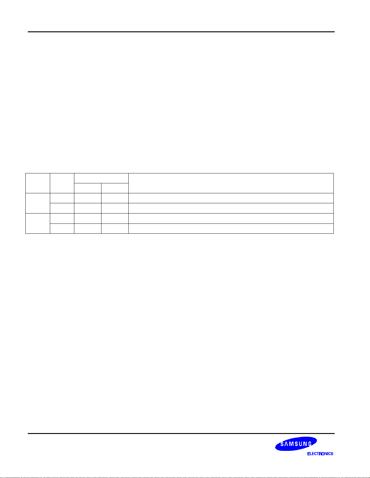
The relationship between U/D and shift data input / out pin is as follows:
Table 5. The Relationship between U/D and the Start Pulse Input / Output
Mode
128
output
120
output
U/D
state
“H” DI/O DO/I
“L” DO/I DI/O
“H” DI/O DO/I
“L” DO/I DI/O
Shift data
Input Output
Data transfer direction
G1 → G2 → G3 → G4 → G5 →……→ G128
G128 → G127 → G126 → G125 →……→ G1
G1 → G2 →……→ G60 → G69 →……→ G127 → G128
G128 → G127 →……→ G69 → G60 → ……→ G2 → G1
12
Page 13
120 / 128 CHANNEL TFT-LCD GATE DRIVER KS0655
OUTPUT PIN (G1 TO G128)
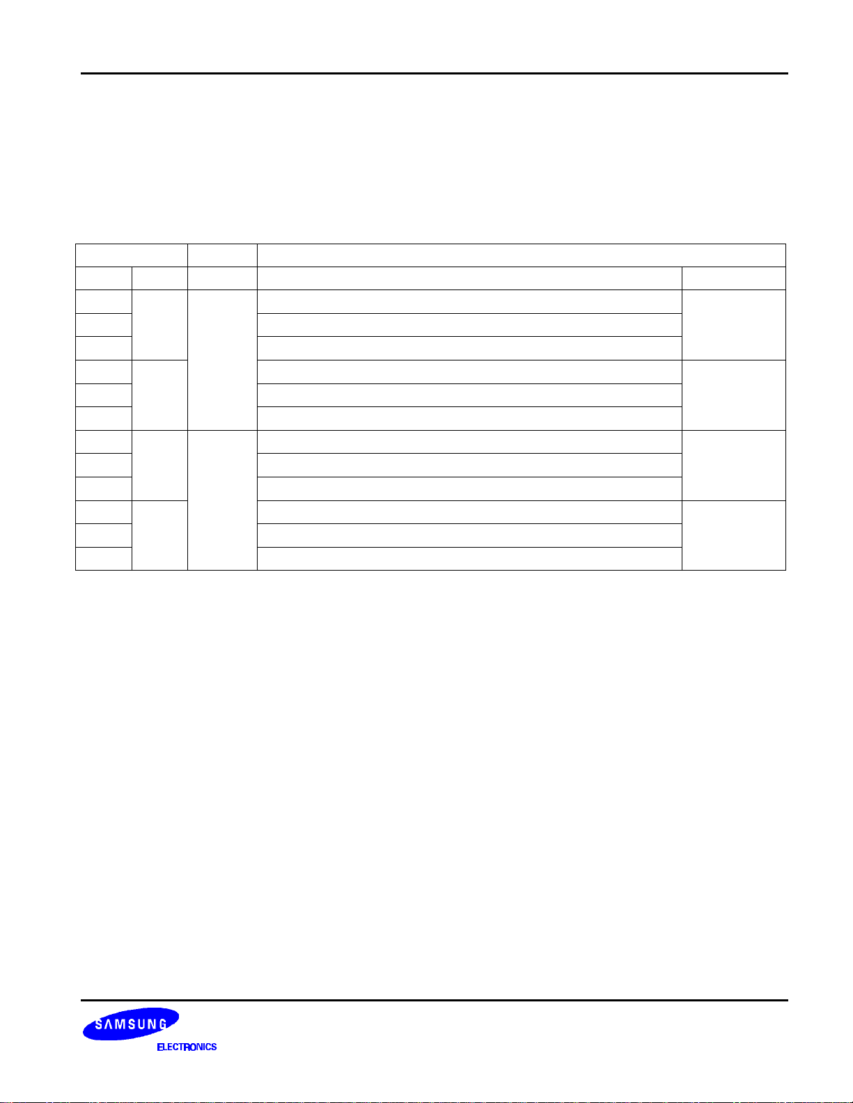
If the data of the shift register to an output drive pin is “H”, the voltage level of the output is VGG and if the data
is “L”, the level of the output is VOFF. But, when OE is “H”, the voltage level of the output is VOFF irrespective of
the data of the shift register.
Table 6. The Relationship between OE and the Output Level
Condition Mode Output pin control
Pin State 120/128 Control relationship Output level
OE1
OE2
OE3
OE1
OE2
OE3
OE1
OE2
OE3
OE1
OE2
OE3
“H”
120
Output
“L”
“H”
128
Output
“L”
G1, G4, G7,……, G55, G58, G69, G72,……, G123, G126
G2, G5, G8,……, G56, G59, G70, G73,……, G124, G127
G3, G6, G9,……, G57, G60, G71, G74,……, G125, G128
G1, G4, G7,……, G55, G58, G69, G72,……, G123, G126
G2, G5, G8,……, G56, G59, G70, G73,……, G124, G127
G3, G6, G9,……, G57, G60, G71, G74,……, G125, G128
G1, G4, G7,………………………………………, G124, G127
G2, G5, G8,………………………………………, G125, G128
G3, G6, G9,………………………………………, G126
G1, G4, G7,………………………………………, G124, G127
G2, G5, G8,………………………………………, G125, G128
G3, G6, G9,………………………………………, G126
VOFF
Normal output
(VGG / VOFF)
VOFF
Normal output
(VGG / VOFF)
13
Page 14
KS0655 120 / 128 CHANNEL TFT-LCD GATE DRIVER
VOLTAGE BIASING
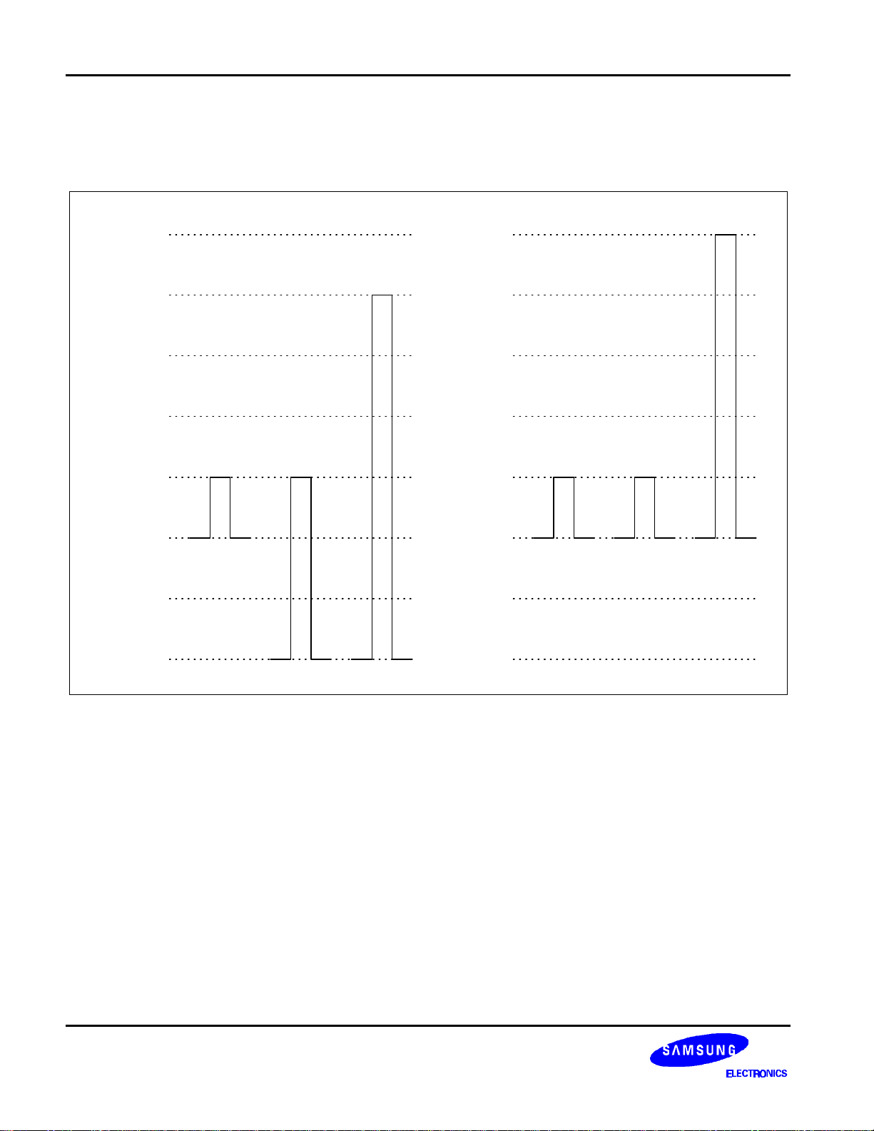
The driver negative power supply, VSS, can be any value between VLO and VLO - 15V.
G1 to G128
VGG (40 V)
G1 to G128
VGG (33 V)
VDD (3.3 V)
VLO (0 V)
VSS (-7 V)
= VOFF
Input
signal
Logic
Output
VDD (3.3 V)
VLO (0 V)
= VOFF = VSS
Figure 4. Example of Voltage Biasing
Input
signal
Logic
Output
14
Page 15

120 / 128 CHANNEL TFT-LCD GATE DRIVER KS0655
- 128 output mode
RECOMMENDED TIMING
When U/D = "H"
Input
DI/O
CPV
OE1
OE2
OE3
G1
G2
G3
G4
G128
Output
DO/I
When U/D = "L"
Input
DO/I
CPV
OE2
OE1
OE3
G128
G127
G126
G125
G1
VGG
VGG
VDD
VOFF
VSS
VOFF
Output
DI/O
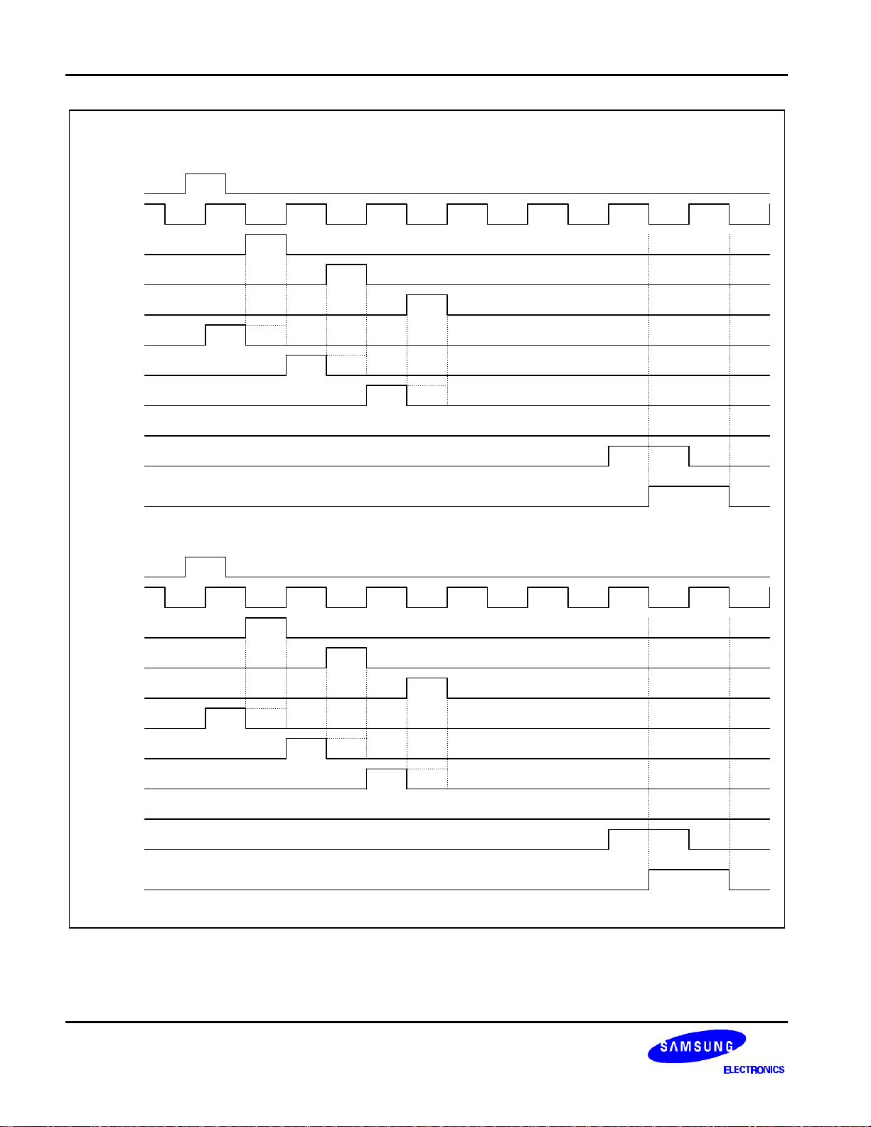
Figure 5. Recommended Timing
VDD
VSS
15
Page 16
KS0655 120 / 128 CHANNEL TFT-LCD GATE DRIVER
VOFF
- 120 output mode
When U/D = "H"
Input
DI/O
CPV
OE1
OE2
OE3
G1
G2
G3
G61 to
G68
G128
VGG
VOFF
VOFF
Output
DO/I
When U/D = "L"
Input
DO/I
CPV
OE3
OE2
OE1
G128
G127
G126
G68 to
G61
G1
Output
DI/O
VGG
VDD
VDD
VSS
VOFF
VSS
16
Figure 5. Recommended Timing (Continued)
Page 17

120 / 128 CHANNEL TFT-LCD GATE DRIVER KS0655
NOTES
17
 Loading...