

Page 1
查询KM416C4000C供应商
KM416C4000C, KM416C4100C CMOS DRAM
4M x 16bit CMOS Dynamic RAM with Fast Page Mode
DESCRIPTION
This is a family of 4,194,304 x 16 bit Fast Page Mode CMOS DRAMs. Fast Page Mode offers high speed random access of memory
cells within the same row. Refresh cycle(4K Ref. or 8K Ref.), access time ( -5 or -6) are optional features of this family. All of this family
have CAS-before-RAS refresh, RAS-only refresh and Hidden refresh capabilities. This 4Mx16 Fast Page Mode DRAM family is fabricated using Samsung′s advanced CMOS process to realize high band-width, low power consumption and high reliability.
FEATURES
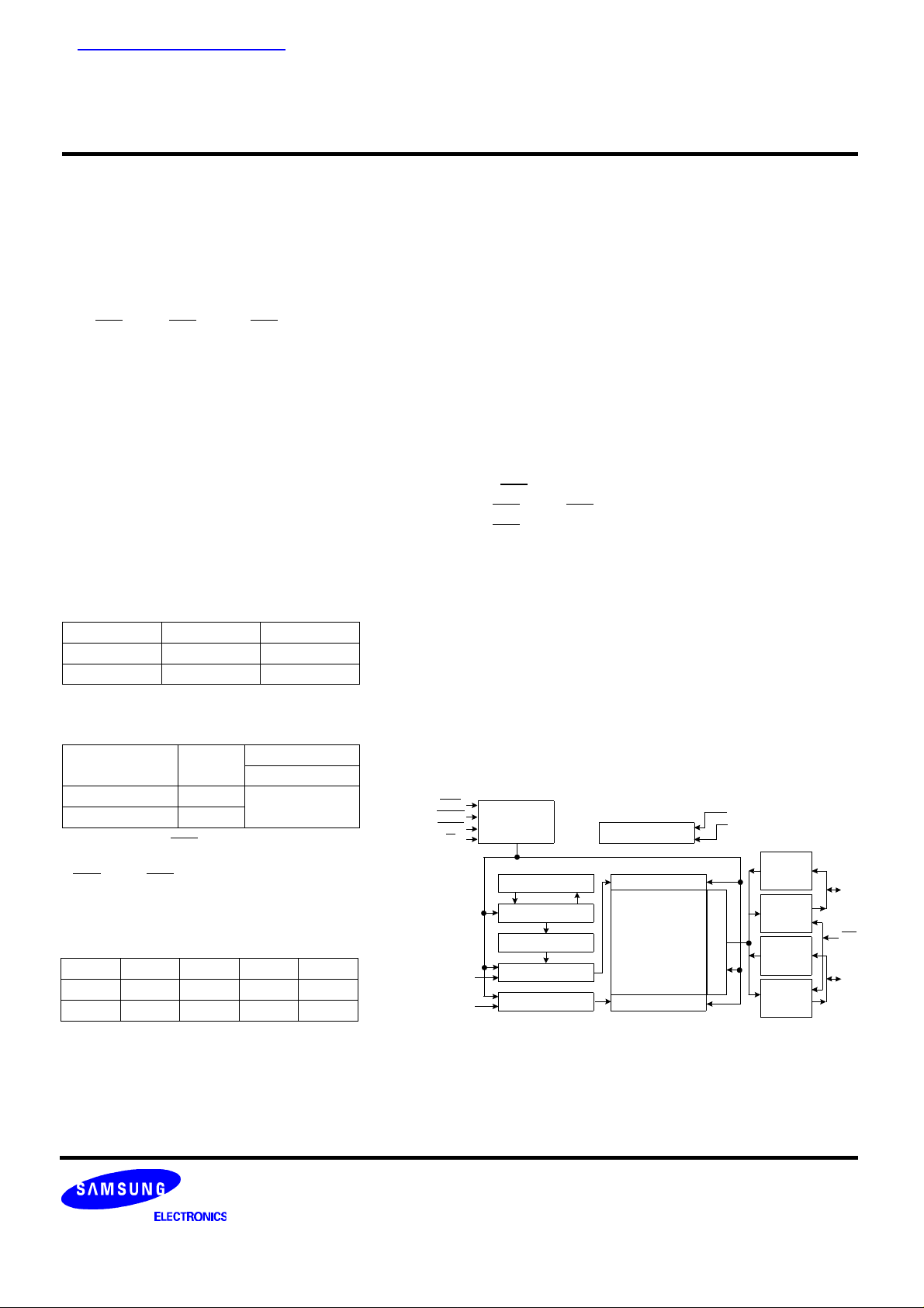
• Part Identification
- KM416C4000C(5.0V, 8K Ref.)
- KM416C4100C(5.0V, 4K Ref.)
• Active Power Dissipation
Speed 8K 4K
-5 495 660
-6 440 605
• Refresh Cycles
Part
NO.
KM416C4000C* 8K
KM416C4100C 4K
* Access mode & RAS only refresh mode
: 8K cycle/64ms
CAS-before-RAS & Hidden refresh mode
: 4K cycle/64ms
• Performance Range
Speed
tRAC tCAC tRC tPC
-5 50ns 13ns 90ns 35ns
-6 60ns 15ns 110ns 40ns
Refresh
cycle
Refresh time
Normal
64ms
Unit : mW
RAS
UCAS
LCAS
W
A0~A12
(A0~A11)*1
A0~A8
(A0~A9)*1
• Fast Page Mode operation
• 2CAS Byte/Word Read/Write operation
• CAS-before-RAS refresh capability
• RAS-only and Hidden refresh capability
• Fast parallel test mode capability
• TTL(5.0V) compatible inputs and outputs
• Early Write or output enable controlled write
• JEDEC Standard pinout
• Available in Plastic TSOP(II) package
• +5.0V±10% power supply
FUNCTIONAL BLOCK DIAGRAM
Control
Clocks
Refresh Timer
Refresh Control
Refresh Counter
Row Address Buffer
Col. Address Buffer
Note) *1 : 4K Refresh
VBB Generator
Row Decoder
Memory Array
4,194,304 x 16
Cells
Column Decoder
Vcc
Vss
Sense Amps & I/O
Lower
Data in
Buffer
Lower
Data out
Buffer
Upper
Data in
Buffer
Upper
Data out
Buffer
DQ0
to
DQ7
OE
DQ8
to
DQ15
SAMSUNG ELECTRONICS CO., LTD. reserves the right to
change products and specifications without notice.
Page 2
KM416C4000C, KM416C4100C CMOS DRAM
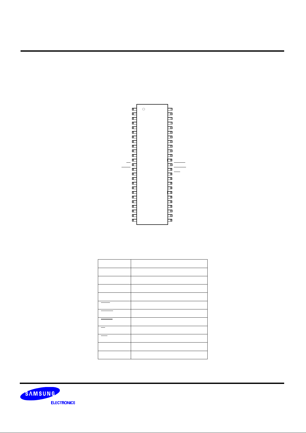
PIN CONFIGURATION (Top Views)
• KM416C40(1)00CS
VCC
DQ0
DQ1
DQ2
DQ3
VCC
DQ4
DQ5
DQ6
DQ7
N.C
VCC
RAS
N.C
N.C
N.C
N.C
VCC
*(N.C) : N.C for 4K Refresh Product
1
2
3
4
5
6
7
8
9
10
11
12
13
W
14
15
16
17
18
19
A0
20
A1
21
A2
22
A3
23
A4
24
A5
25
(400mil TSOP(II))
50
49
48
47
46
45
44
43
42
41
40
39
38
37
36
35
34
33
32
31
30
29
28
27
26
VSS
DQ15
DQ14
DQ13
DQ12
VSS
DQ11
DQ10
DQ9
DQ8
N.C
VSS
LCAS
UCAS
OE
N.C
N.C
A12(N.C)*
A11
A10
A9
A8
A7
A6
VSS
Pin Name Pin function
A0 - A12 Address Inputs(8K Product)
A0 - A11 Address Inputs(4K Product)
DQ0 - 15 Data In/Out
VSS Ground
RAS Row Address Strobe
UCAS Upper Column Address Strobe
LCAS Lower Column Address Strobe
W Read/Write Input
OE Data Output Enable
VCC Power(+5.0V)
N.C No Connection
Page 3
KM416C4000C, KM416C4100C CMOS DRAM
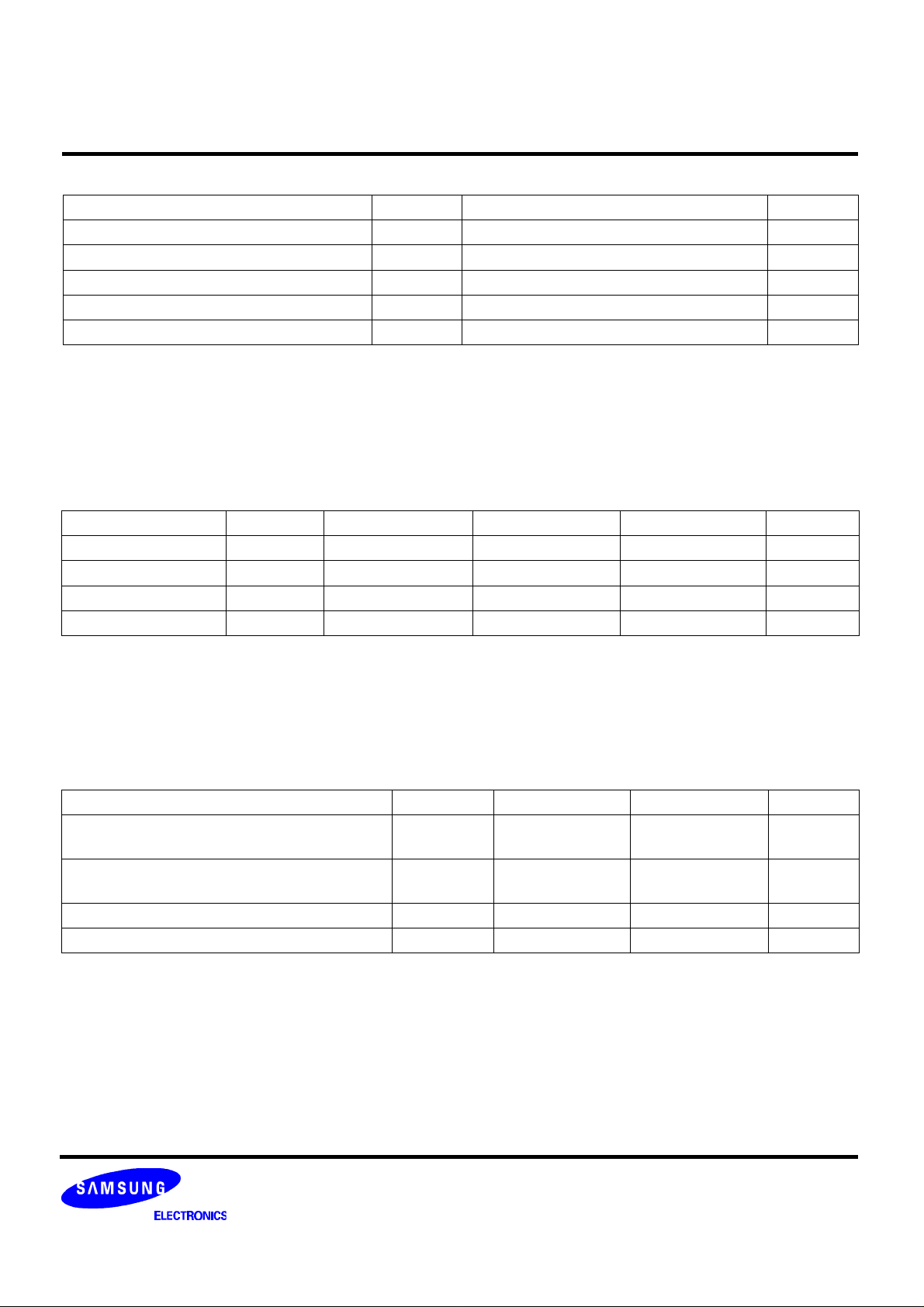
ABSOLUTE MAXIMUM RATINGS
Parameter Symbol Rating Units
Voltage on any pin relative to VSS VIN,VOUT -1.0 to +7.0 V
Voltage on VCC supply relative to VSS VCC -1.0 to +7.0 V
Storage Temperature Tstg -55 to +150 °C
Power Dissipation PD 1 W
Short Circuit Output Current IOS Address 50 mA
* Permanent device damage may occur if "ABSOLUTE MAXIMUM RATINGS" are exceeded. Functional operation should be restricted to
the conditions as detailed in the operational sections of this data sheet. Exposure to absolute maximum rating conditions for extended
periods may affect device reliability.
RECOMMENDED OPERATING CONDITIONS (Voltage referenced to Vss, TA= 0 to 70°C)
Parameter Symbol Min Typ Max Units
Supply Voltage VCC 4.5 5.0 5.5 V
Ground VSS 0 0 0 V
Input High Voltage VIH 2.6 Input Low Voltage VIL -1.0 - 0.7 V
*2
VCC+1.0
*1
V
*1 : VCC+2.0V at pulse width≤20ns which is measured at VCC
*2 : -2.0 at pulse width≤20ns which is measured at VSS
DC AND OPERATING CHARACTERISTICS (Recommended operating conditions unless otherwise noted.)
Parameter Symbol Min Max Units
Input Leakage Current (Any input 0≤VIN≤VCC+0.5V,
all other pins not under test=0 Volt)
Output Leakage Current
(Data out is disabled, 0V≤VOUT≤VCC)
Output High Voltage Level(IOH=-5mA) VOH 2.4 - V
Output Low Voltage Level(IOL=4.2mA) VOL - 0.4 V
II(L) -5 5 uA
IO(L) -5 5 uA
Page 4
KM416C4000C, KM416C4100C CMOS DRAM
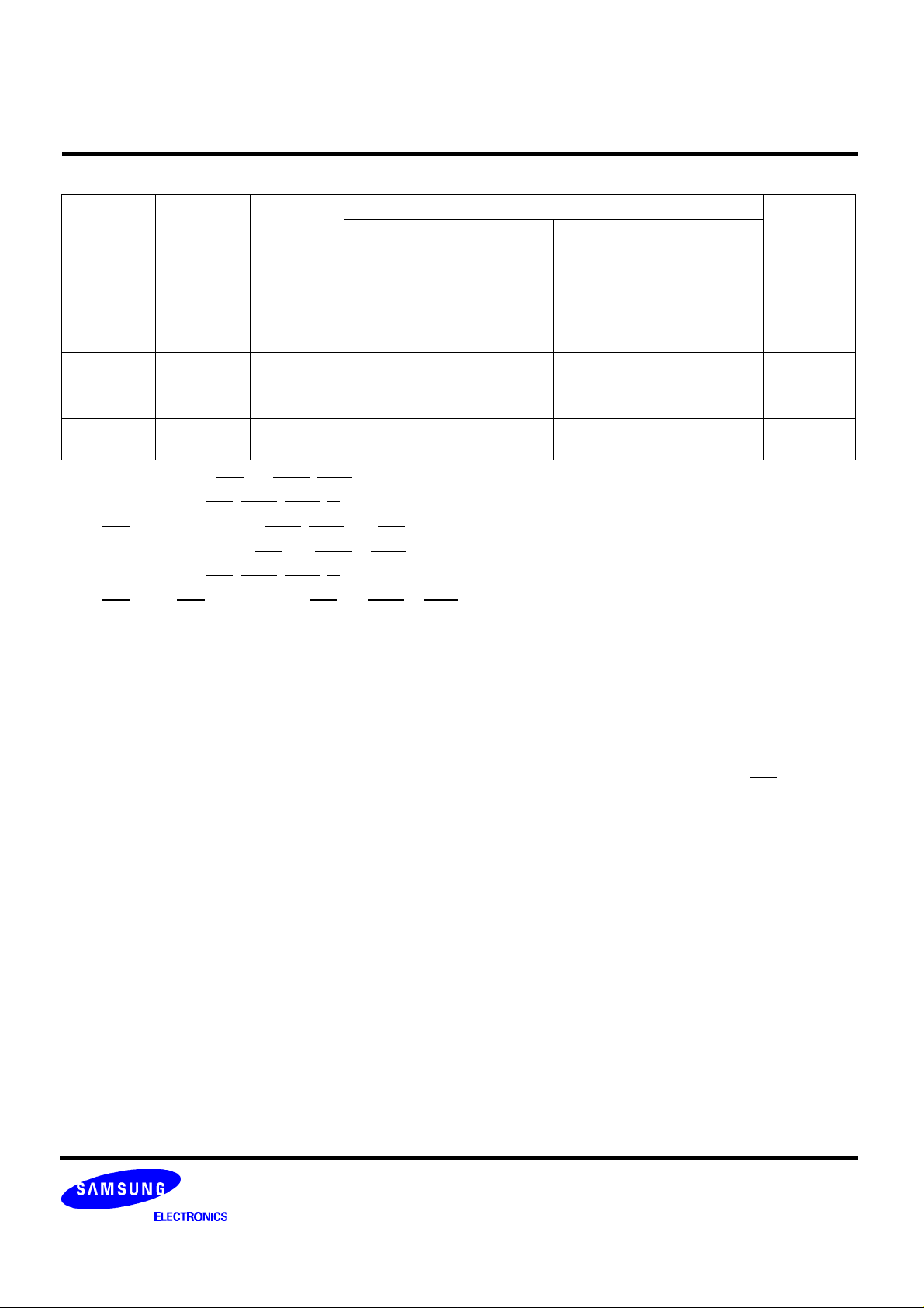
DC AND OPERATING CHARACTERISTICS (Continued)
Symbol Power Speed
ICC1 Don′t care
ICC2 Normal Don′t care 2 2 mA
ICC3 Don′t care
ICC4 Don′t care
ICC5 Normal Don′t care 1 1 mA
ICC6 Don′t care
ICC1* : Operating Current (RAS and UCAS, LCAS, Address cycling @tRC=min.)
ICC2 : Standby Current (RAS=UCAS=LCAS=W=VIH)
ICC3* : RAS-only Refresh Current (UCAS=LCAS=VIH, RAS, Address cycling @tRC=min.)
ICC4* : Fast Page Mode Current (RAS=VIL, UCAS or LCAS, Address cycling @tPC=min.)
ICC5 : Standby Current (RAS=UCAS=LCAS=W=VCC-0.2V)
ICC6* : CAS-Before-RAS Refresh Current (RAS and UCAS or LCAS cycling @tRC=min)
-5
-6
-5
-6
-5
-6
-5
-6
KM416C4000C KM416C4100C
90
80
90
80
60
50
120
110
Max
120
110
120
110
70
60
120
110
Units
mA
mA
mA
mA
mA
mA
mA
mA
*Note :
ICC1, ICC3, ICC4 and ICC6 are dependent on output loading and cycle rates. Specified values are obtained with the output open.
ICC is specified as an average current. In ICC1, ICC3 and ICC6, address can be changed maximum once while RAS=VIL. In ICC4,
address can be changed maximum once within one fast page mode cycle time, tPC.
Page 5
KM416C4000C, KM416C4100C CMOS DRAM
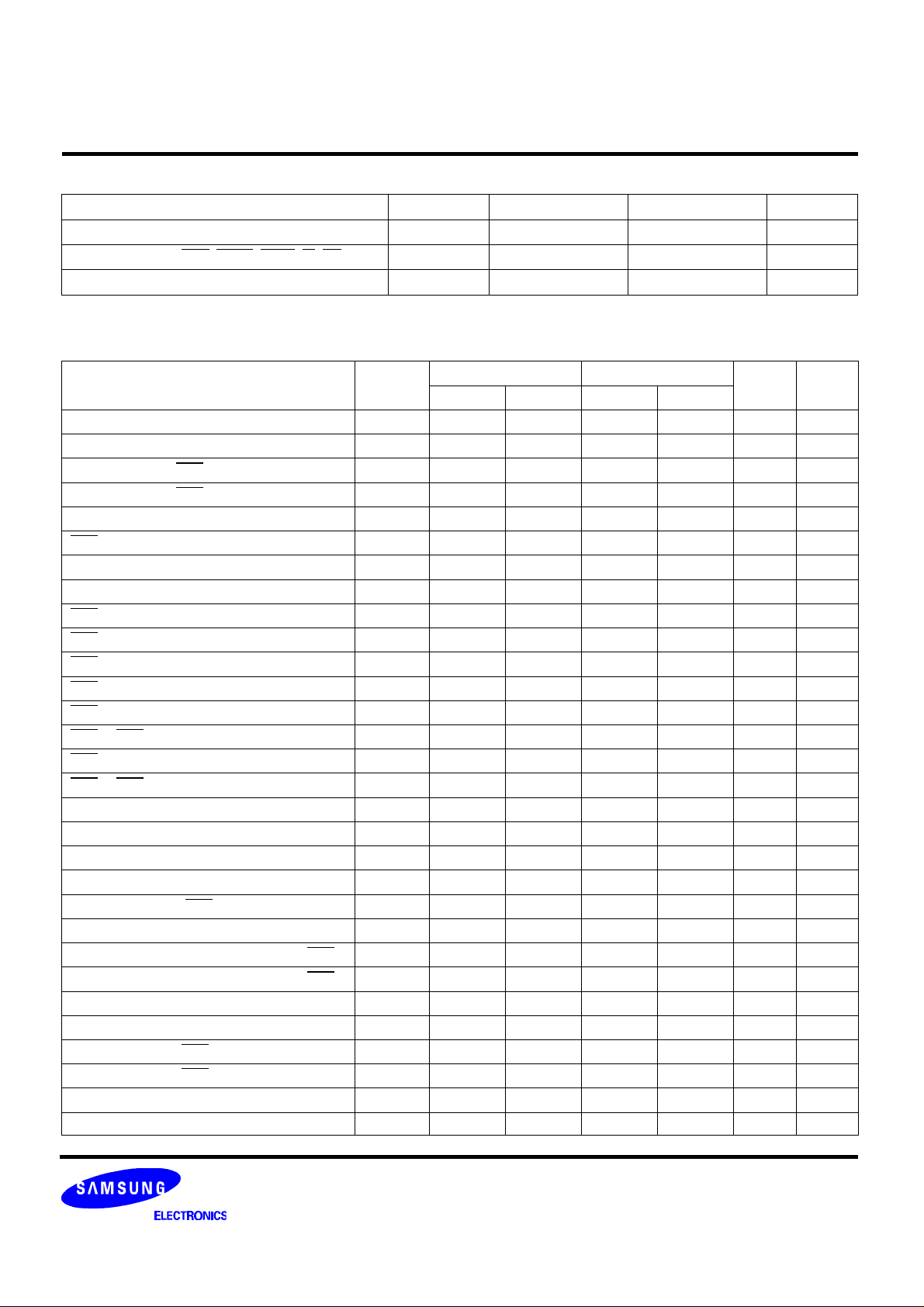
CAPACITANCE (TA=25°C, VCC=5.0V, f=1MHz)
Parameter Symbol Min Max Units
Input capacitance [A0 ~ A12] CIN1 - 5 pF
Input capacitance [RAS, UCAS, LCAS, W, OE] CIN2 - 7 pF
Output capacitance [DQ0 - DQ15] CDQ - 7 pF
AC CHARACTERISTICS (0°C≤TA≤70°C, See note 1,2)
Test condition : VCC=5.0V±10%, Vih/Vil=2.6/0.7V, Voh/Vol=2.4/0.6V
Parameter Symbol
Random read or write cycle time
Read-modify-write cycle time
Access time from RAS
Access time from CAS
Access time from column address
CAS to output in Low-Z
Output buffer turn-off delay
Transition time (rise and fall)
RAS precharge time
RAS pulse width
RAS hold time
CAS hold time
CAS pulse width
RAS to CAS delay time
RAS to column address delay time
CAS to RAS precharge time
Row address set-up time
Row address hold time
Column address set-up time
Column address hold time
Column address to RAS lead time
Read command set-up time
Read command hold time referenced to CAS
Read command hold time referenced to RAS
Write command hold time
Write command pulse width
Write command to RAS lead time
Write command to CAS lead time
Data set-up time
Data hold time
tRC
tRWC
tRAC
tCAC
tAA
tCLZ
tOFF
tT
tRP
tRAS
tRSH
tCSH
tCAS
tRCD
tRAD
tCRP
tASR
tRAH
tASC
tCAH
tRAL
tRCS
tRCH
tRRH
tWCH
tWP
tRWL
tCWL
tDS
tDH
-5 -6
Min Max Min Max
90 110
133 153 ns
50 60 ns 3,4,10
13 15 ns 3,4,5
25 30 ns 3,10
0 0 ns 3
0 13 0 13 ns 6
1 50 1 50 ns 2
30 40 ns
50 10K 60 10K ns
13 15 ns
50 60 ns
13 10K 15 10K ns
20 37 20 45 ns 4
15 25 15 30 ns 10
5 5 ns
0 0 ns
10 10 ns
0 0 ns 13
10 10 ns 13
25 30 ns
0 0 ns
0 0 ns 8
0 0 ns 8
10 10 ns
10 10 ns
15 15 ns
13 15 ns 16
0 0 ns 9,19
10 10 ns 9,19
Units Note
ns
Page 6
KM416C4000C, KM416C4100C CMOS DRAM
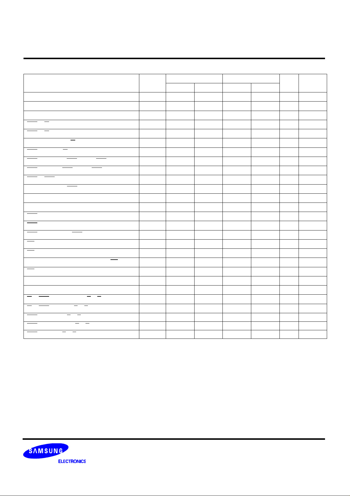
AC CHARACTERISTICS (Continued)
Parameter Symbol
Refresh period (4K, Normal)
Refresh period (8K, Normal)
Write command set-up time
CAS to W delay time
RAS to W delay time
Column address to W delay time
CAS precharge W delay time
CAS set-up time (CAS -before-RAS refresh)
CAS hold time (CAS -before-RAS refresh)
RAS to CAS precharge time
Access time from CAS precharge
Fast Page mode cycle time
Fast Page mode read-modify-write cycle time
CAS precharge time (Fast Page cycle)
RAS pulse width (Fast Page cycle)
RAS hold time from CAS precharge
OE access time
OE to data delay
Output buffer turn off delay time from OE
OE command hold time
Write command set-up time (Test mode in)
Write command hold time (Test mode in)
W to RAS precharge time (C-B-R refresh)
W to RAS hold time (C-B-R refresh)
RAS pulse width (C-B-R self refresh)
RAS precharge time (C-B-R self refresh)
CAS hold time (C-B-R self refresh)
tREF
tREF
tWCS
tCWD
tRWD
tAWD
tCPWD
tCSR
tCHR
tRPC
tCPA
tPC
tPRWC
tCP
tRASP
tRHCP
tOEA
tOED
tOEZ
tOEH
tWTS
tWTH
tWRP
tWRH
tRASS
tRPS
tCHS
-5 -6
Min Max Min Max
64 64 ms
64 64 ms
0 0 ns 7
36 38 ns 7,15
73 83 ns 7
48 53 ns 7
53 60 ns
5 5 ns 17
10 10 ns 18
5 5 ns
30 35 ns 3
35 40 ns
76 85 ns
10 10 ns 14
50 200K 60 200K ns
30 35 ns
13 15 ns
13 13 ns
0 13 0 13 ns 6
13 15 ns
10 10 ns 11
15 15 ns 11
10 10 ns
10 10 ns
100 100 us 20,21,22
90 110 ns 20,21,22
-50 -50 ns 20,21,22
Units Note
Page 7
KM416C4000C, KM416C4100C CMOS DRAM
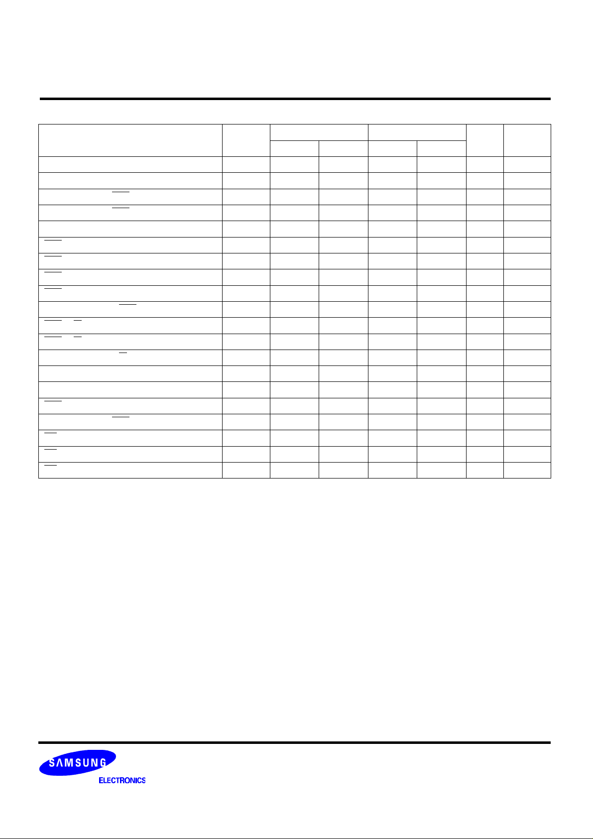
TEST MODE CYCLE
Parameter Symbol
Random read or write cycle time
Read-modify-write cycle time
Access time from RAS
Access time from CAS
Access time from column address
RAS pulse width
CAS pulse width
RAS hold time
CAS hold time
Column Address to RAS lead time
CAS to W delay time
RAS to W delay time
Column Address to W delay time
Fast Page mode cycle time
Fast Page mode read-modify-write cycle time
RAS pulse width (Fast Page cycle)
Access time from CAS precharge
OE access time
OE to data delay
OE command hold time
tRC
tRWC
tRAC
tCAC
tAA
tRAS
tCAS
tRSH
tCSH
tRAL
tCWD
tRWD
tAWD
tPC
tPRWC
tRASP
tCPA
tOEA
tOED
tOEH
( Note 11 )
-5 -6
Min Max Min Max
95 115 ns
138 160 ns
55 65 ns 3,4,10,12
18 20 ns 3,4,5,12
30 35 ns 3,10,12
55 10K 65 10K ns
18 10K 20 10K ns
18 20 ns
55 65 ns
30 35 ns
41 43 ns 7
78 88 ns 7
53 58 ns 7
40 45 ns
81 90 ns
55 200K 65 200K ns
35 40 ns 3
18 20 ns
18 18 ns
18 20 ns
Units Note
Page 8
KM416C4000C, KM416C4100C CMOS DRAM
NOTES
1.
An initial pause of 200us is required after power-up followed by any 8 RAS-only refresh or CAS-before-RAS refresh cycles
before proper device operation is achieved.
2.
VIH(min) and VIL(max) are reference levels for measuring timing of input signals. Transition times are measured between
VIH(min) and VIL(max) and are assumed to be 5ns for all inputs.
3.
Measured with a load equivalent to 2 TTL load and 100pF.
4.
Operation within the tRCD(max) limit insures that tRAC(max) can be met, tRCD(max) is specified as a reference point only.
If tRCD is greater than the specified tRCD(max) limit, then access time is controlled exclusively by tCAC.
5.
Assumes that tRCD≥tRCD(max).
6.
tOFF(min)and tOEZ(max) define the time at which the output achieves the open circuit condition and are not referenced Voh
or Vol.
tWCS, tRWD, tCWD and tAWD are non restrictive operating parameters. They are included in the data sheet as electrical char-
7.
acteristics only. If tWCS≥tWCS(min), the cycle is an early write cycle and the data output will remain high impedance for the
duration of the cycle. If tCWD≥tCWD(min), tRWD≥tRWD(min) and tAWD≥tAWD(min), then the cycle is a read-modify-write cycle
and the data output will contain the data read from the selected address. If neither of the above conditions is satisfied, the
condition of the data out is indeterminate.
Either tRCH or tRRH must be satisfied for a read cycle.
8.
These parameters are referenced to CAS falling edge in early write cycles and to W falling edge in read-modify-write cycles.
9.
Operation within the tRAD(max) limit insures that tRAC(max) can be met. tRAD(max) is specified as a reference point only.
10.
If tRAD is greater than the specified tRAD(max) limit, then access time is controlled by tAA.
These specifications are applied in the test mode.
11.
In test mode read cycle, the value of tRAC, tAA, tCAC is delayed by 2ns to 5ns for the specified values. These parameters
should be specified in test mode cycles by adding the above value to the specified value in this data sheet.
12.
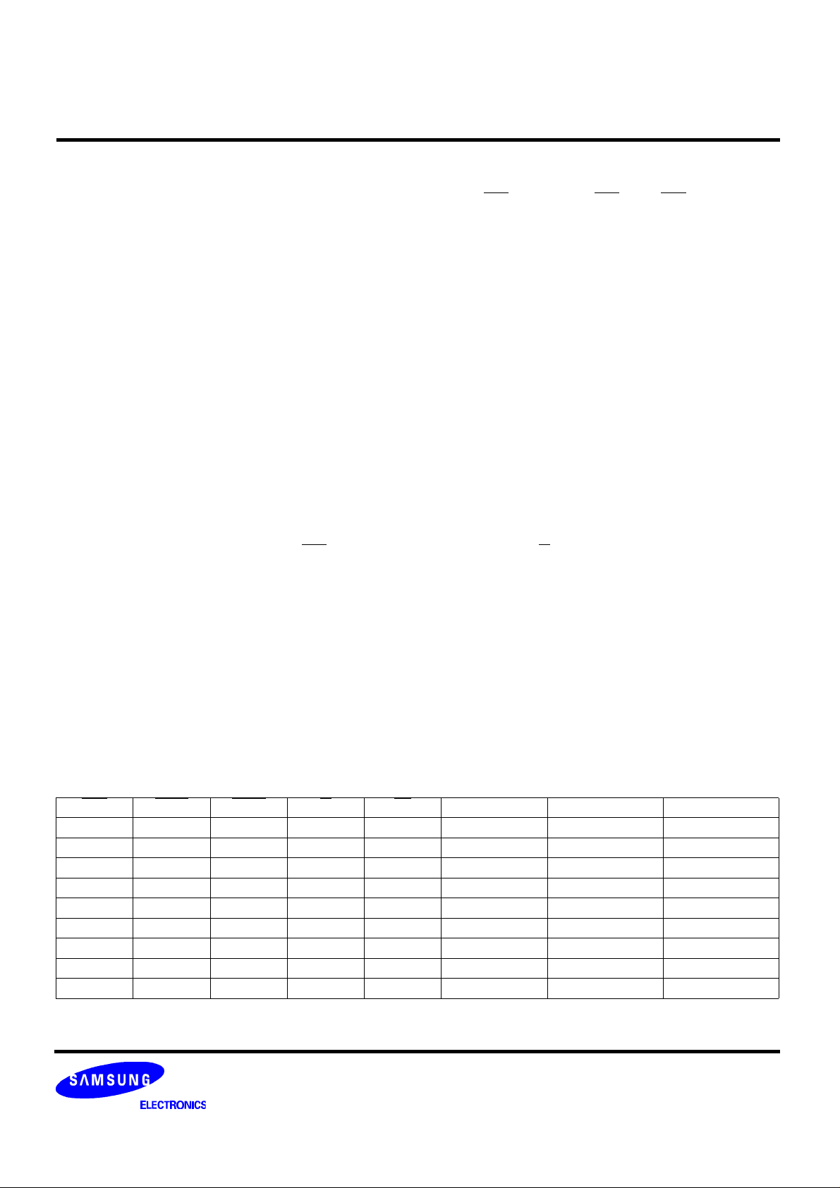
KM416C40(1)00C Truth Table
RAS LCAS UCAS W OE DQ0 - DQ7 DQ8-DQ15 STATE
H X X X X Hi-Z Hi-Z Standby
L H H X X Hi-Z Hi-Z Refresh
L L H H L DQ-OUT Hi-Z Byte Read
L H L H L Hi-Z DQ-OUT Byte Read
L L L H L DQ-OUT DQ-OUT Word Read
L L H L H DQ-IN - Byte Write
L H L L H - DQ-IN Byte Write
L L L L H DQ-IN DQ-IN Word Write
L L L H H Hi-Z Hi-Z -
Page 9
KM416C4000C, KM416C4100C CMOS DRAM
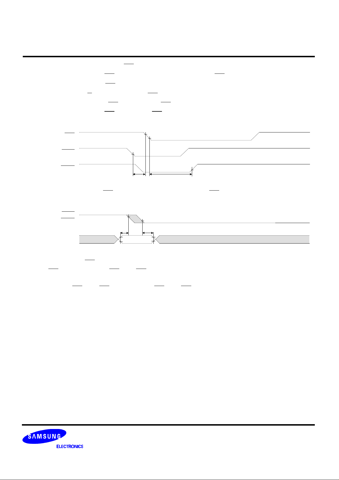
tASC, tCAH are referenced to the earlier CAS falling edge.
13.
14.
tCP is specified from the later CAS rising edge in the previous cycle to the earlier CAS falling edge in the next cycle.
15.
tCWD is referenced to the later CAS falling edge at word read-modify-write cycle.
16.
tCWL is specified from W falling edge to the earlier CAS rising edge.
17.
tCSR is referenced to the earlier CAS falling edge before RAS transition low.
18.
tCHR is referenced to the later CAS rising edge after RAS transition low.
RAS
LCAS
UCAS
tCSR tCHR
tDS is specified for the earlier CAS falling edge and tDH is specified by the later CAS falling edge.
19.
LCAS
UCAS
tDS tDH
DQ0 ~ DQ15
If tRASS≥100us, then RAS precharge time must use tRPS instead of tRP.
20.
21.
For RAS-only refresh and burst CAS-before-RAS refresh mode, 4096(4K/8K) cycles of burst refresh must be executed within
64ms before and after self refresh, in order to meet refresh specification.
For distributed CAS-before-RAS with 15.6us interval CAS-before-RAS refresh should be executed with in 15.6us immediately
22.
before and after self refresh in order to meet refresh specification.
Din
Page 10

KM416C4000C, KM416C4100C CMOS DRAM
WORD READ CYCLE
VIH -
RAS
VIL -
VIH -
UCAS
VIL -
VIH -
LCAS
VIL -
VIH -
A
VIL -
VIH -
W
VIL -
VIH -
OE
VIL -
DQ0 ~ DQ7
VOH -
VOL -
DQ8 ~ DQ15
VOH -
VOL -
tCRP
tCRP
tASR tRAH
ROW
ADDRESS
tRAD
OPEN
OPEN
tASC
tRCS
tCSH
tCSH
COLUMN
ADDRESS
tRAC
tRAC
tRAS
tCAH
tAA
tCLZ
tCLZ
tOEA
CAC
t
tCAC
tRC
tCAS
tCAS
tRAL
tRP
tRSHtRCD
tRSHtRCD
tCRP
tCRP
tRCH
tRRH
tOFF
tOEZ
DATA-OUT
tOFF
tOEZ
DATA-OUT
Don′t care
Undefined
Page 11
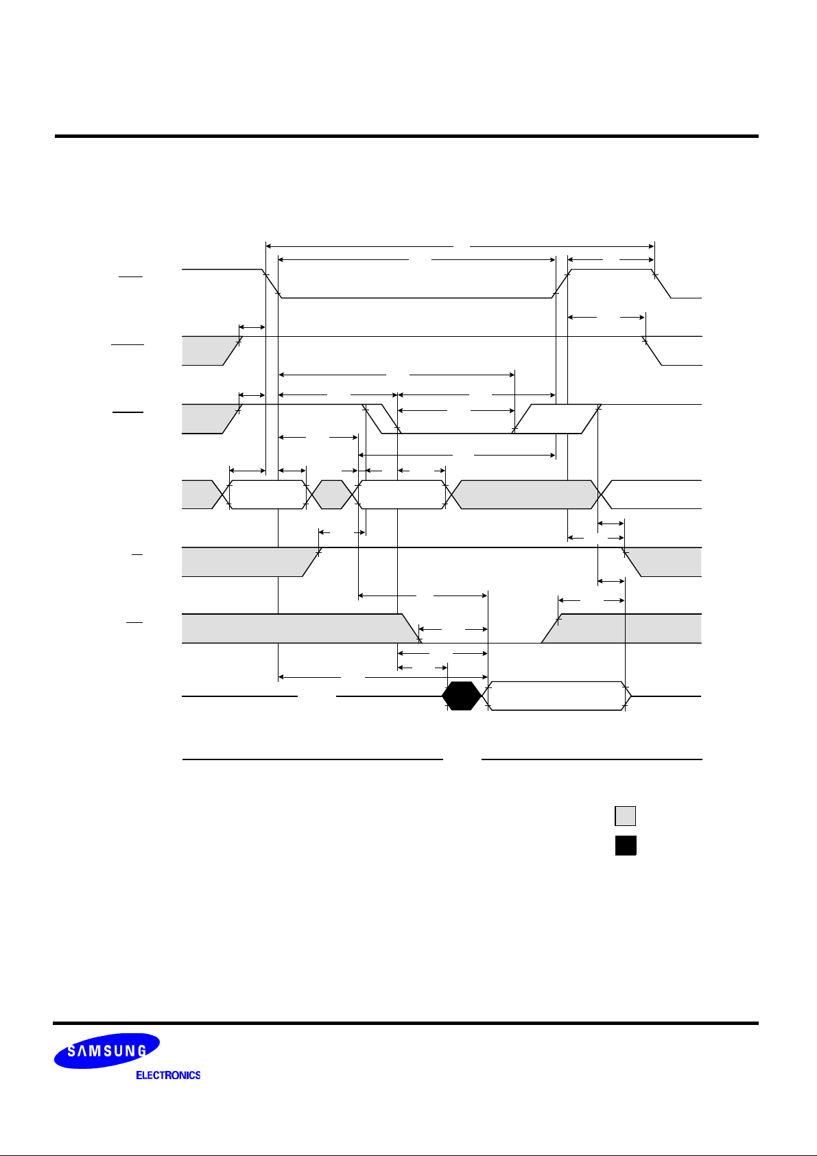
KM416C4000C, KM416C4100C CMOS DRAM
LOWER BYTE READ CYCLE
NOTE : DIN = OPEN
VIH -
RAS
VIL -
VIH -
UCAS
VIL -
VIH -
LCAS
VIL -
VIH -
A
VIL -
VIH -
W
VIL -
VIH -
OE
VIL -
DQ0 ~ DQ7
VOH -
VOL -
tCRP
tCRP
tASR tRAH
ROW
ADDRESS
tRAD
OPEN
tASC
tRCS
tRAC
tRAS
tCSH
tCAH
COLUMN
ADDRESS
tAA
tCLZ
tRC
tRP
tRPC
tRSHtRCD
tCAS
tRAL
tRCH
tRRH
tOFF
tOEZ
tOEA
tCAC
DATA-OUT
DQ8 ~ DQ15
VOH -
VOL -
OPEN
Don′t care
Undefined
Page 12
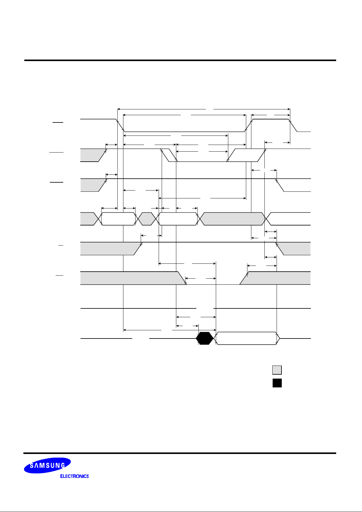
KM416C4000C, KM416C4100C CMOS DRAM
UPPER BYTE READ CYCLE
NOTE : DIN = OPEN
RAS
UCAS
LCAS
W
OE
A
VIH -
VIL -
VIH -
VIL -
VIH -
VIL -
VIH -
VIL -
VIH -
VIL -
VIH -
VIL -
tCRP
tCRP
tRAD
tASR tRAH tASC
ROW
ADDRESS
tRCS
tRAS
tCSH
tCAH
COLUMN
ADDRESS
tAA
tRSHtRCD
tCAS
tRAL
tOEA
tRC
tRP
tCRP
tRPC
tRCH
tRRH
tOFF
tOEZ
DQ0 ~ DQ7
VOH -
VOL -
DQ8 ~ DQ15
VOH -
VOL -
OPEN
tRAC
OPEN
tCAC
tCLZ
DATA-OUT
Don′t care
Undefined
Page 13
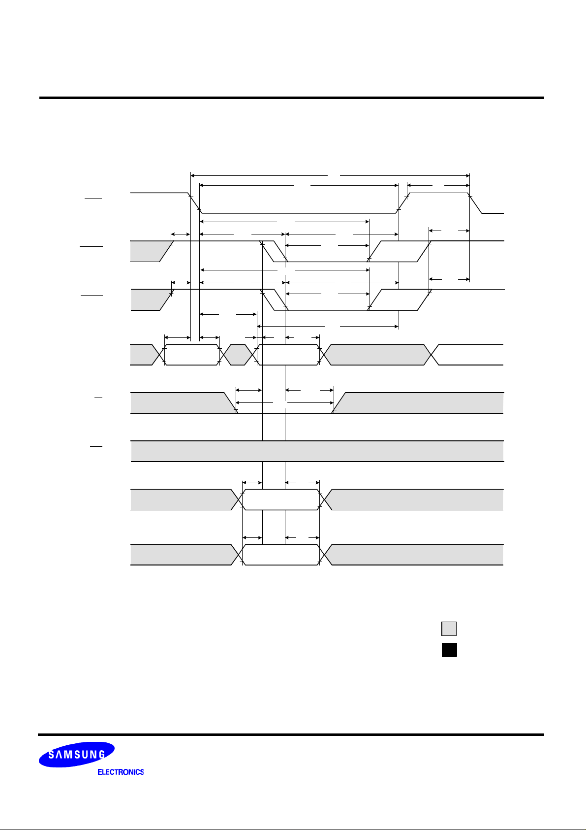
KM416C4000C, KM416C4100C CMOS DRAM
WORD WRITE CYCLE ( EARLY WRITE )
NOTE : DOUT = OPEN
RAS
UCAS
LCAS
W
OE
A
VIH -
VIL -
VIH -
VIL -
VIH -
VIL -
VIH -
VIL -
VIH -
VIL -
VIH -
VIL -
tCRP
tCRP
tRAD
tASR tRAH tASC
ROW
ADDRESS
tWCS
tRAS
tCSH
tCSH
tCAH
COLUMN
ADDRESS
tWP
tWCH
tRC
tCAS
tCAS
tRAL
tRP
tRSHtRCD
tRSHtRCD
tCRP
tCRP
DQ0 ~ DQ7
VIH -
VIL -
DQ8 ~ DQ15
VIH -
VIL -
tDS
tDS
tDH
DATA-IN
tDH
DATA-IN
Don′t care
Undefined
Page 14
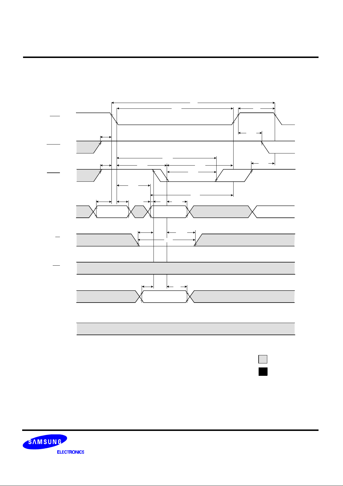
KM416C4000C, KM416C4100C CMOS DRAM
LOWER BYTE WRITE CYCLE ( EARLY WRITE )
NOTE : DOUT = OPEN
RAS
UCAS
LCAS
W
OE
A
VIH -
VIL -
VIH -
VIL -
VIH -
VIL -
VIH -
VIL -
VIH -
VIL -
VIH -
VIL -
tCRP
tCRP
tRAD
tASR tRAH tASC
ROW
ADDRESS
tWCS
tRAS
tCSH
tCAH
COLUMN
ADDRESS
tWP
tWCH
tRC
tCAS
tRAL
tRP
tRPC
tRSHtRCD
tCRP
DQ0 ~ DQ7
VIH -
VIL -
DQ8 ~ DQ15
VIH -
VIL -
tDS
tDH
DATA-IN
Don′t care
Undefined
Page 15
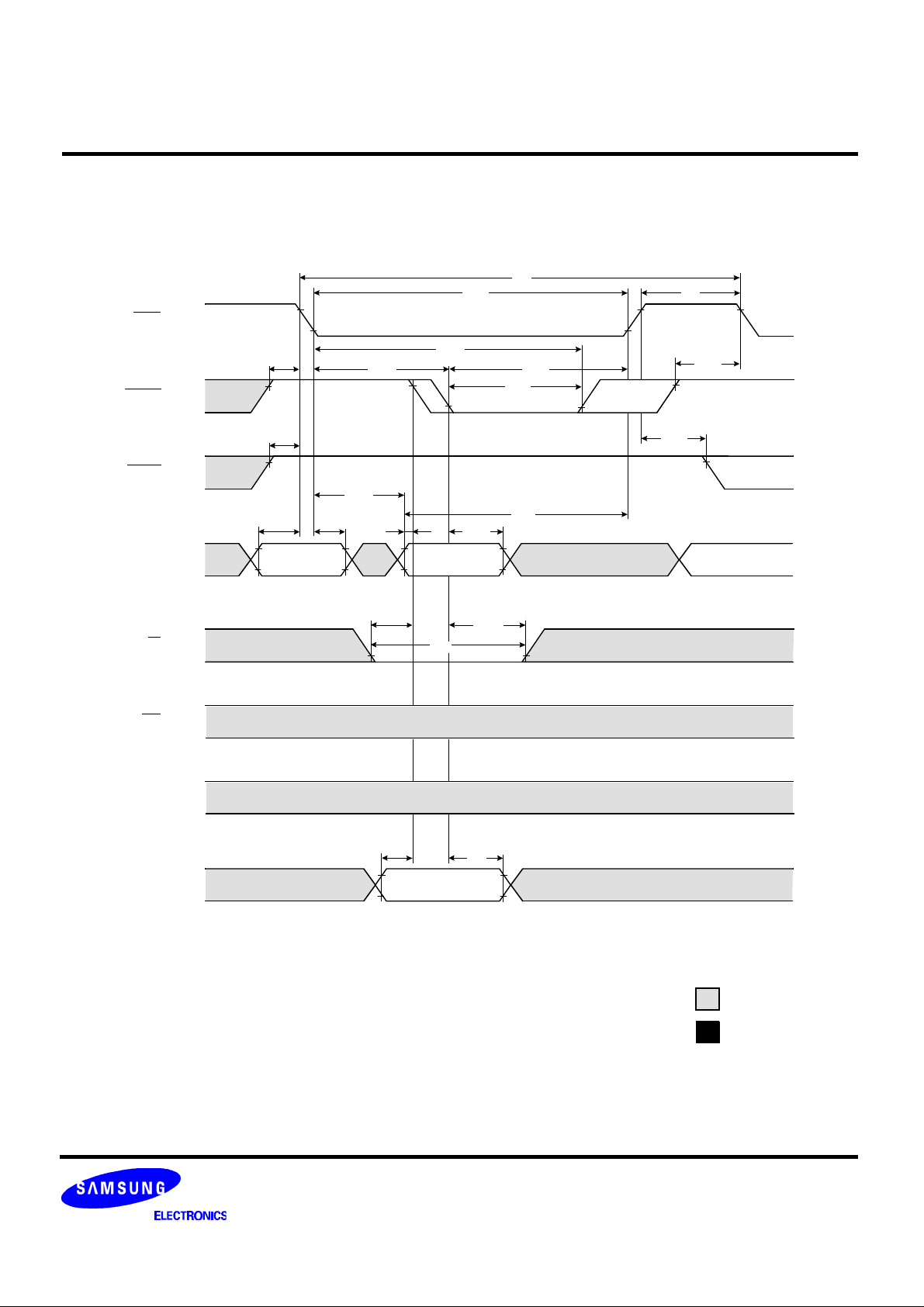
KM416C4000C, KM416C4100C CMOS DRAM
UPPER BYTE WRITE CYCLE ( EARLY WRITE )
NOTE : DOUT = OPEN
RAS
UCAS
LCAS
W
OE
A
VIH -
VIL -
VIH -
VIL -
VIH -
VIL -
VIH -
VIL -
VIH -
VIL -
VIH -
VIL -
tCRP
tCRP
tRAD
tASR tRAH tASC
ROW
ADDRESS
tWCS
tRAS
tCSH
tCAH
COLUMN
ADDRESS
tWP
tWCH
tRC
tCAS
tRAL
tRP
tRSHtRCD
tCRP
tRPC
DQ0 ~ DQ7
VIH -
VIL -
DQ8 ~ DQ15
VIH -
VIL -
tDS
tDH
DATA-IN
Don′t care
Undefined
Page 16
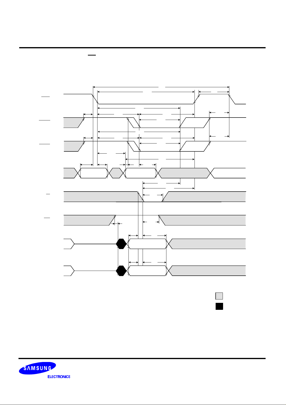
KM416C4000C, KM416C4100C CMOS DRAM
WORD WRITE CYCLE ( OE CONTROLLED WRITE )
NOTE : DOUT = OPEN
RAS
UCAS
LCAS
W
OE
A
VIH -
VIL -
VIH -
VIL -
VIH -
VIL -
VIH -
VIL -
VIH -
VIL -
VIH -
VIL -
tCRP
tCRP
tRAD
tASR tRAH tASC
ROW
ADDRESS
tOED
tRAS
tCSH
tCSH
tCAH
COLUMN
ADDRESS
tWP
tOEH
tRC
tCAS
tCAS
tRAL
tCWL
tRSHtRCD
tRSHtRCD
tRP
tCRP
tCRP
tRWL
DQ0 ~ DQ7
VIH -
VIL -
DQ8 ~ DQ15
VIH -
VIL -
tDS
tDS
tDH
DATA-IN
tDH
DATA-IN
Don′t care
Undefined
Page 17
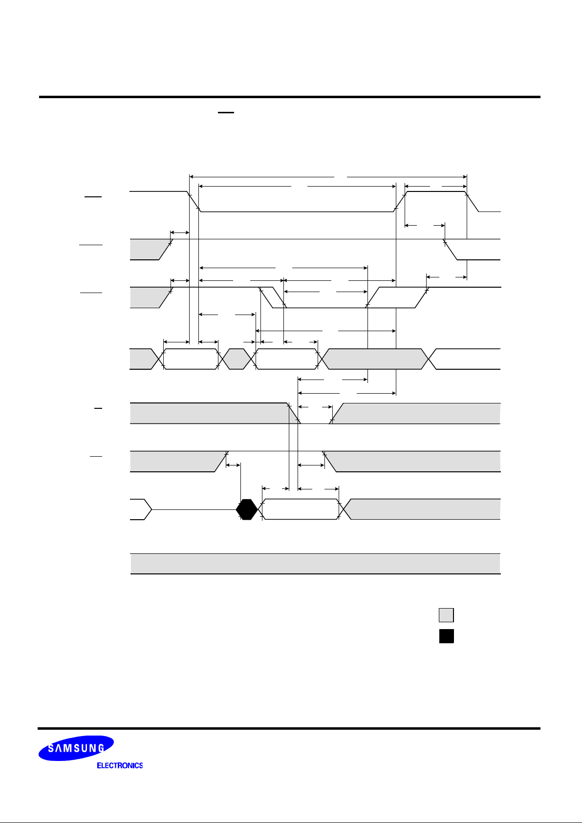
KM416C4000C, KM416C4100C CMOS DRAM
LOWER BYTE WRITE CYCLE ( OE CONTROLLED WRITE )
NOTE : DOUT = OPEN
RAS
UCAS
LCAS
W
OE
A
VIH -
VIL -
VIH -
VIL -
VIH -
VIL -
VIH -
VIL -
VIH -
VIL -
VIH -
VIL -
tRAS
tRC
tCRP tRPC
tCRP
tCSH
tRSHtRCD
tCAS
tRAD
tASR tRAH tASC
ROW
ADDRESS
tCAH
COLUMN
ADDRESS
tRAL
tCWL
tRWL
tWP
tOED
tOEH
tRP
tCRP
DQ0 ~ DQ7
VIH -
VIL -
DQ8 ~ DQ15
VIH -
VIL -
tDS
tDH
DATA-IN
Don′t care
Undefined
Page 18
KM416C4000C, KM416C4100C CMOS DRAM
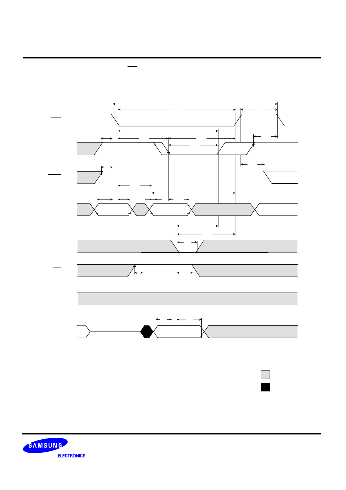
UPPER BYTE WRITE CYCLE ( OE CONTROLLED WRITE )
NOTE : DOUT = OPEN
RAS
UCAS
LCAS
W
OE
A
VIH -
VIL -
VIH -
VIL -
VIH -
VIL -
VIH -
VIL -
VIH -
VIL -
VIH -
VIL -
tCRP
tCRP
tRAD
tASR tRAH tASC
ROW
ADDRESS
tOED
tRAS
tCSH
tCAH
COLUMN
ADDRESS
tWP
tOEH
tRC
tCAS
tRAL
tCWL
tRSHtRCD
tRP
tCRP
tRPC
tRWL
DQ0 ~ DQ7
VIH -
VIL -
DQ8 ~ DQ15
VIH -
VIL -
tDS tDH
DATA-IN
Don′t care
Undefined
Page 19
KM416C4000C, KM416C4100C CMOS DRAM
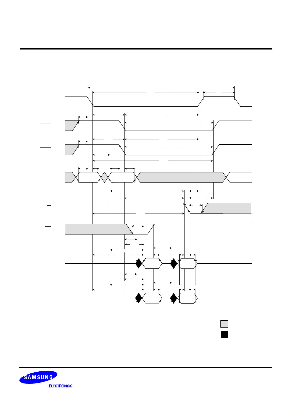
WORD READ - MODIFY - WRITE CYCLE
VIH -
RAS
VIL -
VIH -
UCAS
VIL -
VIH -
LCAS
VIL -
VIH -
A
VIL -
VIH -
W
VIL -
VIH -
OE
VIL -
DQ0 ~ DQ7
VI/OH -
VI/OL -
tCRP
tCRP
tRAD
tASR tRAH tASC tCAH
ROW
ADDR
COLUMN
ADDRESS
tCLZ
tAA
tRAC
tCLZ
tOEA
tCAC
tRWD
tRAS
tAWD
tCWD
VALID
DATA-OUT
tRWC
tRSHtRCD
tRSHtRCD
tCSH
tOED
tOEZ
tCAS
tCAS
tRWL
tDS tDH
VALID
DATA-IN
tRP
tCWL
tWP
DQ8 ~ DQ15
VI/OH -
VI/OL -
tRAC
tAA
tCAC
VALID
DATA-OUT
tOED
tOEZ
tDS
tDH
VALID
DATA-IN
Don′t care
Undefined
Page 20
KM416C4000C, KM416C4100C CMOS DRAM
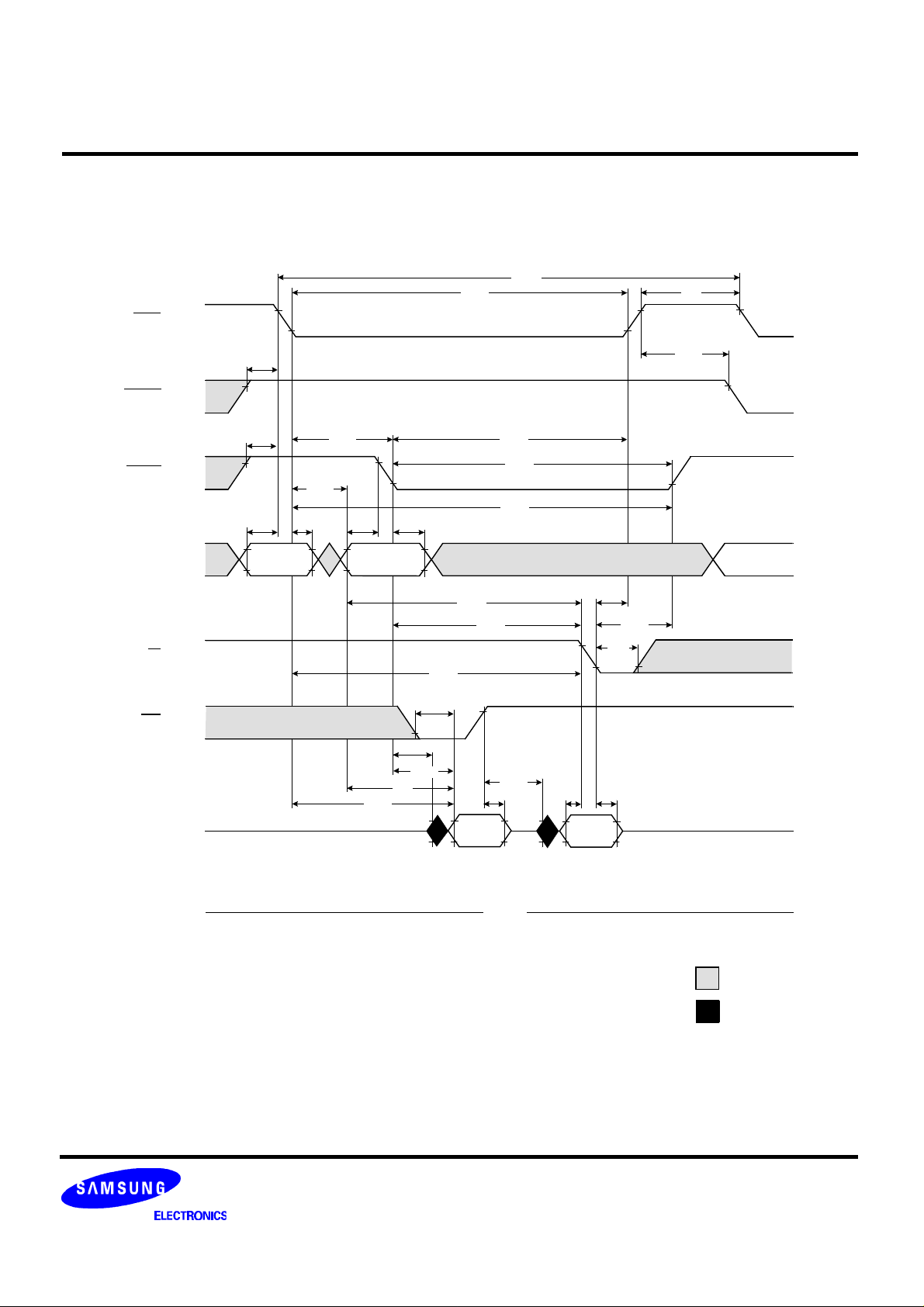
LOWER-BYTE READ - MODIFY - WRITE CYCLE
tRWC
RAS
UCAS
tRAS
VIH -
VIL -
tCRP
VIH -
VIL -
tRP
tRPC
VIH -
LCAS
VIL -
VIH -
A
VIL -
VIH -
W
VIL -
VIH -
OE
VIL -
DQ0 ~ DQ7
VI/OH -
VI/OL -
DQ8 ~ DQ15
VI/OH -
VI/OL -
tCRP
tRCD
tRAD
tASR tRAH tASC tCAH
ROW
ADDR
COLUMN
ADDRESS
tCLZ
tAA
tRAC
tOEA
tCAC
tRWD
tAWD
tCWD
VALID
DATA-OUT
OPEN
tRSH
tCAS
tCSH
tOED
tOEZ
tDS tDH
VALID
DATA-IN
tRWL
tCWL
tWP
Don′t care
Undefined
Page 21
KM416C4000C, KM416C4100C CMOS DRAM
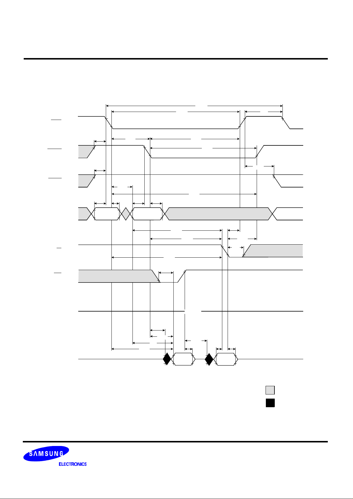
UPPER-BYTE READ - MODIFY - WRITE CYCLE
RAS
UCAS
LCAS
W
OE
A
VIH -
VIL -
VIH -
VIL -
VIH -
VIL -
VIH -
VIL -
VIH -
VIL -
VIH -
VIL -
tCRP
tCRP
tRAD
tASR tRAH tASC tCAH
ROW
ADDR
COLUMN
ADDRESS
tRWD
tOEA
tRAS
tAWD
tCWD
tRSHtRCD
tCSH
tRWC
tRP
tCAS
tRPC
tRWL
tCWL
tWP
DQ0 ~ DQ7
VI/OH -
VI/OL -
DQ8 ~ DQ15
VI/OH -
VI/OL -
tRAC
tAA
tCLZ
tCAC
OPEN
VALID
DATA-OUT
tOED
tOEZ
tDS
tDH
VALID
DATA-IN
Don′t care
Undefined
Page 22
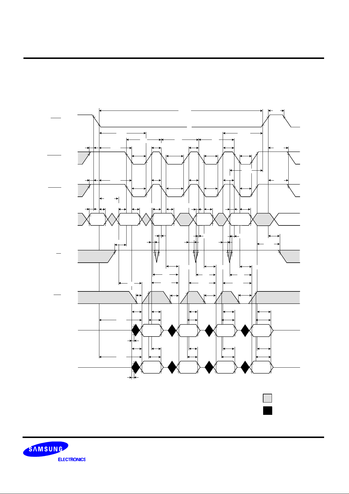
KM416C4000C, KM416C4100C CMOS DRAM
FAST PAGE MODE WORD READ CYCLE
RAS
UCAS
LCAS
W
OE
A
VIH -
VIL -
VIH -
VIL -
VIH -
VIL -
VIH -
VIL -
VIH -
VIL -
VIH -
VIL -
tRASP
¡ó
tCSH
tCRP
tRCD
tCRP
tRCD
tPC tPC tPC
tCP tCP tCP
tCAS tCAS tCAS tCAS
tCP tCP
tCAS tCAS tCAS tCAS
tRAD
tASR
tRAH tASC tCAH tCAH tCAH tASC tCAH
ROW
ADDR
COLUMN
ADDRESS
tASC
COLUMN
ADDRESS
tRCS
tRCS
tRCH tRCH
tASC
COLUMN
ADDR
tRCS
tRCH
tCAC
tAA
tCPA
tOEA
tAA
tOEA
tAA
tCPA
tOEA
tCAC
tCP
COLUMN
ADDRESS
tCPA
tRHCP
tRAL
tRCS
tAA
tOEA
tRP
tRPC
tRPC
tRRH
tRCH
tCAC
DQ0 ~ DQ7
VOH -
VOL -
DQ8 ~ DQ15
VOH -
VOL -
tCAC
tRAC
tCLZ
tCAC
tRAC
tCLZ
VALID
DATA-OUT
VALID
DATA-OUT
tOFF
tOEZ
tOFF
tOEZ
VALID
DATA-OUT
VALID
DATA-OUT
tOFF
tOEZ
tOFF
tOEZ
VALID
DATA-OUT
VALID
DATA-OUT
tOFF
tOEZ
tOFF
tOEZ
VALID
DATA-OUT
VALID
DATA-OUT
tOFF
tOEZ
tOFF
tOEZ
Don′t care
Undefined
Page 23
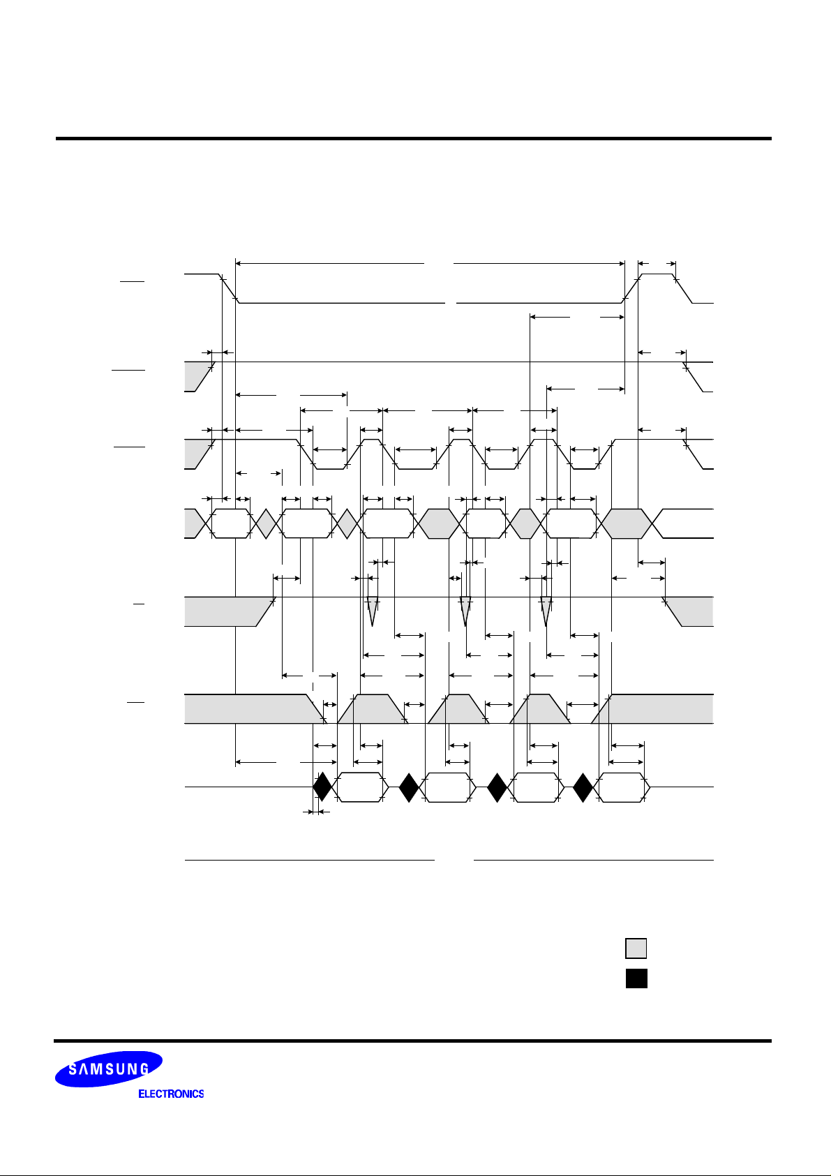
KM416C4000C, KM416C4100C CMOS DRAM
FAST PAGE MODE LOWER BYTE READ CYCLE
tRASP tRP
VIH -
RAS
UCAS
LCAS
A
VIL -
VIH -
VIL -
VIH -
VIL -
VIH -
VIL -
tCRP
tCSH
tCRP
tRCD
tPC tPC tPC
tCP tCP
tCAS tCAS tCAS tCAS
tRAD
tASR
tRAH tASC tCAH tASC tCAH tCAH tASC tCAH
ROW
ADDR
COLUMN
ADDRESS
COLUMN
ADDRESS
¡ó
tASC
COLUMN
ADDR
tCP
COLUMN
ADDRESS
tRHCP
tRPC
tRAL
tRPC
VIH -
W
VIL -
VIH -
OE
VIL -
DQ0 ~ DQ7
VOH -
VOL -
DQ8 ~ DQ15
OH -
V
VOL -
tRCS
tCAC
tRAC
tCLZ
tRCH tRCH
tAA
tAA
tCPA
tOEA
tOFF
tOEZ
VALID
DATA-OUT
tRCS
tOEA
tCAC
VALID
DATA-OUT
OPEN
tRCS
tAA
tCPA
tOEA
tOFF
tOEZ
tRCH
tCAC
VALID
DATA-OUT
tCPA
tOEA
tOFF
tOEZ
tRCS
tAA
tRCH
tCAC
VALID
DATA-OUT
tRRH
tOFF
tOEZ
Don′t care
Undefined
Page 24
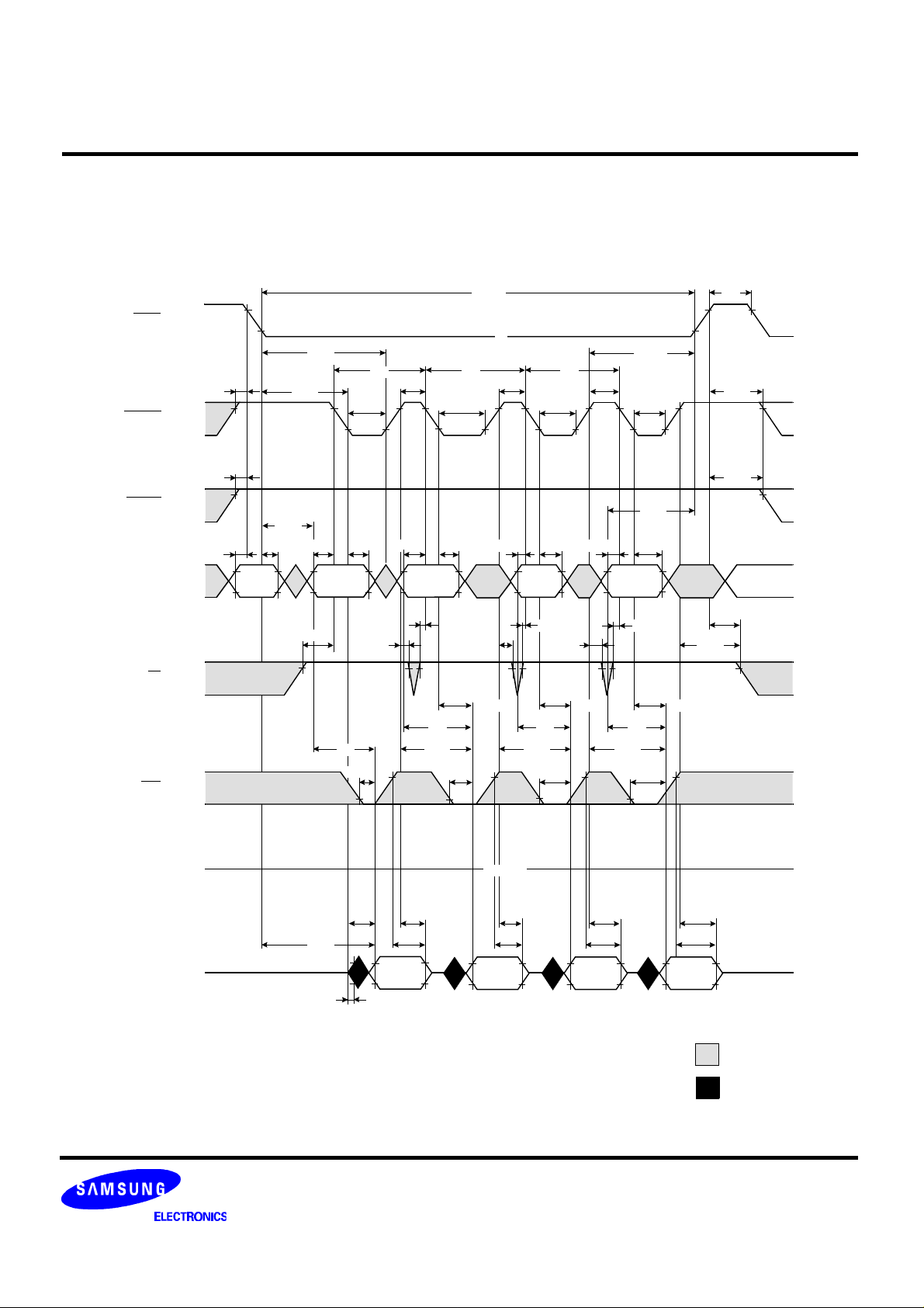
KM416C4000C, KM416C4100C CMOS DRAM
FAST PAGE MODE UPPER BYTE READ CYCLE
RAS
UCAS
LCAS
W
OE
A
VIH -
VIL -
VIH -
VIL -
VIH -
VIL -
VIH -
VIL -
VIH -
VIL -
VIH -
VIL -
tCRP
tCRP
tASR
tRASP
¡ó
tCSH
tPC tPC tPC
tRCD
tCP
tCP tCP
tCAS tCAS tCAS tCAS
tRAD
tRAH tASC tCAH tASC tCAH tCAH tCAH
ROW
ADDR
COLUMN
ADDRESS
tRCS
COLUMN
ADDRESS
tRCS
tRCH tRCH
tAA
tAA
tOEA
tCPA
tOEA
tCAC
tASC
tASC
COLUMN
ADDR
tRCS
tRCH
tCAC
tAA
tCPA
tOEA
tRHCP
tRAL
COLUMN
ADDRESS
tRCS
tAA
tCPA
tOEA
tRP
tRPC
tRPC
tRRH
tRCH
tCAC
DQ0 ~ DQ7
VOH -
VOL -
DQ8 ~ DQ15
VOH -
VOL -
tRAC
tCLZ
VALID
DATA-OUT
tOFF
tOEZ
OPEN
VALID
DATA-OUT
tOFF
tOEZ
VALID
DATA-OUT
tOFFtCAC
tOEZ
VALID
DATA-OUT
tOFF
tOEZ
Don′t care
Undefined
Page 25
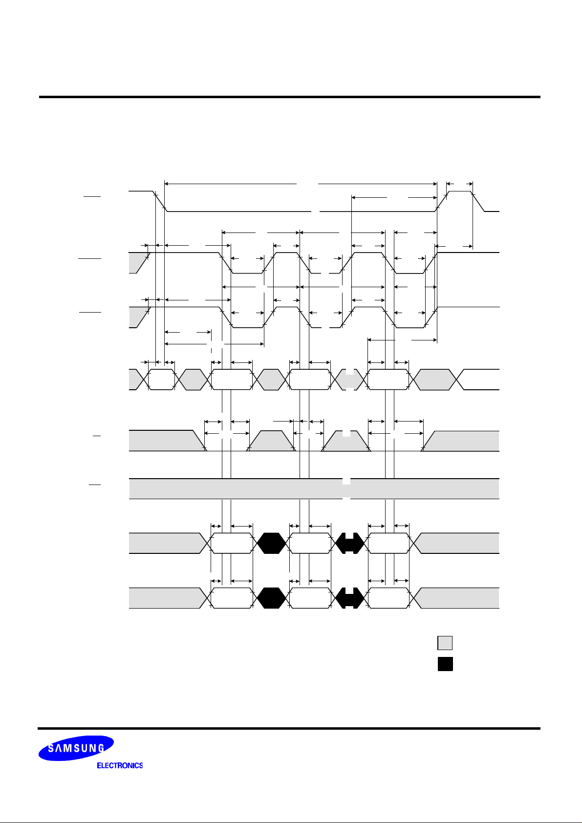
KM416C4000C, KM416C4100C CMOS DRAM
FAST PAGE MODE WORD WRITE CYCLE ( EARLY WRITE )
NOTE : DOUT = OPEN
tRASP tRP
RAS
VIH -
VIL -
¡ó
tRHCP
UCAS
LCAS
W
OE
A
VIH -
VIL -
VIH -
VIL -
VIH -
VIL -
VIH -
VIL -
VIH -
VIL -
tCRP
tCRP
tRCD
tRCD
tRAD
tCSH
tASR
tRAH tCAH tCAH tCAHtASC
ROW
ADDR
tASC
COLUMN
ADDRESS
tWCS tWCH
tWP
tPC tPC
tCP
tCAS
tPC tPC
tCP
tCAS
COLUMN
ADDRESS
tWCS tWCH
tWP
tCAS
¡ó
tCAS
¡ó
¡ó
¡ó
¡ó
¡ó
¡ó
tCP
tCAS
tCP
tRAL
tASC
COLUMN
ADDRESS
tWCS tWCH
tWP
tRSH
tCRP
tRSH
tCAS
DQ0 ~ DQ7
VIH -
VIL -
DQ8 ~ DQ15
VIH -
VIL -
tDS
tDH tDS tDH tDS tDH
VALID
DATA-IN
VALID
DATA-IN
¡ó
¡ó
tDH tDH tDHtDStDStDS
VALID
DATA-IN
VALID
DATA-IN
¡ó
¡ó
VALID
DATA-IN
VALID
DATA-IN
Don′t care
Undefined
Page 26
KM416C4000C, KM416C4100C CMOS DRAM
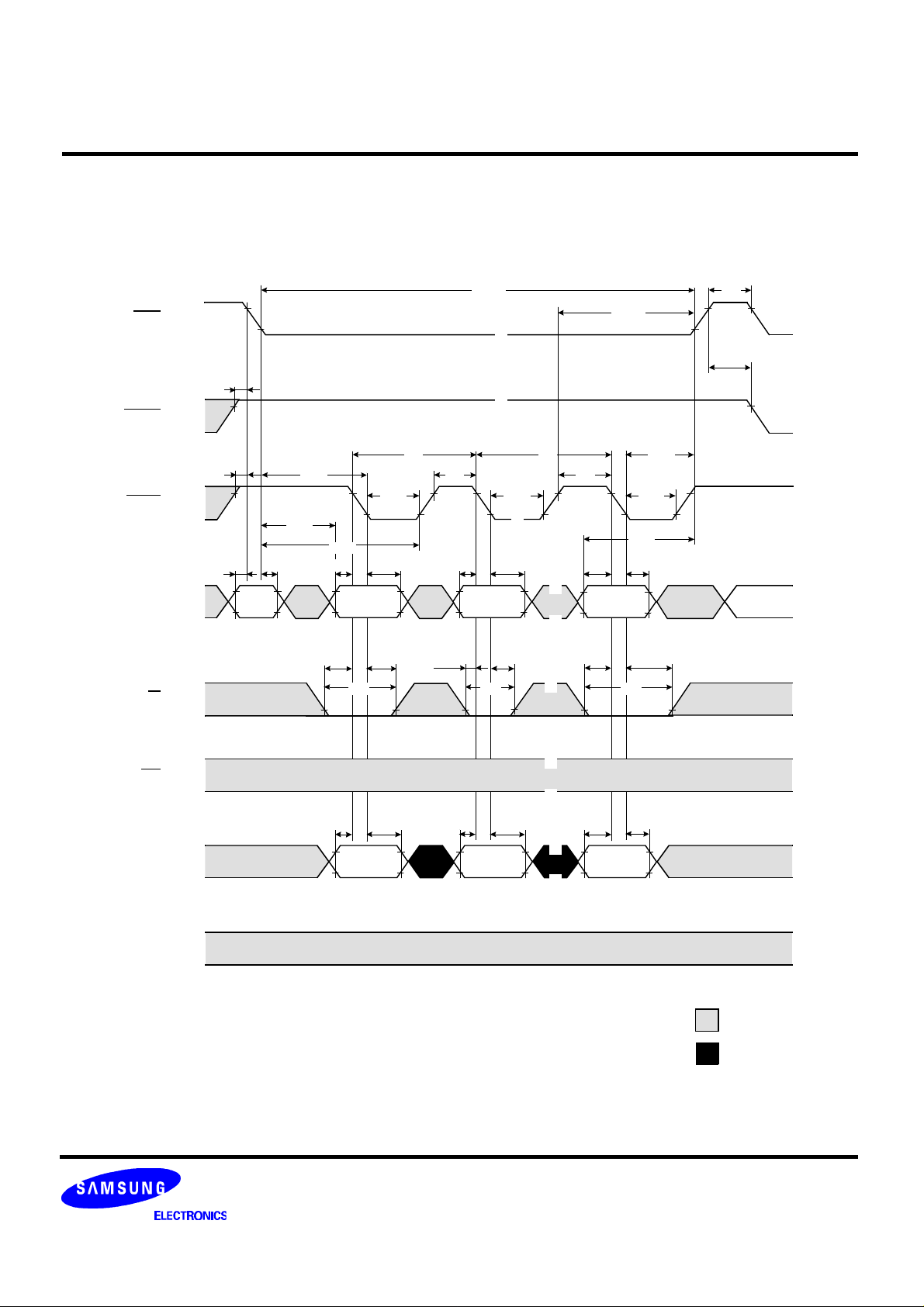
FAST PAGE MODE LOWER BYTE WRITE CYCLE ( EARLY WRITE )
NOTE : DOUT = OPEN
tRASP tRP
RAS
VIH -
VIL -
¡ó
tRHCP
UCAS
LCAS
W
OE
A
VIH -
VIL -
VIH -
VIL -
VIH -
VIL -
VIH -
VIL -
VIH -
VIL -
tCRP
tCRP
tASR
tPC tPC
tRCD
tCAS
tRAD
tCSH
tRAH tCAH tCAH tASC tCAHtASC
ROW
ADDR
tASC
COLUMN
ADDRESS
tWCS tWCH
tWP
¡ó
tCP
tCAS
COLUMN
ADDRESS
tWCS tWCH
tWP
tRPC
tRSH
tCP
tCAS
¡ó
tRAL
¡ó
COLUMN
ADDRESS
¡ó
tWCS tWCH
¡ó
¡ó
¡ó
tWP
DQ0 ~ DQ7
VIH -
VIL -
DQ8 ~ DQ15
VIH -
VIL -
tDS
tDH tDS tDH tDS tDH
VALID
DATA-IN
VALID
DATA-IN
¡ó
¡ó
VALID
DATA-IN
Don′t care
Undefined
Page 27
KM416C4000C, KM416C4100C CMOS DRAM
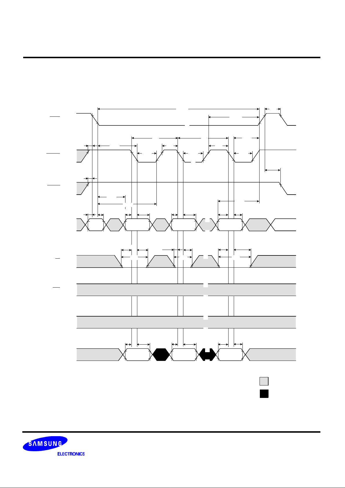
FAST PAGE MODE UPPER BYTE WRITE CYCLE ( EARLY WRITE )
NOTE : DOUT = OPEN
tRASP tRP
RAS
VIH -
VIL -
¡ó
tRHCP
UCAS
LCAS
W
OE
A
VIH -
VIL -
VIH -
VIL -
VIH -
VIL -
VIH -
VIL -
VIH -
VIL -
tCRP
tCRP
tASR
tPC tPC
tRCD
tCAS
tRAD
tCSH
tRAH tCAH tCAH tASC tCAHtASC
ROW
ADDR.
tASC
COLUMN
ADDRESS
tWCS tWCH
tWP
tCP
tCAS
COLUMN
ADDRESS
tWCS tWCH
tWP
tRSH
tCP
tCAS
¡ó
tRPC
tRAL
¡ó
COLUMN
ADDRESS
¡ó
tWCS tWCH
¡ó
¡ó
¡ó
tWP
DQ0 ~ DQ7
VIH -
VIL -
DQ8 ~ DQ15
VIH -
VIL -
¡ó
¡ó
tDS
tDH tDS tDH tDS tDH
VALID
DATA-IN
VALID
DATA-IN
¡ó
¡ó
VALID
DATA-IN
Don′t care
Undefined
Page 28
KM416C4000C, KM416C4100C CMOS DRAM
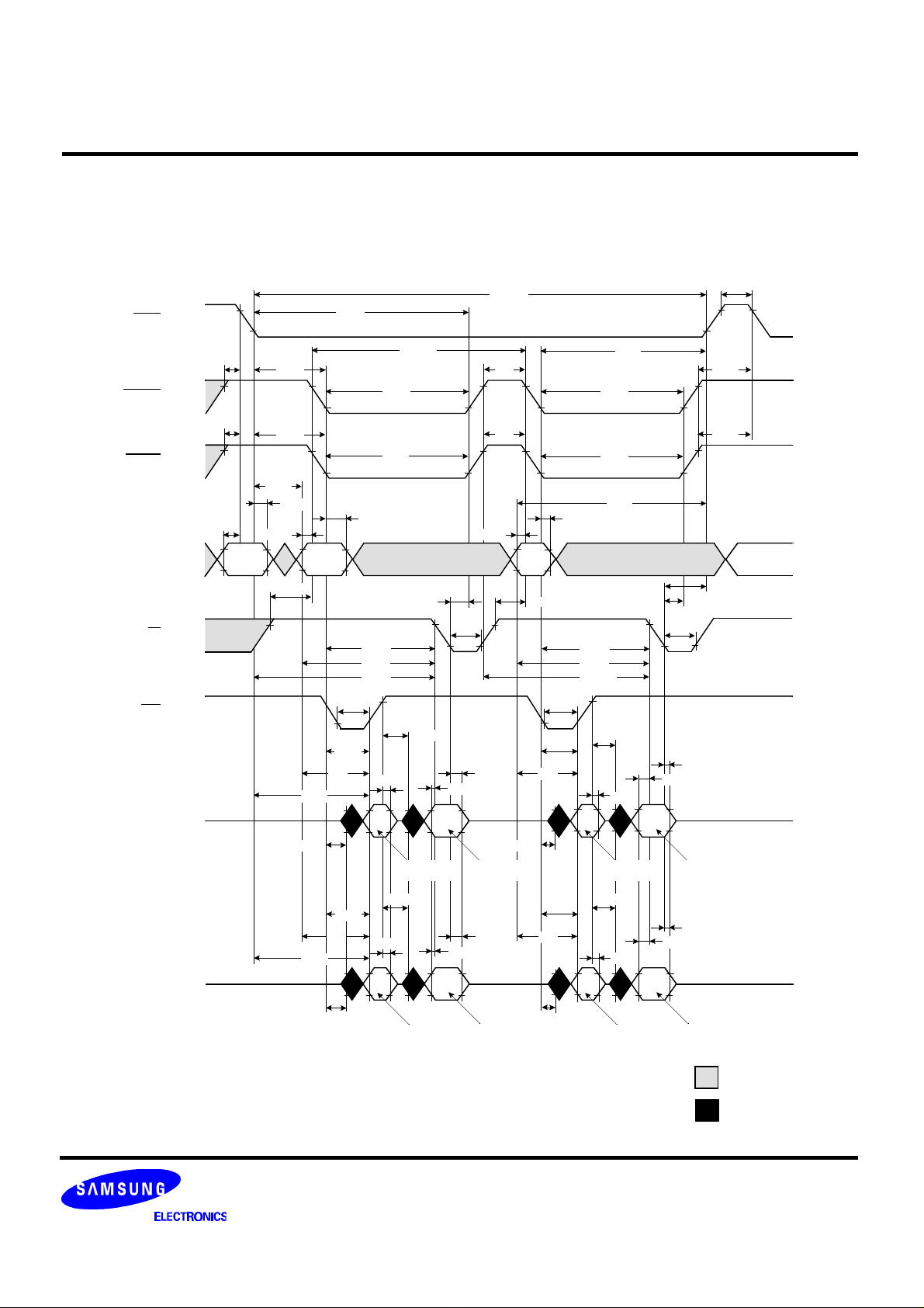
FAST PAGE MODE WORD READ-MODIFY-WRITE CYCLE
VIH -
RAS
VIL -
VIH -
UCAS
VIL -
VIH -
LCAS
VIL -
VIH -
A
VIL -
VIH -
W
VIL -
VIH -
OE
VIL -
DQ0 ~ DQ7
VI/OH -
VI/OL -
DQ8 ~ DQ15
VI/OH -
VI/OL -
tCRP
tCRP
tASR
tCSH
tPRWC
tRCD tCP
tCAS
tRCD tCP
tCAS
tRAD
tRAH
tCAH
tASC
ROW
ADDR
COL.
ADDR
tRCS
tCWL
tCWD
tAWD
tRWD
tOEA
tOED
tCAC
tAA
tOEZ
tRAC
tCLZ
VALID
DATA-OUT
tOED
tCAC
tAA
tOEZ
tRAC
tCLZ
DATA-OUT
VALID
tDS
tDS
tWP
tRASP
tASC
tDH
VALID
DATA-IN
tDH
VALID
DATA-IN
ADDR
tCLZ
tCLZ
COL.
tRCS
tAA
tAA
tOEA
tCAC
tCAC
tCAH
tCAS
tCAS
tCWD
tAWD
tCPWD
tOED
tOED
tRSH
tRAL
tRWL
tCWL
tOEZ
VALID
DATA-OUT
tOEZ
VALID
DATA-OUT
tDS
tDS
tWP
tDH
tDH
tCRP
tCRP
VALID
DATA-IN
VALID
DATA-IN
tRP
Don′t care
Undefined
Page 29
KM416C4000C, KM416C4100C CMOS DRAM
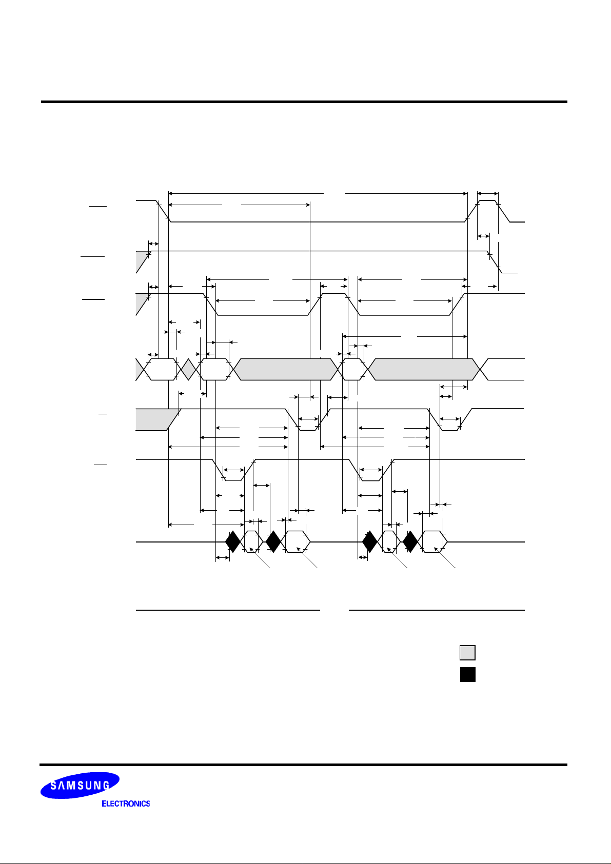
FAST PAGE MODE LOWER BYTE READ - MODIFY - WRITE CYCLE
VIH -
RAS
VIL -
VIH -
UCAS
VIL -
VIH -
LCAS
VIL -
VIH -
A
VIL -
VIH -
W
VIL -
VIH -
OE
VIL -
DQ0 ~ DQ7
VI/OH -
VI/OL -
DQ8 ~ DQ15
VI/OH -
VI/OL -
tCRP
tCRP
tASR
ROW
ADDR
tRCD
tRAD
tASC
tRCS
tRAH
tRAC
tCLZ
COL.
ADDR
tCSH
tCAC
tAA
tRASP
tCP
tCAS tCAS
tCAH
tASC
COL.
ADDR
tCWL
tWP
tCWD
tAWD
tRWD
tOEA
tOED
tOEZ
tDH
tDS
tCLZ
VALID
DATA-OUT
VALID
DATA-IN
OPEN
tRCS
tAA
tOEA
tCAC
tCAH
tCWD
tAWD
tCPWD
tOED
tRSHtPRWC
tRAL
tRWL
tCWL
tOEZ
VALID
DATA-OUT
tDS
tWP
tDH
tCRP
VALID
DATA-IN
tRP
tRPC
Don′t care
Undefined
Page 30
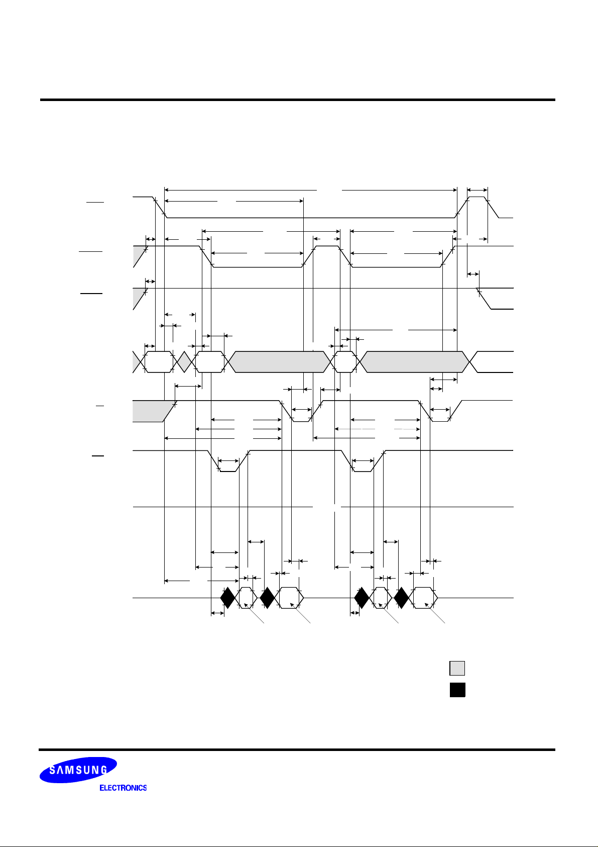
KM416C4000C, KM416C4100C CMOS DRAM
FAST PAGE MODE UPPER BYTE READ - MODIFY - WRITE CYCLE
RAS
UCAS
LCAS
OE
W
A
VIH -
VIL -
VIH -
VIL -
VIH -
VIL -
VIH -
VIL -
VIH -
VIL -
VIH -
VIL -
tCRP
tCRP
tASR
ROW
ADDR
tRCD
tRAD
tASC
tRAH
tRCS
COL.
ADDR
tCSH
tRASP
tCP
tCAS tCAS
tCAH
tASC
tCWL
tWP
tCWD
tAWD
tRWD
tOEA
COL.
ADDR
tRCS
tOEA
tCAH
tCWD
tAWD
tCPWD
tRSHtPRWC
tRAL
tRP
tCRP
tRPC
tRWL
tCWL
tWP
DQ0 ~ DQ7
VI/OH -
VI/OL -
DQ8 ~ DQ15
VI/OH -
VI/OL -
tRAC
tCLZ
tCAC
tAA
tOED
tOEZ
VALID
DATA-OUT
tDS
OPEN
tDH
VALID
DATA-IN
tCLZ
tAA
tCAC
tOED
tOEZ
VALID
DATA-OUT
tDS
tDH
VALID
DATA-IN
Don′t care
Undefined
Page 31
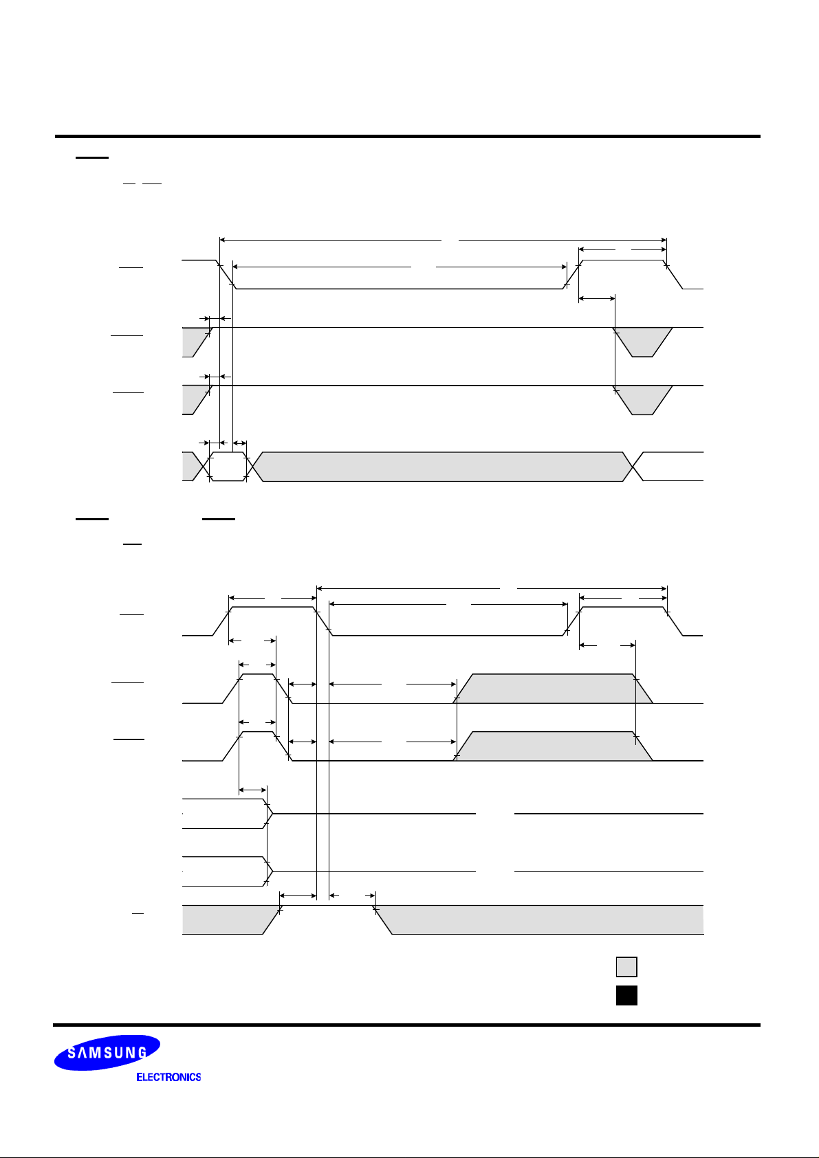
KM416C4000C, KM416C4100C CMOS DRAM
RAS - ONLY REFRESH CYCLE
NOTE : W, OE , DIN = Don′t care
DOUT = OPEN
VIH -
RAS
VIL -
tCRP
VIH -
UCAS
VIL -
tCRP
VIH -
LCAS
VIL -
A
tASR
VIH -
VIL -
tRAH
ROW
ADDR
CAS - BEFORE - RAS REFRESH CYCLE
NOTE : OE , A = Don′t care
tRP
tCRP
tCP
tCSR
tCP
tCSR
RAS
UCAS
LCAS
VIH VIL -
VIH VIL -
VIH VIL -
tCHR
tCHR
tRAS
tRC
tRAS
tRC
tRP
tRPC
tRP
tRPC
DQ0 ~ DQ7
VOH VOL -
DQ8 ~ DQ15
VOH -
VOL -
VIH -
W
VIL -
tOFF
tWRP
OPEN
OPEN
tWRH
Don′t care
Undefined
Page 32
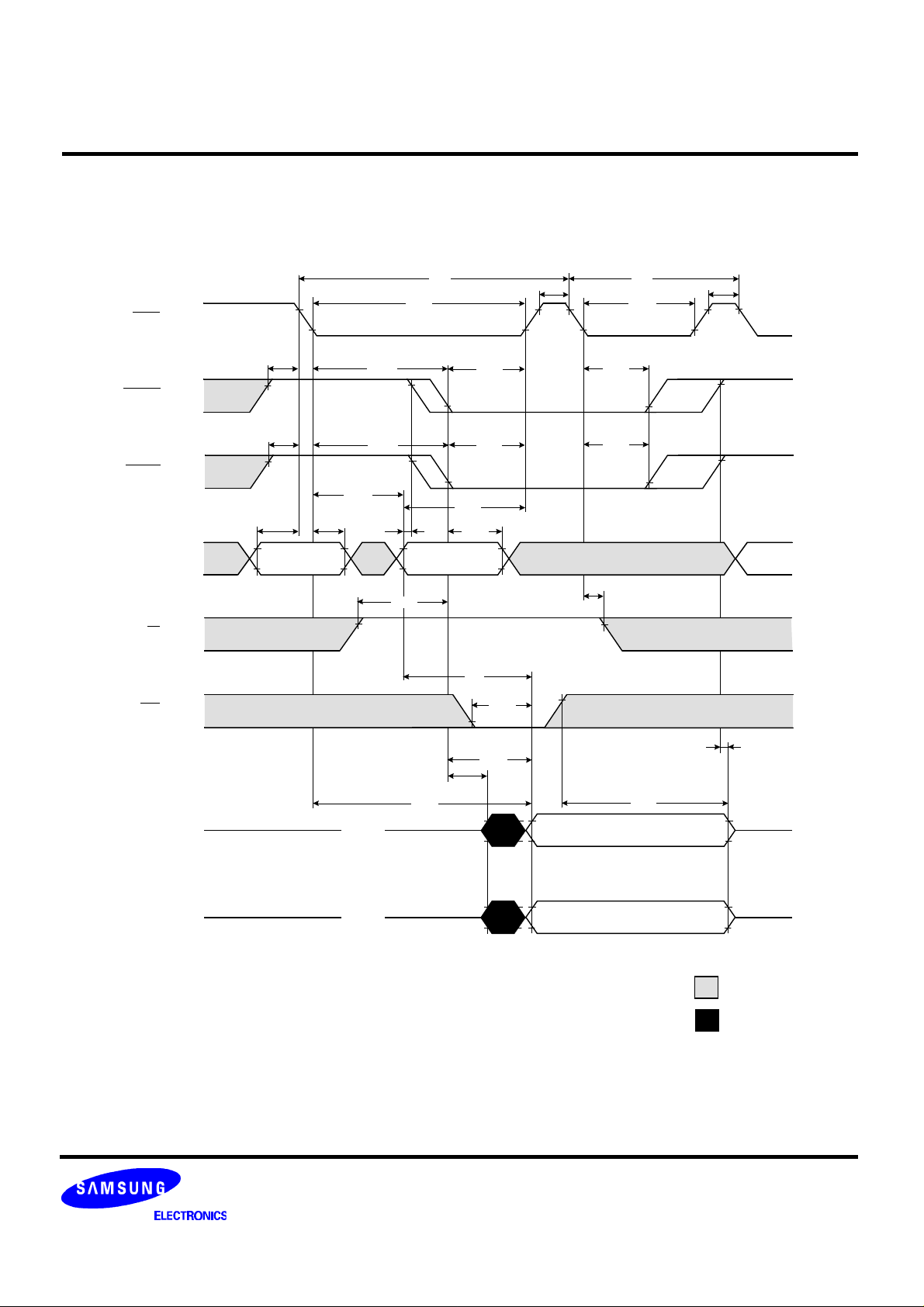
KM416C4000C, KM416C4100C CMOS DRAM
HIDDEN REFRESH CYCLE ( READ )
VIH -
RAS
VIL -
VIH -
UCAS
VIL -
VIH -
LCAS
VIL -
VIH -
A
VIL -
VIH -
W
VIL -
VIH -
OE
VIL -
DQ0 ~ DQ7
VOH -
VOL -
tCRP
tCRP
tRAD
tASR tRAH tASC
ROW
ADDRESS
OPEN
tRAS
tRCS
tRC
COLUMN
ADDRESS
tCLZ
tRAC
tRAL
tCAH
tAA
tRSHtRCD
tCAC
tOEA
tRP
tRC
tRAS
tCHRtRCD tRSH
tCHR
tWRH
tOEZ
DATA-OUT
tRP
tOFF
DQ8 ~ DQ15
VOH -
VOL -
OPEN
DATA-IN
DATA-OUT
Don′t care
Undefined
Page 33
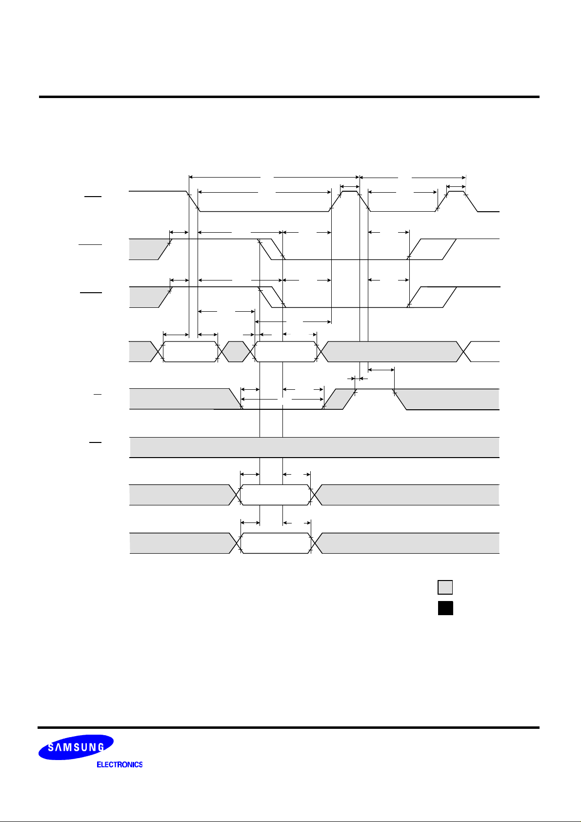
KM416C4000C, KM416C4100C CMOS DRAM
HIDDEN REFRESH CYCLE ( WRITE )
NOTE : DOUT = OPEN
VIH -
RAS
VIL -
VIH -
UCAS
VIL -
VIH -
LCAS
VIL -
VIH -
A
VIL -
VIH -
W
VIL -
VIH -
OE
VIL -
DQ0 ~ DQ7
VIH -
VIL -
tCRP
tCRP
tASR tRAH
ROW
ADDRESS
tRAD
tRCD
tASC
tWCS
tDS
tRC
tRAS
COLUMN
ADDRESS
DATA-IN
tWP
tRAL
tCAH
tDH
tRSH
tRSHtRCD
tWCH
tRP
tWRP
tCHR
tCHR
tRC
tRAS
tWRH
tRP
DQ8 ~ DQ15
VIH -
VIL -
tDS
tDH
DATA-IN
Don′t care
Undefined
Page 34
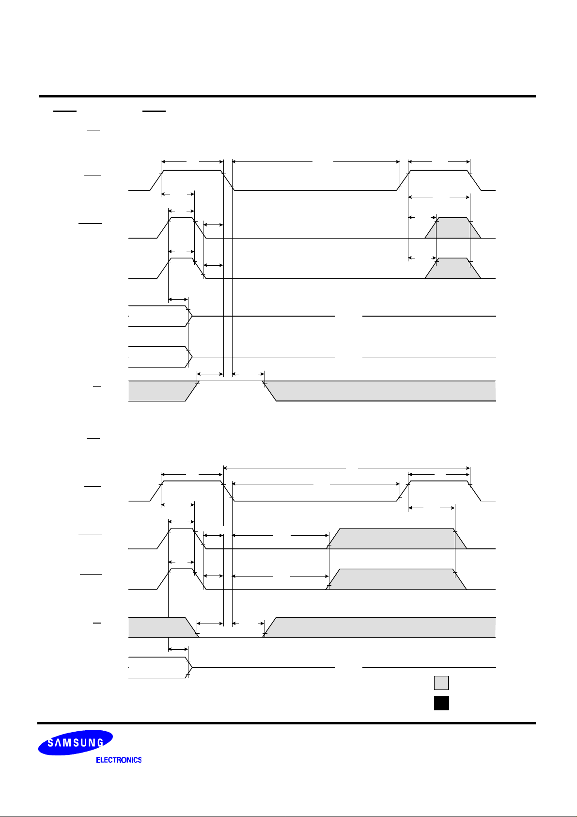
KM416C4000C, KM416C4100C CMOS DRAM
CAS - BEFORE - RAS SELF REFRESH CYCLE
NOTE : OE , A = Don′t care
VIH -
RAS
VIL -
VIH -
UCAS
VIL -
VIH -
LCAS
VIL -
DQ0 ~ DQ7
VOH VOL -
DQ8 ~ DQ15
VOH -
VOL -
VIH -
W
VIL -
tOFF
TEST MODE IN CYCLE
NOTE : OE , A = Don′t care
tRPC
tCP
tCP
tRP
tCSR
tCSR
tWRP
tWRH
tRASS
tRPS
tRPC
tCHS
tCHS
OPEN
OPEN
VIH -
RAS
VIL -
VIH -
UCAS
VIL -
VIH -
LCAS
VIL -
VIH -
W
VIL -
DQ0 ~ DQ15
VOH -
VOL -
tOFF
tCRP
tCP
tCP
tRP
tCSR
tCSR
tWTS
tWTH
tCHR
tCHR
tRAS
tRC
OPEN
tRP
tRPC
Don′t care
Undefined
Page 35
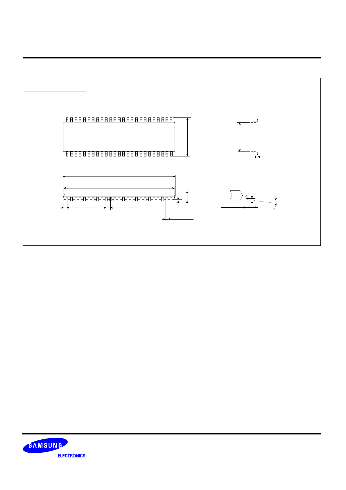
KM416C4000C, KM416C4100C CMOS DRAM
PLASTIC THIN SMALL OUT-LINE PACKAGE TYPE(II)
50 TSOP(II) 400mil
0.841 (21.35)
MAX
0.821 (20.85)
0.829 (21.05)
0.0315 (0.80)0.034 (0.875)
0.455 (11.56)
0.002 (0.05)
MIN
0.010 (0.25)
0.018 (0.45)
0.471 (11.96)
0.047 (1.20)
MAX
0.018 (0.45)
0.030 (0.75)
Units : Inches (millimeters)
0.400 (10.16)
0.004 (0.10)
0.010 (0.25)
0.010 (0.25)
TYP
0~8
O
 Loading...