

Page 1

DISCRETE SEMICONDUCTORS
DATA SH EET
KM110B/2
Magnetic field sensor
Preliminary specification
File under Discrete Semiconductors, SC17
Philips Semiconductors
November 1994
Page 2
Philips Semiconductors Preliminary specification
Magnetic field sensor KM110B/2
DESCRIPTION
The KM110B/2 is a sensitive magnetic field sensor,
employing the magnetoresistive effect in thin-film
permalloy. A Ferroxdure FXD100 magnet mounted on the
back of the sensor package provides an auxiliary field of
3.6 kA/m in the x-direction of the sensor.
Typical applications for the KM110B/2 are current
measurement, linear position measurement, rotational
speed detection of magnetic pole wheels as well as
magnetic field measurement. The sensor can be operated
at any frequency between DC and 1 MHz.
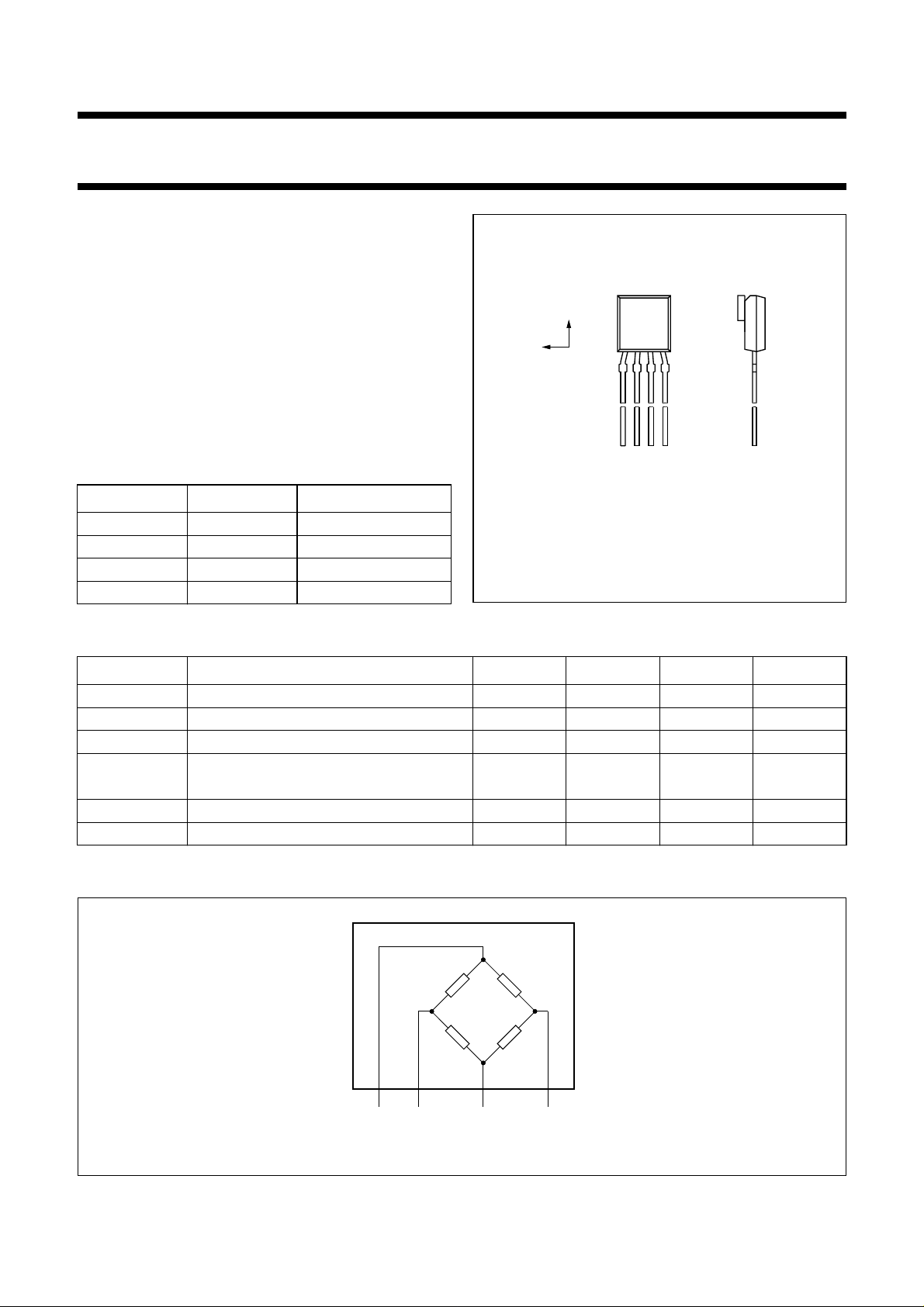
PINNING
PIN SYMBOL DESCRIPTION
1+V
O
output voltage
2 GND ground
3 −V
4+V
O
CC
output voltage
supply voltage
Marking: KMZ10B PHDxx.
x
y
1234
Fig.1 Simplified outline.
MLB874
QUICK REFERENCE DATA
SYMBOL PARAMETER MIN. TYP. MAX. UNIT
V
T
H
CC
bridge
y
DC supply voltage − 5 − V
bridge operating temperature −40 − 150 °C
magnetic field strength −2.2 − +2.2 kA/m
S sensitivity − 3.6 −
R
V
bridge
offset
bridge resistance 1.6 2.1 2.6 kΩ
offset voltage −0.5 − +0.5 mV/V
CIRCUIT DIAGRAM
MLB875
handbook, full pagewidth
43 2 1
mV V⁄
----------------kA m⁄
V
–V
CC
O
Fig.2 Simplified circuit diagram.
November 1994 2
GND
+V
O
Page 3

Philips Semiconductors Preliminary specification
Magnetic field sensor KM110B/2
LIMITING VALUES
In accordance with the Absolute Maximum Rating System (IEC 134).
SYMBOL PARAMETER CONDITIONS MIN. MAX. UNIT
V
CC
P
tot
T
stg
T
bridge
Note
1. Maximum operating temperature of the thin-film permalloy.
THERMAL CHARACTERISTICS
SYMBOL PARAMETER VALUE UNIT
R
th j-a
DC supply voltage − 12 V
total power dissipation up to T
amb
= 130 °C;
− 120 mW
see Fig.5
storage temperature note 1 −40 +150 °C
bridge operating temperature −40 +150 °C
thermal resistance from junction to ambient 180 K/W
CHARACTERISTICS
=25°C; VCC= 5 V unless otherwise specified.
T
amb
SYMBOL PARAMETER CONDITIONS MIN. TYP. MAX. UNIT
H
y
S sensitivity open circuit; notes 2 and 3 2.9 3.6. 4.4
TCV
O
R
bridge
TCR
bridge
magnetic field strength note 1 −2.2 − +2.2 kA/m
mV V⁄
----------------kA m⁄
temperature coefficient of
output voltage
VCC= −5V;
T
= −25 to +125 °C
amb
I
= 3 mA;
CC
T
= −25 to +125 °C
amb
−−0.4 − %/K
−−0.1 − %/K
bridge resistance 1.6 − 2.6 kΩ
temperature coefficient of
T
= −25 to +125 °C − 0.3 − %/K
bridge
bridge resistance
V
offset
TCV
offset
offset voltage −0.5 − +0.5 mV/V
temperature coefficient of
T
=−25 to +125 °C −5 ±1.5 5 (µV/V)/K
bridge
offset voltage
FL linearity deviation of output
voltage
H
0to±1 kA/m −−0.5 %⋅FS
y=
0to±1.6 kA/m −−1.7 %⋅FS
H
y=
H
=0to±2 kA/m −−2.0 %⋅FS
y
FH hysteresis of output voltage −−0.5 %⋅FS
f operating frequency note 4 0 − 1 MHz
November 1994 3
Page 4

Philips Semiconductors Preliminary specification
Magnetic field sensor KM110B/2
Notes to the characteristics
1. Magnet (Ferroxdure 100) delivers an auxiliary field of
Hx= 3.6 kA/m (temperature coefficient: −0.2 %/K).
Above 110 °C the auxiliary field Hx will be <3.0 kA/m;
stable sensor operation may be threatened by
disturbing magnetic fields.
at Hy1.6 kA/m=()V
V
O
=
2. .
S
-----------------------------------------------------------------------------------------------------------------
×
1.6 V
CC
at Hy0=()–
O
3. The sensitivity increases and decreases linear with the
supply voltage, thus the static output voltage is directly
proportional to the supply voltage.
4. Sensor bridge response only. When sensing high
speed rotation, the operating frequency may be
reduced due to eddy current effects.
handbook, halfpage
S
M
Hy
NS
Hx
V
O
(mV/V)
8
4
0
–4
handbook, halfpage
MBD885
M =direction ofmagnetization.
N, S = magnetic poles.
Fig.3 Principle of magnetization.
125
handbook, halfpage
P
tot
(mW)
100
75
50
25
4321
MBD892
MBD882
–8
–2 –1 0 2
T
amb
=25°C; V
offset
=0.
1
Hy(kA/m)
Fig.4 Sensor output characteristic.
November 1994 4
0
0
50 100
Fig.5 Power derating curve.
150
T
amb
o
( C)
200
Page 5

Philips Semiconductors Preliminary specification
Magnetic field sensor KM110B/2
PACKAGE OUTLINE
handbook, full pagewidth
1.8
max
5.2
max
12.7
max
0.66
0.56
0.35
4.8 max
4.6
4.4
chip
1234
1.25
(3x)
0.48
0.40
0.75
1.15
2.0
max
0.65
0.55
(2)
(1)
2.35
2.25
MBD881
0.4
min
Dimensions in mm.
(1) Terminal dimensions uncontrolled within this area.
(2) Position of sensor chip.
Fig.6 Outline of KM110B/2.
November 1994 5
Page 6

Philips Semiconductors Preliminary specification
Magnetic field sensor KM110B/2
DEFINITIONS
Data Sheet Status
Objective specification This data sheet contains target or goal specifications for product development.
Preliminary specification This data sheet contains preliminary data; supplementary data may be published later.
Product specification This data sheet contains final product specifications.
Limiting values
Limiting values given are in accordance with the Absolute Maximum Rating System (IEC 134). Stress above one or
more of the limiting values may cause permanent damage to the device. These are stress ratings only and operation
of the device at these or at any other conditions above those given in the Characteristics sections of the specification
is not implied. Exposure to limiting values for extended periods may affect device reliability.
Application information
Where application information is given, it is advisory and does not form part of the specification.
LIFE SUPPORT APPLICATIONS
These products are not designed for use in life support appliances, devices, or systems where malfunction of these
products can reasonably be expected to result in personal injury. Philips customers using or selling these products for
use in such applications do so at their own risk and agree to fully indemnify Philips for any damages resulting from such
improper use or sale.
November 1994 6
 Loading...