

Page 1

Version 1.0.1 Proprietary and Confidential
Longest Match Engine
KE5BLME008
Kawasaki LSI U.S.A., Inc.
Page 2

Version 1.0.1 Proprietary and Confidential
Table of Contents
1. Features ..........................................................................................................................1
Block Diagram................................................................................................................2
3. Pin Assignment and Description ....................................................................................3
3.1. Pin Assignment: Diagram...........................................................................................3
3.2. Pin Assignment: List .................................................................................................4
3.3. Pin Descriptions .........................................................................................................6
4. Functional Descriptions .................................................................................................8
4.1. Overview...................................................................................................................8
4.2. Reset .........................................................................................................................8
4.3. Initialization ..............................................................................................................9
4.4. Data Insertion............................................................................................................9
4.5. Search .......................................................................................................................9
4.6. Data Deletion...........................................................................................................12
4.7. Search via CPU Port................................................................................................12
4.8. Interruption..............................................................................................................12
4.9. Typical Operational Flow ........................................................................................13
5. DRAM...........................................................................................................................17
5.1. DRAM Specification...............................................................................................17
5.2. Connecting to DRAM..............................................................................................17
6. Register.........................................................................................................................18
6.1. Register Map...........................................................................................................18
6.2. Register Description ................................................................................................18
7. Command Description .................................................................................................21
8. Package Outline............................................................................................................27
9. Electrical Characteristics.............................................................................................28
9.1. Absolute Maximum Rating......................................................................................28
9.2. Operating Conditions...............................................................................................28
9.3. DC Characteristics...................................................................................................28
9.4. AC Characteristics...................................................................................................29
Page 3
Kawasaki LSI
8K Longest Match Search Engine (KE5BLME008) PRELIMINARY
Version1.0.1 Proprietary and Confidential
1
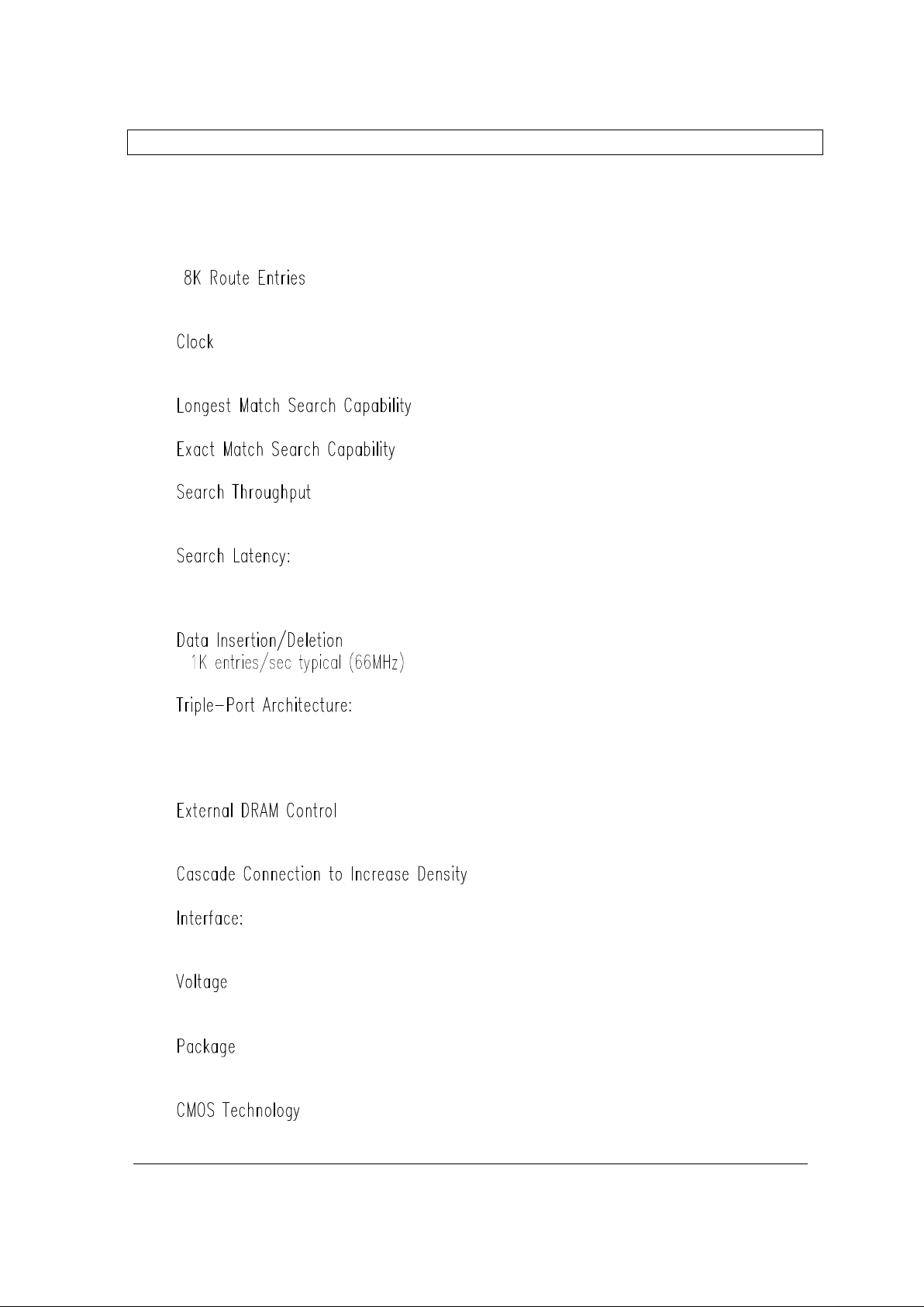
1. Features
The KE5BLME008 provides the best solution to a high-speed route search with the following
functions:
•
The device can store 8,192-route prefixes.
•
Maximum Clock Frequency: 66 MHz.
•
•
•
Maximum 4.1 Mpps (packet per sec. at 66MHz clock)
•
330 ns (hit flag; match length output)
420 ns (associative data output)
•
•
CPU port: 16 bit
Input port: 32 bit
Output port: 16 bit
•
16Mbit EDO DRAM
•
•
LVTTL
•
Single 3.3V ± 0.3V Supply
•
LQFP 176 Pin Package
•
Page 4
Kawasaki LSI
8K Longest Match Search Engine (KE5BLME008) PRELIMINARY
Version1.0.1 Proprietary and Confidential
2
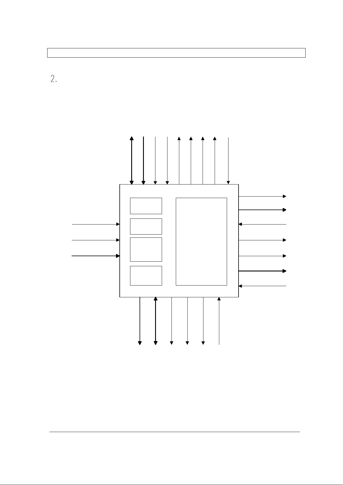
Block Diagram
Fig. 2.1 Block Diagram
DAT[15 : 0]
ADD[3 : 0]
CEN
RWN
RSTN
IRQN
OUT[15 : 0]
MDONEN
HON
OEN
FLN
AMFLN
MLE[4 : 0]
CLK
SRCHN
SDAT[3 1 :0]
CCMPN
DADD[9 :0]
DDAT[15 : 0]
DWEN
DRAS
DCAS
Registers
Search Table
8k Entries
Ins / Del
Queue
DRAM
Control
Control
Logic
CPU
Port
DRAM
Port
Input
Port
Output
Port
MLOEN
DRI
ODONEN
Page 5

Kawasaki LSI
8K Longest Match Search Engine (KE5BLME008) PRELIMINARY
Version1.0.1 Proprietary and Confidential
3
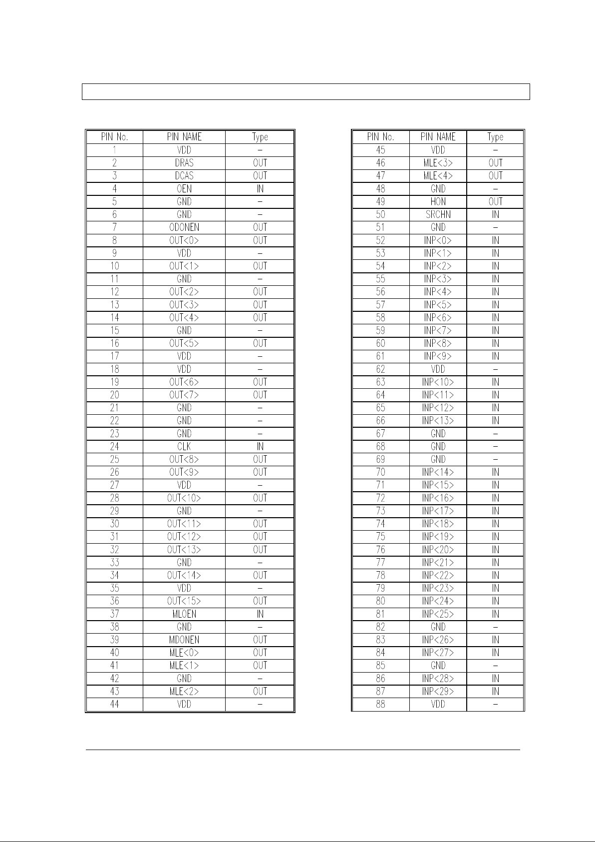
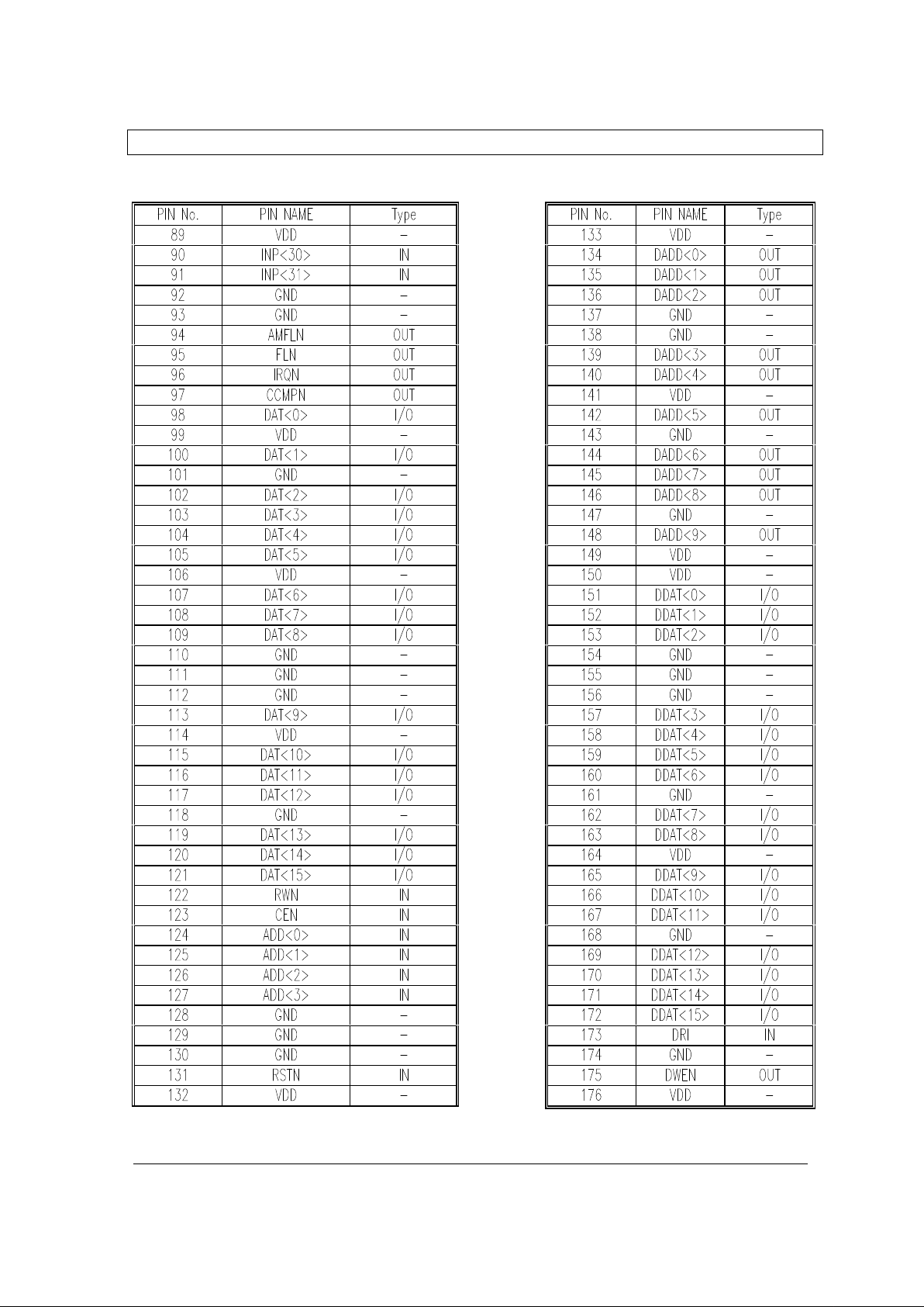
3. Pin Assignment and Description
3.1. Pin Assignment: Diagram
Fig. 3.1 Pin Assignment
44
1
INDEX
132 89
176
133
45
88
•• •••• ••
•• •••• ••
•• •••• ••
•• •••• ••
Page 6
Kawasaki LSI
8K Longest Match Search Engine (KE5BLME008) PRELIMINARY
Version1.0.1 Proprietary and Confidential
4
3.2. Pin Assignment: List
Table 3.1 Pin Assignment
Page 7
Kawasaki LSI
8K Longest Match Search Engine (KE5BLME008) PRELIMINARY
Version1.0.1 Proprietary and Confidential
5
Table 3.1 Pin Assignment (cont’d)
Page 8
Kawasaki LSI
8K Longest Match Search Engine (KE5BLME008) PRELIMINARY
Version1.0.1 Proprietary and Confidential
6
3.3. Pin Description
Pin Name Attribute Description # of Pins
CLK Clock
Input
LVTTL
CLK is the master clock input. Input
signals refer to the rising edge of CLK.
1
SRCHN Search Enable
Input
LVTTL
SRCHN enables a search operation;
search commences when Low is
signaled.
1
INP<31:0> Input Bus
Input
LVTTL
INP<31:0> is a 32-bit input bus used
for search key inputs.
32
OUT<15:0> Output Bus
Output
LVTTL
OUT<15:0>, a 16-bit output bus,
outputs the associate data.
16
OEN Output Enable
Input
LVTTL
OEN controls OUT<15:0>. OEN Low
enables OUT<15:0> ; and OEN High
enables High-Z.
1
ODONEN Output DONE
Output
LVTTL
ODONEN Low Active indicates that
the associate data is output to the OUT
<15:0> after a search.
1
HON Hit Output
Output
LVTTL
HON outputs a search result.
Low indicates a hit; High indicates a
miss hit.
1
MLE<4:0> Match Length
Output
LVTTL
MLE outputs match-length
information (prefix lengh-1) between
the data stored in the table and the
relevant search key.
5
MLOEN Match Length Output Enable
Input
LVTTL
MLOEN controls MLE<4:0> Output
Enable. Low enables MLE<4:0>;
High changes it to High-Z.
1
MDONEN MLE Done
Output
LVTTL
MDONEN Low indicates that the
completion of the search, outputting
the match length to MLE<4:0>.
1
RSTN Reset
Input
LVTTL
RSTN input Low resets the hardware. 1
IRQN Interrupt Request
Output
Open Drain
IRQN indicates Low when an interrupt
condition occurs in the CNTL register.
1
CCMPN Command Execution
Completion
Output
LVTTL
CCMPN signals High during the
command operation executed via CPU
port, and signals Low upon the
completion of its execution.
1
Page 9
Kawasaki LSI
8K Longest Match Search Engine (KE5BLME008) PRELIMINARY
Version1.0.1 Proprietary and Confidential
7
Pin Name Attribute Description # of Pins
ADD<3:0> CPU Port Address
Input
LVTTL
ADD<3:0> is a register address. 4
DAT<15:0> CPU Port Data Bus
Input
LVTTL
DAT<15:0> is an input/output data bus
for a CPU port.
16
CEN CPU Port Enable
Input
LVTTL
CEN serves as the CPU port access; CEN
Low enables the input operations of data
and command.
1
RWN Read/Write
Input
LVTTL
RWN determines the direction of the CPU
bus; RWN Low selects “write” cycle, and
RWN High “read” cycle.
1
FLN Full
Output
LVTTL
FLN outputs Low when all entries are
filled with valid data.
1
AMFLN Almost Full
Output
LVTTL
AMFLN outputs Low when reaching
“almost full”; the number of entries is
equal to or exceeds the value stored in the
Almost Full Register.
1
DADD <9:0> DRAM Address
Output
LVTTL
DADD outputs DRAM address. Ensure
that it is connected to the DRAM address
pins.
10
DDAT <15:0> DRAM Data
Input/Output
LVTTL
DDAT <15:0> is a bi-directional data bus
to DRAM. Ensure that it is connected to
the DRAM data input/output.
16
DWEN DRAM Write Enable
Output
LVTTL
DWEN is a DRAM Write Enable signal.
Ensure that it is connected to the DRAM
Write enable input.
1
DRAS DRAM RAS
Output
LVTTL
DRAS is a row address select signal to the
DRAM. Ensure that it is connected to the
RAS pin of DRAM.
1
DCAS DRAM CAS
Output
LVTTL
DCAS is a column address select signal to
the DRAM. Ensure that it is connected to
the relevant CAS pin of DRAM.
1
DRI RAS Timing Input
Input
LVTTL
RAS Timing Input controls DRAM
timing. Ensure that it is connected to the
DRAS pin.
1
VDD Supply The voltage required is 3.3V. 21
GND Ground Ground pin. 38
Page 10

Kawasaki LSI
8K Longest Match Search Engine (KE5BLME008) PRELIMINARY
Version1.0.1 Proprietary and Confidential
8
4. Functional Descriptions
4.1. Overview
KL5BLME008 is a search device for 32-bit IP address searches in IP routing applications. Its
capability extends beyond a simple lookup of data entries stored in a routing table. With its
compatibility with the CIDR (Classless Inter-Domain Routing), it outputs associated data for
the longest match data when there are multiple matching entries. KE5BLME008 also has the
search capability of finding the exact 32-bit match for searching the host address.
Moreover, LME008 provides a solution to routes having the same address with different
prefix length. Let us assume, for instance, the presence of both 192.1.0.0/16 and 192.1.0.0/24
in a routing table; the search key of 192.1.1.2 outputs associated data relative to 192.1.0.0/16
whereas the search key of 192.1.0.3 outputs ones relative to 192.1.0.0/24.
KL5BLME008 is a triple-port architecture equipped with task-specific ports: Input port
conducting a search, Output port effecting a result, and CPU port executing commands and
accessing to a register. This triple-port architecture facilities insertion and deletions of entries
without interrupting a search operation.
In order to store data, LME008 operates with an external 16Mbit EDO DRAM. Memory
control operations such as DRAM accesses and Refresh are, however, controlled by the
device itself.
4.2. Reset
The LME008 device requires a reset after chip power up. A reset can be applied by either
supplying a low pulse to the RSTN pins or writing any data onto a Reset register. The values
reassigned for both pins and registers are as follows:
Registers Pins
CNTL: 0000b IRQN: High-Z
STAT0: 1x00b FLN: High
STAT1: 0000b AMFLN: High
PR0 – RR2: Unknown CCMPN: Low
Almost Full Address: 0FFFh ODONEN: High
Refresh Counter Constant: 000001b (01h) MDONEN: High
HON: High
DWEN: High
DOEN: High
DRAS: High
DCAS: High
Page 11

Kawasaki LSI
8K Longest Match Search Engine (KE5BLME008) PRELIMINARY
Version1.0.1 Proprietary and Confidential
9
4.3. Initialization
After resetting the device, execute the Initialize command, which is required for data to be
properly inserted into the device. The execution of this command requires approximately
7.8µs at 66MHz clock. Before proceeding with the subsequent commands, check anew by
monitoring the CCMPN pin whether the initialization process has been completed.
4.4. Data Insertion
To enter data in the table, use the Insert command. Ensure that the IP address is set to WR01, the associated data to WR2, and PL (prefix length –1) to WR4.
Example:
When inserting 192.1.2.0/24 with associated data 3456h, enter the following.
WR0: 0200h (2.0)
WR1: C001h (192.1)
WR2: 3456h
WR4: 0017h (23 = 24–1)
Ensure that the value entered in WR4 is the prefix-length minus 1, not the prefix-length
itself.
The completion of the Insert command is confirmed by a low signal on the CCMPN pin.
Proceed with the subsequent commands after checking the CCMPN status.
LME008 is capable of storing the exact data match, i.e., the entry data hitting only when all
the 32 bits coincide with the input key data. When inserting exact match data, set 31 to WR4
(PL). This particular function is useful for storing the host address in the table.
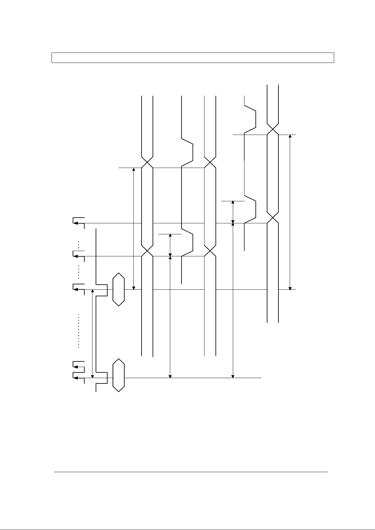
4.5. Search
To conduct a longest match search, apply data to INP [31:0], and set a SRCHN pin Low (see
Fig.4.1). At the 22nd clock after starting a search, MDONEN will be changed to Low,
allowing both MLE [4:0] and HON to output. MLE [4:0] output should be equal to the match
length minus one. That is to say, MLE [4:0] is the maximum value of the match length of a
search key minus 1. The HON status indicates a lookup result, with Low a hit, and High as a
miss hit. MDONEN will revert from High to Low after 4 clock cycles, while both MLE [4:0]
and HON will be held until the next lookup result.
At the 28th clock after starting a search, ODONEN will be changed into Low, allowing OUT
[15:0] to output associated data. If the search results in a miss match, the value pre-registered
at the default associated data will be returned. ODONEN will revert from High to Low after
4 clock cycles, whereas OUT [15:0] will be held until the next result. For instance, let us
assume the presence of the following data in the table:
Page 12
Kawasaki LSI
8K Longest Match Search Engine (KE5BLME008) PRELIMINARY
Version1.0.1 Proprietary and Confidential
10
133.5.0.0/16 [associated data: 1111h]
133.5.16.0/24 [associated data: 2222h]
Cf. Default associated data: 0000h
The result is as follows:
Search Key Result HON status MLE[4:0] OUT[15:0]
133.5.16.2 Hit at
133.5.16.0/24
Low 23 (17h) 2222h
133.5.17.3 Hit at
133.5.0.0/16
Low 15 (0fh) 1111h
133.6.0.1 Miss hit* High 0 0000h
Note: “*” indicates that133.5.0.0 and 133.6.0.1 have the matching length of 14-bits; a
miss hit occurs because the matching length is shorter than the registered value of
“16.”
Page 13
Kawasaki LSI
8K Longest Match Search Engine (KE5BLME008) PRELIMINARY
Version1.0.1 Proprietary and Confidential
11
CLK
SRCHN
INP<31:0>
HON
MDONEN
MLE<4:0>
ODONEN
OUT<15:0>
28 Clocks
4 Clocks
Key1 Key2
Search result of Key 1
Search result of Key 1
Search result of Key 1
Search result of Key 2
Search result of Key 2
Search result of Key 2
16 Clocks min.
4 Clocks
22 Clocks
22 Clocks
28 Clocks
Fig. 4.1 Search Timing
Page 14

Kawasaki LSI
8K Longest Match Search Engine (KE5BLME008) PRELIMINARY
Version1.0.1 Proprietary and Confidential
12
4.6. Data Deletion
To delete data from the table, use the Delete command. Ensure that the IP address is set to
WR0-1, and PL to WR4 with a prefix-length minus 1 before executing the commands.
Example:
If deleting 192.1.2.0/24, set the registers as follows.
WR0: 0200h (2.0)
WR1: C001h (192.1)
WR4: 0017h (23 = 24–1)
Notes:
l Ensure that the value set to WR4 is the prefix-length minus 1, not the prefix-length
itself.
l No deletion can be performed if the value entered to WR4 differs from that of the
initial entry. For instance, if 0018h is entered to WR4 followed by the Delete
command execution, 192.1.2.0/24 will not be deleted and will remain in the table.
The completion of the Delete command will be confirmed by a low status of CCMPN pin.
Before proceeding with the subsequent commands, check anew to confirm that the Delete
command execution has finished.
4.7. Search via CPU Port
A search can be performed with the CPU port commands, independently of the Input port
operation. Apply a search key data to WR0-1 to execute the Search command. Upon
completion of a table lookup, associated data will be written to RR0; and both ML (prefixlength minus one) and hit-or-miss-hit information will be written to RR2. The command
execution can be confirmed by monitoring the CCPN pin status; before proceeding with
subsequent commands, ensure that the CCMPN pin is changed to Low.
4.8. Interruption
To conduct interruption or a series thereof, set a CNTL register. Interruption is not
accomplished unless one of the conditions is met, as described in “6.2. Register
Description.” For instance, setting both bit 2 and bit 0 of a CNTL register to “1” activates
the Interrupt operation upon completion of either the Initialize command or the table
fulfillment process. To clear Interrupt, read STAT1, which should revert each bit to “0.”
Page 15

Kawasaki LSI
8K Longest Match Search Engine (KE5BLME008) PRELIMINARY
Version1.0.1 Proprietary and Confidential
13
Notes:
l The Interrupt operation set to the bit 3 occurs ONLY after the executions of
Search/Insert/Delete commands. No other commands are valid.
l The Interrupt operation set to the bit 2 occurs ONLY after the execution of the
Initialize command. No other commands are valid.
l The Interrupt operation set to the bit 1 occurs ONLY after the execution of either
the Insert or Delete command when the values registered in the Entry Count match
those of the Almost Full Register. See the example below:
Example: Entry Count = 999 (3E7h)/Almost Full Register = 1000 (3E8h)
Command Entry Count Interruption AMFLN
Insert 1000 Generated Low
â
Insert 1001 Not generated Low
â
Insert 1002 Not generated Low
â
Delete 1001 Not generated Low
â
Delete 1000 Generated Low
â
Delete 999 Not generated High
l The Interrupt operation set to the bit 0 occurs ONLY after the table becomes full.
4.9. Typical Operational Flow
(1) Turn on the power.
(2) Reset
Input a Low pulse to a RSTN.
(3) Initialize.
Write “Initialize” (0004h) onto the COM register (00h).
Wait for CCMPN to turn to Low.
(4) Set a Refresh Counter:
(a) Write 001Dh onto the WR0 (04h).
(b) Write the Set Refresh Counter Constant (06h) onto the COM register (00h).
(c) Wait for CCMPN to turn to Low.
Note: In case of 66MHz, Refresh Cycle Time will be (31+1) * 484.8ns
=15.51µs.
Page 16

Kawasaki LSI
8K Longest Match Search Engine (KE5BLME008) PRELIMINARY
Version1.0.1 Proprietary and Confidential
14
(5) Set the default associate data:
(a) Write “FFFFh” onto WR0 (04h).
(b) Write “Set Default Associated Data” (0007h) onto the COM register (00h).
(c) Wait for the CCMPN to Low.
(6) Data Insertion 1
(a) Write 0000h onto WR0 (04h).
(b) Write C018h onto WR1 (05h).
(c) Write 1111h onto WR2 (06h).
(d) Write 14h onto WR4 (08h).
(e) Write Insert (0002h) onto the COM register (00h).
(f) Wait for CCMPN to turn to Low; 192.24.0.0/21 will be registered with associated
data 1111h in a table.
(7) Data Insertion 2
(a) Write 0800h onto the WR0 (04h).
(b) Write C018 onto the WR1 (05h).
(c) Write 2222h onto the WR2 (06h).
(d) Wrote 15h onto the WR4 (08h).
(e) Write Insert (0002h) onto the COM register (00h).
(f) Wait for CCMPN to turn to Low; 192.24.8.0 /22 will be registered with associated
data 2222h in the table.
(8) Data Input 3
(a) Write 000h onto the WR0 (04h).
(b) Write C018h onto the WR1 (05h).
(c) Write 0000h onto the WR2 (06h).
(d) Write 0Ch onto the WR4 (08h).
(e) Write Insert (0002h) onto the COM register (00h).
(f) Wait for the CCMPN to turn to Low; 192.24.0.0/13 will be registered in the table
with associated data 0000h.
(9) Data lookup 1
Start with 192.24.1.2 (C0180102h):
Result Hit
HON Low
MLE [4:0] 14h
OUT [15:0] 1111h
Page 17

Kawasaki LSI
8K Longest Match Search Engine (KE5BLME008) PRELIMINARY
Version1.0.1 Proprietary and Confidential
15
(10) Data Lookup 2
Start with 192.25.1.2 (C0190102h):
Result: Hit
HON: Low
MLE [4:0] 0Ch
OUT [15:0] 0000h
(11) Data Lookup 3
Start with 192.24.10.11(C0180A0Bh):
Result: Hit
HON: Low
MLE [4:0] 15h
OUT [15:0] 2222h
(12) Data Lookup 4
Start with 193.24.10.11 (C1180A0Bh):
Result: Miss Hit
HON: High
MLE [4:0] 00h
OUT [15:0] FFFFh
(13) Data Insertion 4
(a) Write 0102h onto WRO (04h).
(b) Write c018h onto WR1 (05h).
(c) Write 1234h onto WR2 (06h).
(d) Write 1Fh onto the WR4 (08h).
(e) Write Insert (0002h) onto the COM register (00h); the Host Address 192.24.1.2 will
be stored with associated data 1234h.
(14) Data Lookup 5
Start with 192.24.1.2 (C0180102h):
Result: Hit
HON: Low
MLE [4:0] 1Fh
OUT [15:0] 1234h
Page 18

Kawasaki LSI
8K Longest Match Search Engine (KE5BLME008) PRELIMINARY
Version1.0.1 Proprietary and Confidential
16
(15) Data Lookup 6
Start with 192.24.1.3 (V0180103h):
Result: Hit
HON: Low
MLE [4:0] 1Fh
OUT [15:0] 1111h
(16) Data Deletion
(a) Wait for the CCMPN to turn to Low.
(b) Write 0000h onto the WR0 (04h).
(c) Write C018 onto the WR1 (05h).
(d) Write 0000h onto the WR2 (06h).
(e) Write 0Ch onto the WR4 (08h).
(f) Write Delete (0003h) onto the COM register (00h); 192.24.0.0/13 will be deleted.
(17) Data Lookup 7
Start with 192.25.1.2 (C0190102h):
Result: Miss Hit
HON: High
MLE [4:0] 00h
OUT [15:0] FFFFh
Page 19

Kawasaki LSI
8K Longest Match Search Engine (KE5BLME008) PRELIMINARY
Version1.0.1 Proprietary and Confidential
17
5. DRAM
5.1. DRAM Specification
When using KE5BLME008, ensure that the corresponding DRAM meets the following
requirements:
16Mbit EDO DRAM (1M-word x 16-bit)
l Row x Column = 4096 x 256
l Voltage: 3.3V
l RAS access time: 60ns
Eg. Toshiba TC51V16165CFTS-60
5.2. Connecting to DRAM
For the connection of LME008 to DRAM, see Fig. 5.1 below. LME008 and DRAM should be
closely situated, so that the wiring between the two can be shortened. Ensure that the DRI is
connected to DRAS, and the OE of the DRAM is pulled down.
Fig. 5.1 Connection to DRAM
DADD[9:0]
DDAT[15:0]
DRAS
DRI
DCAS
DWEN
/RAS
/CAS
/WE
DAT[15:0]
ADD[9:0]
LME008 DRAM
/OE
ADD[11:10]
Page 20

Kawasaki LSI
8K Longest Match Search Engine (KE5BLME008) PRELIMINARY
Version1.0.1 Proprietary and Confidential
18
6. Register
6.1. Register Map
Table 6.1 Register Address
6.2. Register Description
COM (Command Register)
Write Only
ADD [3:0] = 0h:
Write the 16-bit OP code below in the COM register for a command execution:
Command OP Code Use Register
NOP 0000h Search 0001h WR0,WR1, RR0, RR2
Insert 0002h WR0, WR1, WR2, WR4
Delete 0003h WR0, WR1,WR4
Initialize 0004h Set Almost Full Register 0005h WR0
Set Refresh Counter Cnstant 0006h WR0
Set Default Associative Data 0007h WR0
Write DRAM 0008h WR0, WR1, WR2
Read Almost Full Register 0015h RR0
Read Refresh counter constant 0016h RR0
Read Default Attribute 0017h RR0
Read DRAM 0018h WR0 , WR1, RR0
Read Entry Data 001Ah WR0, RR0, RR1
Return Entry Count 001Bh RR0
Table 6.2 OP Code
Register name Address Type
COM 0h Write
CNTL 1h R/W
STAT0 2h Read
STAT1 3h Read
WR0 4h Write
WR1 5h Write
WR2 6h Write
WR3 7h Reserved
WR4 8h Write
RR0 9h Read
RR1 Ah Read
RR2 Bh Read
RESET Fh Write
Page 21

Kawasaki LSI
8K Longest Match Search Engine (KE5BLME008) PRELIMINARY
Version1.0.1 Proprietary and Confidential
19
STAT0 (Status Register):
ADD [3:0] = 01h:
bit 3 1: Last command complete / 0: Not yet complete
bit 2 1: CPU search hit / 0: CPU search miss hit
bit 1 1: Table almost full / 0:Table not almost full
bit 0 1: Table full / 0:Table not full
Default Value 1x00b
Bit 2 is valid after the Search command is executed until the next command is engaged.
STAT1 (Interrupt Status Register):
ADD [3:0] = 02h:
bit 3 1: Completion of Search/Ins/Del command
bit 2 1: Completion of the Initialize command
bit 1 1: Table reaching the almost full point
bit 0 1: Table reaching full
Default Value 0000b
This register will be cleared after reading is completed.
IRQN will be cleared when this register is read.
CNTL (Control Register):
ADD [3:0] = 03h:
Controls the configuration of an Interrupt operation.
bit 3 1: Enables interruption on the Completion of Search/Ins/Del command
bit 2 1: Enables interruption on the Completion of Initialize command
bit 1 1: Enables interruption on Table reaching almost full point
bit 0 1: Enables interruption on Table reaching full
Default Value 0000b
Page 22

Kawasaki LSI
8K Longest Match Search Engine (KE5BLME008) PRELIMINARY
Version1.0.1 Proprietary and Confidential
20
WR0-4 (Write Register):
WR0: ADD[3:0] = 04h
WR1: ADD[3:0] = 05h
WR2: ADD[3:0] = 06h
WR3: ADD[3:0] = 08h
Stores the data required for the command executions. See Table 6.2, “OP Code” for
registers specific to each command.
RR0-2 (Read Register):
RR0: ADD[3:0] = 09h
RR1: ADD[3:0] = 0Ah
RR2: ADD[3:0] = 0Bh
The data set to RR0-RR2 is valid until the next command is engaged.
RR0-RR2 has unknown values when the command with no return value to these registers is
executed.
RESET (Reset Register):
ADD [3:0] =0Fh
Write onto this register to activate the Reset command. This operation is the same as the
RSTN pin requiring a low pulse input.
Page 23

Kawasaki LSI
8K Longest Match Search Engine (KE5BLME008) PRELIMINARY
Version1.0.1 Proprietary and Confidential
21
7. Command Description
Writing the OP code onto the COM register (00h) enables a command execution. Upon
completion of the command execution, bit3 of STAT0 will be changed to 1, and CCMPN to
Low. Throughout the execution of a particular command, the execution of the other
commands is prohibited; and rewriting to the WR register is also prohibited. Should rewriting
to either the WR register or the COM register occur, the proper command execution may not
be maintained.
NOP (OP Code: 0000h):
No operation.
Search(OP Code: 0001h):
When this command is executed, a lookup operation starts with a key value in WR0-1.
Upon completion of this command, associated data is written to RR0, and ML (Match
Length minus 1) to RR2, setting a bit 3 (Command Complete) of STAT0 to 1. The bit 15 of
RR2(H) shows a lookup result, registering either “1” as a hit or “0” as a miss hit.
WR1 WR0
15 0 15 0
IP Address (31 -16 ) IP Address ( 15 - 0)
RR0
15 0
Associated Data ( 15 - 0)
RR2
15 4 0
H ML ( 4-0 )
Page 24

Kawasaki LSI
8K Longest Match Search Engine (KE5BLME008) PRELIMINARY
Version1.0.1 Proprietary and Confidential
22
Insert (OP Code: 0002h):
To execute this command, write the entry data (IP address) to WR0-WR1, the associated
data to WR2, and the PL (Prefix Length minus 1) to WR4. The execution of this command
prompts storing these data to the table. When the insertion is completed, bit3 of STAT0
will be changed to ‘1,’ and CCMPN to Low.
WR1 WR0
15 0 15 0
IP Address (31 -16 ) IP Address ( 15 - 0)
WR2
15 0
Associated Data ( 15 - 0)
WR4
4 0
PL( 4-0 )
Delete (OP Code: 0003h):
To execute this command, write the entry data (IP address) to WR0-WR1and PL (Prefix
Length minus 1) to WR4. The execution of this command prompts deleting the data from
the table. Upon completion of the data deletion, bit3 of STAT0 will be changed to ‘1,’ and
CCPMN to Low.
WR1 WR0
15 0 15 0
IP Address (31 -16 ) IP Address ( 15 - 0)
WR4
4 0
PL( 4-0 )
Page 25

Kawasaki LSI
8K Longest Match Search Engine (KE5BLME008) PRELIMINARY
Version1.0.1 Proprietary and Confidential
23
Initialize (OP Code: 0004h):
This command clears all entries, after which the table will become empty.
Upon completion of the command, the CNTL Register, Almost Full Register, and Refresh
Counter Constant will maintain their current value, while STAT0 will have the Default; bit
3 of STAT0 (Command Complete) will be changed to 1, and CCMPN to Low. This
command execution requires approximately7.8µs at 66MHz.
Set Almost Full Register (OP Code: 0005h):
The value in WR0 is set to Almost Full Register. Upon completion of the command, bit3 of
STAT0 (Command Complete) will be changed to ‘1,’ and CCMPN is changed to Low.
When the number of entries is greater than or equal to the Almost Full Register value,
AMFLN will be changed to Low with bit1of STAT0 set to ‘1.‘ Interrupt is activated when
the number of entries is equal to the Almost Full Register value.
WR0
12 0
Almost Full Entry Count ( 12-0 )
Default Value of Almost Full register is 0FFFh.
Read Almost Full Register (OP Code: 0015h):
The value in Almost Full register is set to RR0.
Upon completion of the data setting to RR0, bit3 of STAT0 (Command Complete) is
changed to ‘1,' and CCMPN to Low.
RR0
12 0
Almost Full Entry Count ( 12-0 )
Page 26

Kawasaki LSI
8K Longest Match Search Engine (KE5BLME008) PRELIMINARY
Version1.0.1 Proprietary and Confidential
24
Set Refresh Counter Constant (OP Code: 0006h):
The value in WR0 is set as the Refresh Counter Constant.
When the internal counter is equal to the Refresh Counter Constant, Refresh is executed,
and the internal counter cleared. 6 LSB bits are valid. Upon completion of the data input to
the internal register, bit3 of STAT0 will be changed to ‘1,’ and CCMPN to Low.
Refresh cycle time = (Refresh Counter Constant +1) * Trfc
Trfc = 1/f * 32 ( f : Clock Frequency )
Example:
f = 66 MHz
Trfc = 484.8 ns
RCC = 31 (011111b)
Refresh Cycle Time = 32 * 484.8 ns = 15.51 us
WR0
5 0
RCC ( 5-0 )
RCC : Refresh Counter Constant
Default : 000001 b
Read Refresh Counter Constant (OP Code: 0016h):
Current Refresh Counter Constant is written to RR0. Upon completion of the data setting to
PR0, bit3 of STAT0 will be changed to ‘1,’ and CCMPN to Low.
RR0
5 0
RCC ( 5-0 )
RCC : Refresh Counter Constant
Page 27

Kawasaki LSI
8K Longest Match Search Engine (KE5BLME008) PRELIMINARY
Version1.0.1 Proprietary and Confidential
25
Set Default Associated Data (OP Code: 0007h):
The value in WR0 is set as the default associated data, which is output when a miss hit
occurs. Upon completion of the data input to the internal register, bit3 of STAT0 will be
changed to ‘1,’ and CCMPN to Low.
WR0
15 0
Default Associated Data ( 15 - 0)
Read Default Associated Data (OP code: 0017h):
The Default Associate Data is written to RR0.
Upon completion of the data setting to RR0, bit3 of STAT0 (Command Complete) will be
changed to ‘1,’ and CCMPN to Low.
RR0
15 0
Default Associate Data ( 15 – 0)
Write DRAM (OP Code: 0008h):
The data in WR2 is written to DRAM.
The address of DRAM is specified by the value in WR0-WR1.
Upon the completion of the command, bit3 of STAT0 will be changed to ‘1,’ and CCMPN
to LOW.
WR1 WR0
1 0 15 0
DRAM Address (17 –16 ) DRAM Address ( 15 – 0)
WR2
15 0
DRAM Data ( 15 – 0)
Page 28

Kawasaki LSI
8K Longest Match Search Engine (KE5BLME008) PRELIMINARY
Version1.0.1 Proprietary and Confidential
26
Read DRAM (OP Code: 0018h):
The data of DRAM is read and written to RR0; the address of DRAM is specified by the
value in WR0-WR1. Upon completion of the command, bit3 of STAT0 will be changed to
‘1,’ and CCMPN to Low.
WR1 WR0
1 0 15 0
DRAM Address (17 –16 ) DRAM Address ( 15 – 0)
RR0
15 0
DRAM Data( 15 – 0)
Read Entry Data (OP Code: 001Ah):
The data from the Entry Data is read and written to both RR0 and RR1; the address is
specified by WR0. Upon completion of the command, bit3 of STAT0 (Command
Complete) will be changed to ‘1,’ And CCMPN to Low.
WR0
12 0
Entry Address ( 12 – 0)
RR1 RR0
15 0 15 0
Entry Data (31 –16 ) Entry Data ( 15 – 0)
Return Entry Count (OP Code: 001Bh):
The current number of entries in the table is set to RR0.
Upon completion of the data setting to RR0, bit3 of STAT0 will be changed to ‘1,’ and
CCMPN to Low.
RR0
13 0
Entry Count ( 13-0 )
Page 29

Kawasaki LSI
8K Longest Match Search Engine (KE5BLME008) PRELIMINARY
Version1.0.1 Proprietary and Confidential
27
8. Package Outline
0.22 + 0.05
1 44
45
88
133
176
INDEX
24.0 + 0.1 SQ
26.0 + 0.3 SQ
89132
0.5TYP
1.7MAX
1.4TYP
0.15TYP
"P"
Detail of "P"
0.1±0.1
0~10°
0.5+ 0.2
Page 30

Kawasaki LSI
8K Longest Match Search Engine (KE5BLME008) PRELIMINARY
Version1.0.1 Proprietary and Confidential
28
9. Electrical Characteristics
9.1. Absolute Maximum Rating
Item Symbol Condition Unit Note
Supply Voltage VDD -0.3 ~ 4.0 V
Input Voltage VI -0.3 ~ VDD+0.3 V
*
Output Voltage VO -0.3 ~ VDD+0.3 V
*
I/O Voltage VIO -0.3 ~ VDD+0.3 V
*
Storage Temperature TSTG -40 ~ +125
°C
Note: Items with * indicate that Input and Output are NOT 5V tolerant.
9.2. Operating Conditions
Item Symbol Minimum Typical Maximum Unit
Supply Voltage VDD 3.0 3.3 3.6 V
Ambient Operating Temperature TA 0 +25 +70
°C
9.3. DC Characteristics
Item Symbol Minimum Typical Maximum Unit Condition
Input Low Voltage VIL 0.8 V
Input High Voltage VIH 2.0 V
Output Low Voltage VOL 0.4 V IOL = 8mA
Output High Voltage VOH 2.4 V IOH = -8mA
Input Leakage Current IIL -10
µA
VIN = GND
Output Leakage Current IIH 10
µA
VIN= -VDD
Output Leakage Current IOZ -10 10
µA
High
impedance
Standby Current IDDS TBD
µA
Dynamic Operating Current IDDOP TBD mA
Page 31

Kawasaki LSI
8K Longest Match Search Engine (KE5BLME008) PRELIMINARY
Version1.0.1 Proprietary and Confidential
29
9.4. AC Characteristics
TA = 0~70°C, VDD = 3.3V ± 0.3V
INPUT /OUTPUT Port
No. Parameter Min. Max. Unit
1 Clock Cycle Time 15 100 ns
2 CLK High Time 5 ns
3 CLK Low Time 5 ns
4 INP Setup Time to CLK High 4 ns
5 CLK High to INP Hold Time 1 ns
6 SRCHN Setup Time to CLK High 4 ns
7 CLK High to SRCHN Hold Time 1 ns
8 CLK High to OUT Valid 1 15 ns
9 OEN Low to OUT Active 1 ns
10 OEN High to OUT High-Z 10 ns
11 CLK High to ODONEN Low 1 15 ns
12 CLK High to ODONEN High 1 15 ns
13 CLK High to MLE Valid 1 15 ns
14 MLOEN Low to MLE Active 1 ns
15 MLOEN High to MLE High-Z 10 ns
16 CLK High to MDONEN Low 1 15 ns
17 CLK High to MDONEN High 1 15 ns
18 CLK High to HON Valid 1 15 ns
Page 32

Kawasaki LSI
8K Longest Match Search Engine (KE5BLME008) PRELIMINARY
Version1.0.1 Proprietary and Confidential
30
CPU Port
No. Parameter Min. Max. Unit
19 ADD Setup Time to CEN Low 8 ns
20 CEN High to ADD Hold Time 3 ns
21 DAT Setup Time to CEN High 8 ns
22 CEN High to DAT Hold Time ( Write ) 3 ns
23 RWN Setup Time to CEN Low 8 ns
24 CEN High to RWN Hold Time 3 ns
25 CEN Low to DAT Active 22 ns
26 CEN Low to DAT Valid 25 ns
27 CEN High to DAT Hold Time ( Read ) 1 ns
28 CEN High to CCMPN High 25 ns
29 CLK High to CCMPN Low 25 ns
30 CLK High to FLN Valid 25 ns
31 CLK High to AMFLN Valid 25 ns
32 CLK High to IRQN Low 25 ns
33 CEN Low to IRQN High-Z 4 clks +15 ns
34 CEN Cycle Time 45 ns
35 CEN High Time 15 ns
36 CEN Low Time 30 ns
37 RSTN Low Pulse Width 60 ns
38 RSTN Low to HON High 45 ns
39 RSTN Low to FLN High 45 ns
40 RSTN Low to AMFLN High 45 ns
41 RSTN Low to CCMPN Low 45 ns
42 RSTN Low to IRQN High-Z 45 ns
43 RSTN Low to ODONEN High 45 ns
44 RSTN Low to MDONEN High 45 ns
45 CEN Low to HON High (Reset Reg. ) 45 ns
46 CEN Low to FLN High (Reset Reg. ) 45 ns
47 CEN Low to AMFLN High (Reset Reg. ) 45 ns
48 CEN Low to CCMPN Low (Reset Reg. ) 45 ns
49 CEN Low to IRQN High-Z (Reset Reg. ) 45 ns
50 CEN Low to ODONEN High (Reset Reg.) 45 ns
51 CEN Low to MDONEN High (Reset Reg. ) 45 ns
Page 33

Kawasaki LSI
8K Longest Match Search Engine (KE5BLME008) PRELIMINARY
Version1.0.1 Proprietary and Confidential
31
DRAM Port
No. Parameter Min. Max. Unit
52 DADD SetupTime to DRAS Low 1 ns
53 DRAS Low to DADD Hold Time 12 ns
54 DADD SetupTime to DCAS Low 1 ns
55 DCAS Low to DADD Hold Time 12 ns
56 DDAT Setup Time to DCAS Low (Write ) 1 ns
57 DCAS Low to DDAT Hold Time (Write ) 12 ns
58 DRAS Low to DDAT Valid (Read) 60 ns
59 DRAS High to DDAT Hold Time (Read) 0 ns
60 DRAS Low Time 64 ns
61 DRAS High Time 42 ns
62 DCAS Low Time 12 ns
63 DRAS Low to DCAS Low 16 ns
64 DWEN Low Time 12 ns
65 DCAS Setup Time to DRAS Low (CBR) 7 ns
66 DRAS Low to DCAS Hold Time (CBR) 17 ns
Misc
No. Parameter Min. Max. Unit
67 SRCHN Low to SRCHN Low cycles
Page 34

Kawasaki LSI
8K Longest Match Search Engine (KE5BLME008) PRELIMINARY
Version1.0.1 Proprietary and Confidential
32
Fig. 9.1 Input Port Timing
1
2 3
4 5
6 7
CLK
INP<31:0>
SRCHN
Page 35

Kawasaki LSI
8K Longest Match Search Engine (KE5BLME008) PRELIMINARY
Version1.0.1 Proprietary and Confidential
33
9
CLK
OUT<15:0> Valid
ODONEN
OUT<15:0>
OEN
11 12
8
10
4 Clocks
Page 36

Kawasaki LSI
8K Longest Match Search Engine (KE5BLME008) PRELIMINARY
Version1.0.1 Proprietary and Confidential
34
Fig.9.2 Output Port Timing (1)
CLK
MLE<4:0> Valid
MDONEN
MLE<4:0>
MLOEN
HON
4 Clocks
16 17
13
18
14 15
Page 37

Kawasaki LSI
8K Longest Match Search Engine (KE5BLME008) PRELIMINARY
Version1.0.1 Proprietary and Confidential
35
Fig. 9.3 Output Port Timing (2)
Fig.9.4 Search Timing
CLK
SRCHN
INP<31:0>
HON
MDONEN
MLE<4:0>
ODONEN
OUT<15:0>
28 Clocks
22 Clocks
4 Clocks
4 Clocks
18
16 17
13
11 12
8
Page 38

Kawasaki LSI
8K Longest Match Search Engine (KE5BLME008) PRELIMINARY
Version1.0.1 Proprietary and Confidential
36
Fig. 9.5 CPU Port Write Timing
CEN
ADD<3:0>
DAT<15:0>
RWN
2019
21 22
23 24
3536
34
Page 39

Kawasaki LSI
8K Longest Match Search Engine (KE5BLME008) PRELIMINARY
Version1.0.1 Proprietary and Confidential
37
Fig. 9.6 CPU Port Read Timing
CEN
ADD<3:0>
DAT<15:0>
RWN
2019
25 27
23 24
3536
34
26
Valid
Page 40

Kawasaki LSI
8K Longest Match Search Engine (KE5BLME008) PRELIMINARY
Version1.0.1 Proprietary and Confidential
38
Fig. 9.7 CPU Port Timing (1)
CLK
CCMPN
CEN
29
28
FLN
AMFLN
30
31
Page 41

Kawasaki LSI
8K Longest Match Search Engine (KE5BLME008) PRELIMINARY
Version1.0.1 Proprietary and Confidential
39
Fig. 9.8 CPU Port Timing (2)
CLK
CEN
IRQN
32
33
IRQN
Page 42

Kawasaki LSI
8K Longest Match Search Engine (KE5BLME008) PRELIMINARY
Version1.0.1 Proprietary and Confidential
40
Fig. 9.9 Reset Timing via RSTN Pin
RSTN
HON
FLN
AMFLN
CCMPN
IRQN
ODONEN
MDONEN
37
38
39
40
41
42
43
44
Page 43

Kawasaki LSI
8K Longest Match Search Engine (KE5BLME008) PRELIMINARY
Version1.0.1 Proprietary and Confidential
41
Fig. 9.10 Reset Timing via Reset Register
CEN
HON
FLN
AMFLN
CCMPN
IRQN
ODONEN
MDONEN
45
46
47
48
49
50
51
Page 44

Kawasaki LSI
8K Longest Match Search Engine (KE5BLME008) PRELIMINARY
Version1.0.1 Proprietary and Confidential
42
Fig. 9.11 DRAM Write Timing
Row Column
Data
DRAS
DCAS
DADD<9:0>
DWEN
DDAT<15:0>
60 61
62
52 53 54 55
64
56 57
63
Page 45

Kawasaki LSI
8K Longest Match Search Engine (KE5BLME008) PRELIMINARY
Version1.0.1 Proprietary and Confidential
43
Fig. 9.12 DRAM Read Timing (above)
Fig. 9.13 DRAM Refresh Timing (below)
Row Column
Data
DRAS
DCAS
DADD<9:0>
DWEN
DDAT<15:0>
60 61
62
52 53 54 55
58 59
DRAS
DCAS
65 66
63
Page 46

Kawasaki LSI
8K Longest Match Search Engine (KE5BLME008) PRELIMINARY
Version1.0.1 Proprietary and Confidential
44
Fig. 9.14 Minimum Search Period
CLK
SRCHN
67
Page 47

Kawasaki LSI
8K Longest Match Search Engine (KE5BLME008) PRELIMINARY
Version1.0.1 Proprietary and Confidential
45
Kawasaki LSI reserves the right to make changes without further notice to any products herein to improve
reliability, function or design. Kawasaki LSI does not assume any responsibility or liability arising out of the
application, use of any product, or circuit described herein; nor does it convey any license under its patent rights,
copyrights, trademark rights, or any other of the intellectual property rights of Kawasaki LSI or of third parties..
Kawasaki LSI products are not designed, intended, or authorized for use as components in systems intended for
surgical implant into the body or any other applications intended to support or sustain life; nor are they for any
other applications where the failure of the Kawasaki LSI products for any such unintended or unauthorized
application may create a situation where personal injury or death may occur.
The Buyer shall indemnify and hold Kawasaki LSI and its officers, employees subsidiaries, affiliates, and
distributors harmless against all claims, costs, damages, and expenses, and reasonable attorney fees arising out of
directly or indirectly, any claim of personal injury or death associated with such unintended or unauthorized use,
even if such claim alleges that Kawasaki LSI was negligent regarding the design or manufacture of the parts.
For more information or questions regarding Kawasaki LSI products, contact the addresses below:
Kawasaki LSI U.S.A. Inc.
2570 North First Street, Suite #301
San Jose, CA 95131
Tel. (408) 570-05555
Fax (408) 570-0567
e-mail: info@klsi.com
501 Edgewater Dr., Suite 510
Wakefield, MA 01880
Tel. (617) 224-4201
Fax (617) 224-2503
Kawasaki Steel Corporation
Makuhari Techno-Garden B5
1-3 Nakase Minami-ku,
Chiba 261-01
JAPAN
Tel. (81)-43-296-7432
Fax (81)-43-296-7419
 Loading...