

Page 1

Preliminary
Ver. 1.1.1
GigabitCAM
KE5BGCA256
Page 2

Preliminary
GigabitCAM KE5BGCA256
1. Features
2. Block Diagram
3. Pin Assignment and Pin De-
scriptions
3.1 Pin Assignment
3.2 Pin Descriptions
4. Functional Descriptions
4.1 Access from CPU Port
4.2 Read/Write Registers
4.3 Access to the CAM Memory
4.4 Search
4.5 Data Management by Commands
4.6 Restriction in Pipeline Operation
4.7 Latency
5. Connection
5.1 Initialization
5.2 Single Device Operation
5.3 Cascade Connection
5.3.1 Device ID Registration
5.3.2 Priority
5.3.3 CPU Port in a Cascaded
System
5.3.4 Output Port in a Cascaded
System
6. Command Descriptions
6.1 Command Functions
6.2 Command Format
7. Register Descriptions
7.1 Overview
7.2 Register Addresses
7.3 Register Bit Maps
7.4 Conditions for Accessing Regis-
ters
8. Package Information
8.1 Ordering Information
8.2 Package Drawing
9. Electrical Characteristics
9.1 Absolute Maximum Rating
9.2 Operating Range
9.3 DC Characteristics
9.4 AC Characteristics
9.5 Power Consumption
Contents
Page 3

1-1
Preliminary
GigabitCAM KE5BGCA256
1. Features
The KE5BGCA256 provides best solution to the fast "Ad-
dress Filtering" requirements of today's internetworking
switching equipment with the following outstanding func-
tions.
256k-bit capacity of table
- 64-bit x 4096 entries
- CAM/RAM substitution
Dual Port Architecture
- 32-bit I/O Port
- 16-bit Output Port
12 Search Conditions
-12 Mask registers selected by the external pins
(MS<3:0>) and the CNTL1 register
- Access bit can be set for data aging
- Permanent bit can be set for permanent entry
- Automatic output of the contents of the Hit entry and
the Empty entry address from the 16-bit Output Port
Cascading
- Table size is expandable.
- A cascaded table acts as one integral search data table
by internal device priority control.
Commands
- Useful commands for table management such as aging
and purging.
- Useful command for Source Address Learning
Synchronous Operation
- 30ns cycle time
- 64-bit input/30ns
- Search, data read/write, and command operations
are executed at high speed.
128-pin SQFP Package
3.3 v CMOS technology
Page 4
2-1
Preliminary
GigabitCAM KE5BGCA256
64-bit x 4096
CAM
CNTL1/2 Registers
Memory R/W Registers
SCONF Register
CMP1/2 Registers
HHA/HEA Registers
MASK Register 0~11
Search Logic
Control Logic
Empty Bit
Permanent Bit
Access Bit
Priority Encoder
Decoder
Flag
Logic
DAT<31:0>
CLK
PHASE
PHIN
PHON
PMIN
PMON
FLIN
FLON
OEDATN
Output Port Control
OD<20:0>
SHON
SMON
OEODN
OPSL
SRCHN
RWN
CEN
RSTN
ADD<5:0>
MS<3:0>
CPU
Bus
Control
Pipeline
Execution
Control
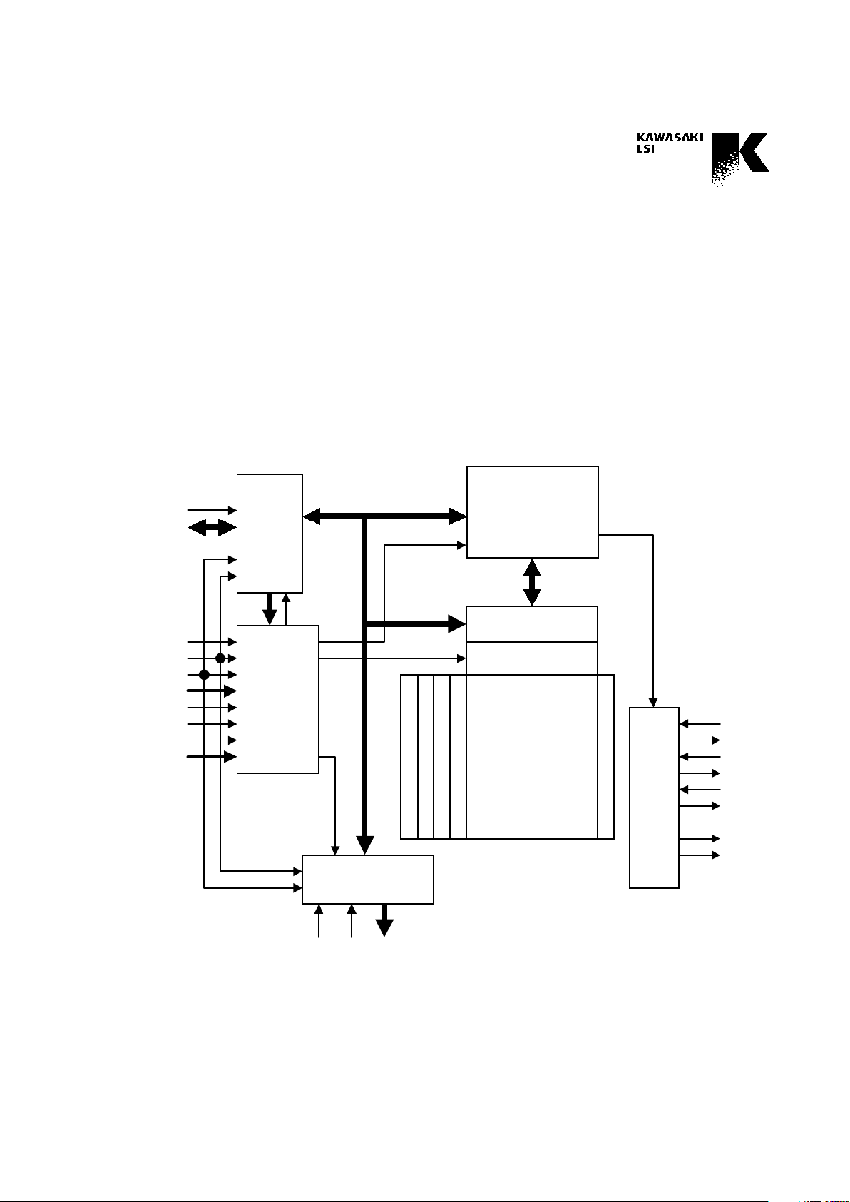
Fig. 2 Block Diagram
2. Block Diagram
This device consists of the following blocks as shown.
CPU Bus Control Block
An access to the search key data, commands, or internal regis-
ters are executed through the CPU Bus.
Pipeline Execution Control
This block controls the pipeline operation of this device.
CNTL1/2 Registers
These registers define the mask registers and the input
modes , etc.
Page 5

2-2
Preliminary
GigabitCAM KE5BGCA256
Memory R/W Registers
These registers are used to access the CAM table.
SCONF Register
This register defines the configuration of the search opera-
tion.
CMP1/2 Registers
These two registers store the search key data and both are
64 bits in width.
HHA/HEA Registers
These two registers respectively store the hit address and
the empty address of the CAM table.
MASK Registers
These 12 registers are used to mask the data bit by bit in
the search operation or the write operation to the CAM
table.
CAM
The capacity of the CAM table is 64 bits x 4096 entries.
Flag Logic
This block outputs the search result and the status of the
CAM table and has the interface function for a cascade
connection.
Output Port Control
This block controls the Output Port which outputs the
search result.
Page 6
3-1
Preliminary
GigabitCAM KE5BGCA256
38
39
1
128
103
65
64
102
Index
KE5BGCA256
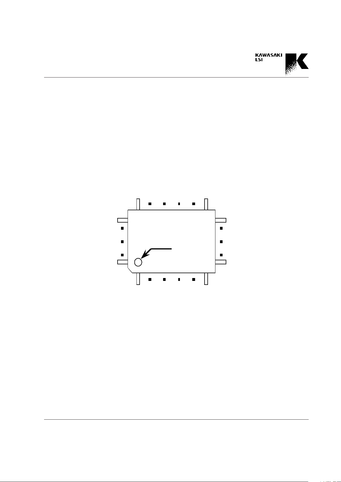
3. Pin Assignment and Pin Descriptions
3.1 Pin Assignment
KE5BGCA256
(128pin SQFP type)
Fig. 3.1.1 Pin Assignment
Page 7
3-2
Preliminary
GigabitCAM KE5BGCA256
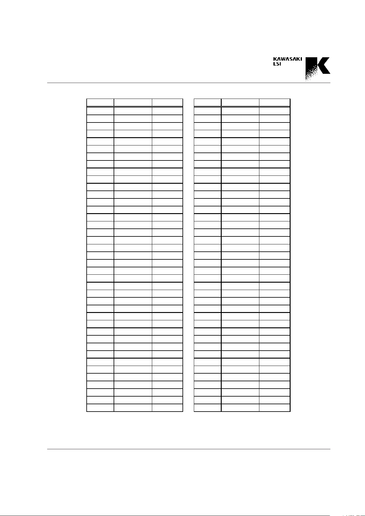
Pin No . Sign al Name I/ O typ e Pin No . Sign al Name I/ O typ e
1 GND - 41 GND 2 OD<0> OUT 42 PMON OUT
3 OD<1> OUT 43 PHON OUT
4VDD - 44FLININ
5VDD - 45PMININ
6 OD<2> OUT 46 PHIN IN
7 OD<3> OUT 47 VDD 8OD<4>OUT 48OPSL IN
9GND - 49OEODNIN
10 OD<5> OUT 50 GND 11 OD<6> OUT 51 GND 12 OD<7> OUT 52 GND 13 GND - 53 MS<0> IN
14 OD<8> OUT 54 MS<1> IN
15 VDD - 55 MS<2> IN
16 OD<9> OUT 56 MS<3> IN
17 OD<10> OUT 57 DAT<0> I/ O
18 GND - 58 DAT<1> I/O
19 GND - 59 VDD 20 GND - 60 DAT<2> I/O
21 OD<11> OUT 61 DAT<3> I/ O
22 VDD - 62 GND 23 OD<12> OUT 63 DAT<4> I/ O
24 VDD - 64 DAT<5> I/O
25 OD <13> OUT 65 GND 26 OD<14> OUT 66 DAT<6> I/ O
27 GND - 67 DAT<7> I/O
28 OD <15> OUT 68 VDD 29 OD <16> OUT 69 VDD 30 OD<17> OUT 70 DAT<8> I/ O
31 OD<18> OUT 71 DAT<9> I/ O
32 GND - 72 GND 33 OD<19> OUT 73 DAT<10> I/O
34 VDD - 74 DAT<11> I/O
35 VDD - 75 DAT<12> I/O
36 OD <20> OUT 76 GND 37 GND - 77 DAT<13> I/O
38 FLON OUT 78 VDD 39 SMON OUT 79 DAT<14> I/O
40 SHON OUT 80 VDD -
Table.3.1 Pin Assignment
Page 8
3-3
Preliminary
GigabitCAM KE5BGCA256
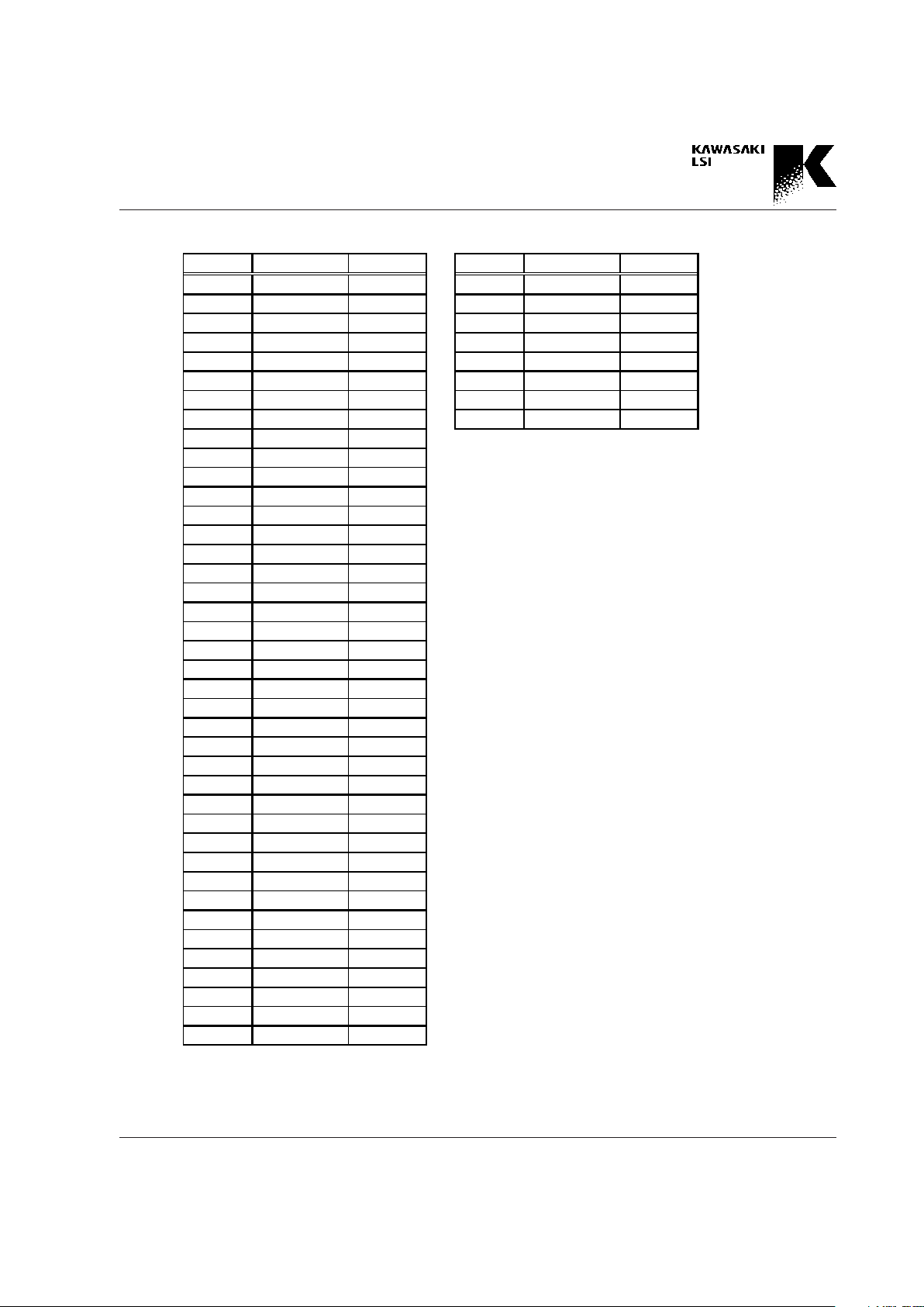
Pin No . Sign al Name I/ O typ e Pin No . Sign al Name I/ O typ e
81 PHA SE IN 121 CEN IN
82 CLK IN 122 RWN IN
83 GND - 123 SRCHN IN
84 GND - 124 OEDATN IN
85 GND - 125 NC OPEN*1
86 DAT<15> I/O 126 GND 87 DAT<16> I/O 127 GND 88 VDD - 128 GND 89 DAT<17> I/O
90 DAT<18> I/O *1 NC pins must be open. (Do not connect.)
91 DA T<19> I/O
92 GND 93 DA T<20> I/O
94 DA T<21> I/O
95 DA T<22> I/O
96 GND 97 DA T<23> I/O
98 VDD -
99 VDD 100 DAT <24> I /O
101 DAT <25> I /O
102 GND 103 DAT <26> I /O
104 DAT <27> I /O
105 GND 106 DAT <28> I /O
107 DAT <29> I /O
108 DAT <30> I /O
109 DAT <31> I /O
110 VDD 111 ADD<0> IN
112 ADD<1> IN
113 ADD<2> IN
114 ADD<3> IN
115 GND 116 GND 117 GND 118 ADD<4> IN
119 ADD<5> IN
120 RSTN IN
Table 3.1 Pin Assignment (cont'd)
Page 9

3-4
Preliminary
GigabitCAM KE5BGCA256
3.2 Pin Descriptions
Pi n name Attribute Functi on
CLK
CLOCK
Inp ut
LVTTL
CLK is the master clock input. Other input signals are referred to the
rising edge of CLK.
PHASE determines the action timing of the device. The latency of the
output is also determin ed by the relations hip between PHASE and
CLK.
PHA SE
PHASE
Inp ut
LVTTL
Regardless of whether the input mode is 32 bits (Normal Access
Mode) or 64 bits (First Access Mode), two cycles of the CLK signals
are necessary. PHASE regulates the input timing of the data input
from 32-b it DA T <31:0> when th e input mode is 64 b its .
When PHASE is high, the data on DAT<31:0> is input in the 32 bits
on th e MSB side of 64 bits. When PHASE is low,
the data is input in the 32 bits on the LSB side. When the input mode
is 32 bits, the 32-bit data is written in the register designated by
ADD<5:0> on the rising edge of CLK while PHASE is low.
DAT<3 1 :0 >
CPU Bu s
Input/Output
Tristate LVTTL
DATA<31:0> is a 32-bit, bidirectional data bus used to convey data,
to execute commands, and to write/read to and from the registers. The
direction is controlled by RWN and there is latency when the bus is
switched.
ADD<5:0 >
CPU Bus Address Bus
Inp ut
LVTTL
ADD<5:0> is a 6-bit address b us us ed to select registers.
CEN
Device Enable
Inp ut
LVTTL
CEN is used to access the CPU port. The active CEN enables the
inpu t operation of data and command.
RW N
Rea d/ Wr ite
Inp ut
LVTTL
RWN is u sed to determin e the direction of the CPU bus. RWN low
selects a write cycle, and RWN high selects a read cycle. There is
latency between the RWN change and the output as the result of the
data bus change.
OEDATN
CPU Bu s Output Enable
Inp ut
LVTTL
OEDATN c o ntro ls t he CPU b us ou tpu t. OEDATN low e n ables th e
output of the CPU bu s by the read operation, and OEDATN high
makes the CPU bus have high impedance despite the output
indication by the read operation. There is latency between the
OEDATN change and its result.
SRCHN
Search Enable
Inp ut
LVTTL
SRCHN enables the search operation together with the write
operation to the comparand register.
Page 10

3-5
Preliminary
GigabitCAM KE5BGCA256
Pi n name Attribute Functi on
MS <3 :0 >
Mask Select
Inp ut
LVTTL
MS<3:0> is a mask select signal. One of 12 Mask registers is selected
by th e M S<3:0>.
RS TN
Hardware Reset
Inp ut
LVTTL
RSTN is used to reset the hardware.
OD<20:0>
Output Port
Ou tp ut
Tristate LVTTL
OD<20:0> is a 21-bit output port. The device ID is output in the 5 bits,
OD<20:16> fro m t h e M SB, an d HHA, HEA , o r MEM HHA is outp ut in
the 16 bits from the LSB.
OEODN
Output Port Output Enable
Inp ut
LVTTL
OEODN c o n trols th e Outp ut Po rt. OEODN low enab les t h e ou t pu t,
and OEODN high disables the output (i.e. the Output Port is made
high impedance). There is latency between th e OEODN change and
its result.
OPSL
Output Port Select
Inp ut
LVTTL
OPSL low enables the output of MEMHHA from the Output Port.
There is latency between the OPSL change and its result.
SHON
Synchr onous Hi t Output
Ou t pu t
LVTTL
SHON outp uts the search results in the device synchronous with the
master clock. This p in is low when even one hit occurs in the search
operation. This pin is high when no entry is hit.
SMON
Synchr onous Multi-hit Ou tput
Ou t pu t
LVTTL
SMON outputs the s earch resu lts in the device synchronous with the
master clock. This pin is low when multi-hit occurs in the search
operation. This pin is high when no multi-hit occurs.
PHON
Priority Hit Output
Ou tpu t
LVTTL
PHON outputs the search results. This pin is not synchronous with
the master clock. This pin is low when even one hit occurs in the
search operation. This pin is high when no entry is hit.
In a cascaded system, the hit signal of the cascade configuration
appears in the PHON pin of the lowest priority device (Last Device).
PMON
Priority Multi-hit Output
Ou tp u t
LVTTL
PMON outputs the s earch resu lts. This pin is not synchronous with
the master clock. This pin is low when multi-hit occurs in the search
operation. This pin is high when no multi-hit occurs.
In a cascad ed system, the multi-hit signal of the cascade
configuration appears in the PMON pin o f the lowest p riority device
(Last Device).
Page 11

3-6
Preliminary
GigabitCAM KE5BGCA256
Pi n name Attri bute Function
PHIN
Priori ty Hit Input
Input
LVTTL
PHIN is used to connect plural devices in a cascaded system.
PMIN
Priority Multi-hit Input
Inp ut
LVTTL
PMIN is used to connect plural devices in a cascaded system.
FLO N
Full Flag Output
Ou tpu t
LVTTL
FLON outputs the search results. This pin is low when all entries in
the CAM are filled with valid entries (full status) and there is
no more entry for a new registration. In a cascaded system, the full
signal of the cascade configuration appears in the FLON pin of the
lowest priority device (Last Device).
FLIN
Full Flag Input
Input
LVTTL
FLIN is used in a cascaded system.
VD D S uppl y
Power s upply : 3.3V±0.3V
GND ( S uppl y) Gr o u n d
Ground
Page 12
4-1
Preliminary
GigabitCAM KE5BGCA256
4. Functional Descriptions
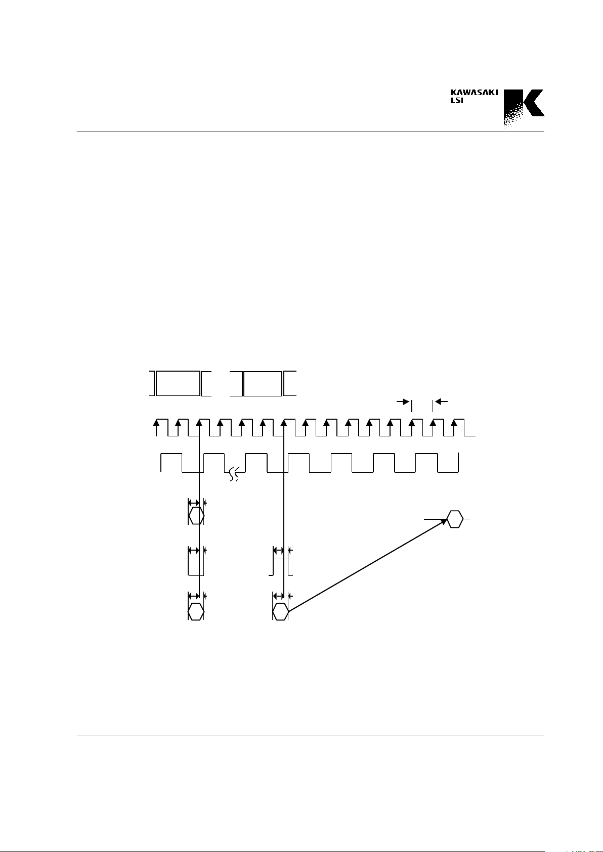
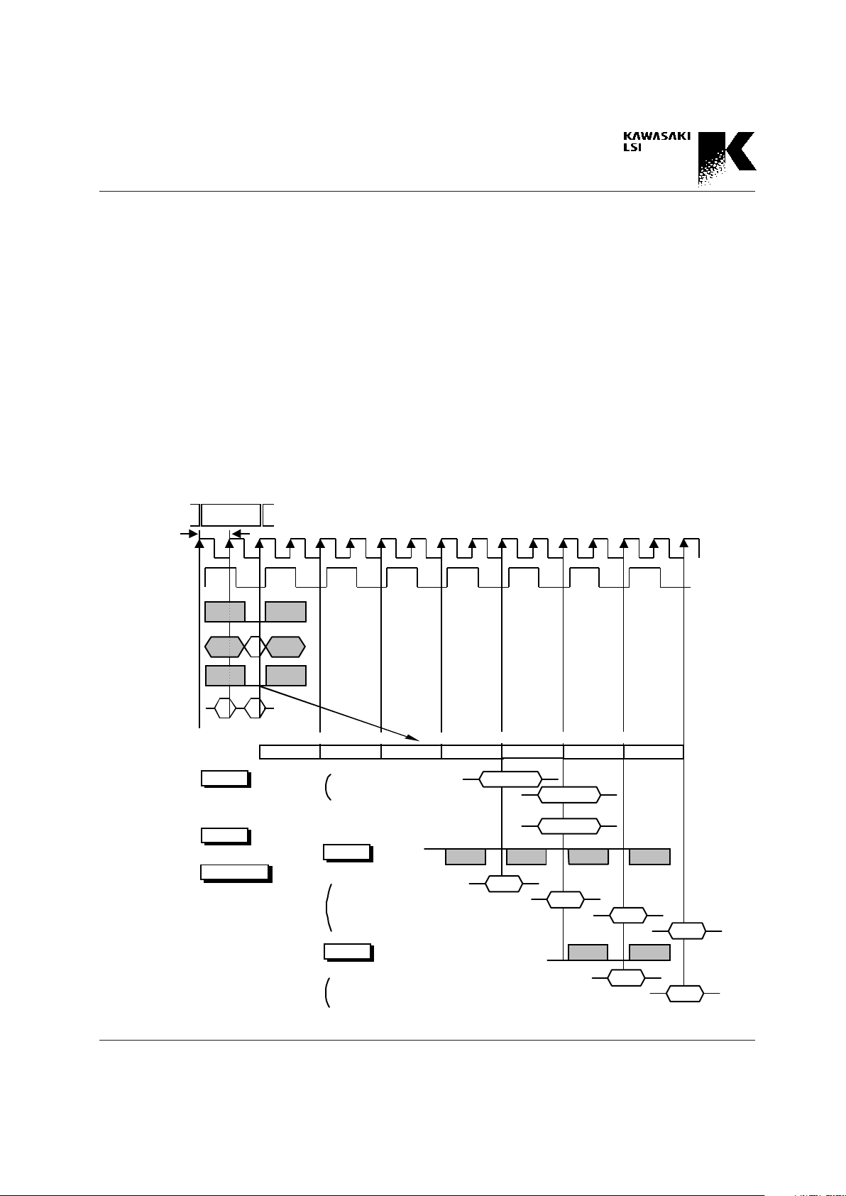
4.1 Access from CPU Port
This device has a 32-bit data bus as a CPU port. Data read/
write is performed by the registers that are mapped with 32-
bit width (Refer to Chapter 7.2). To access registers wider
than 32 bits or to access the CAM memory, two data read/
write accesses are required. A special high speed write
mode (Fast Write Mode) is provided for the data write.
Normal Access Mode
In this mode, one 32-bit data read/write is done with one
PHASE signal cycle. Data, address and control signals must
be input synchronously with the rising edge of CLK when
the PHASE signal, which is a double cycle signal of the
CLK, is low. (See Fig. 4.1.1 (a))
All the bits of each register address are valid in this mode.
Each 32-bit register is defined by the address pins
ADD<5:0>. Two accesses cycles are required for the read/
write of 64-bit registers and the CAM memory.
DAT<31:0>
CLK
PHASE
RWN
ADD<5: 0>, CEN
MS<3:0>, SRCHN
Setup Hold
Setup Hold
Setup Hold
Setup Hold
Setup Hold
Data write
(32bits)
Data read
(32bits)
Input
Operation
DAT rea d La tency=4
<63:32>
or
<31:0>
<63:32>
<31:0>
or
min. 15ns
Fig. 4.1.1 (a) CPU Access Mode (Normal Access Mode)
Page 13
4-2
Preliminary
GigabitCAM KE5BGCA256
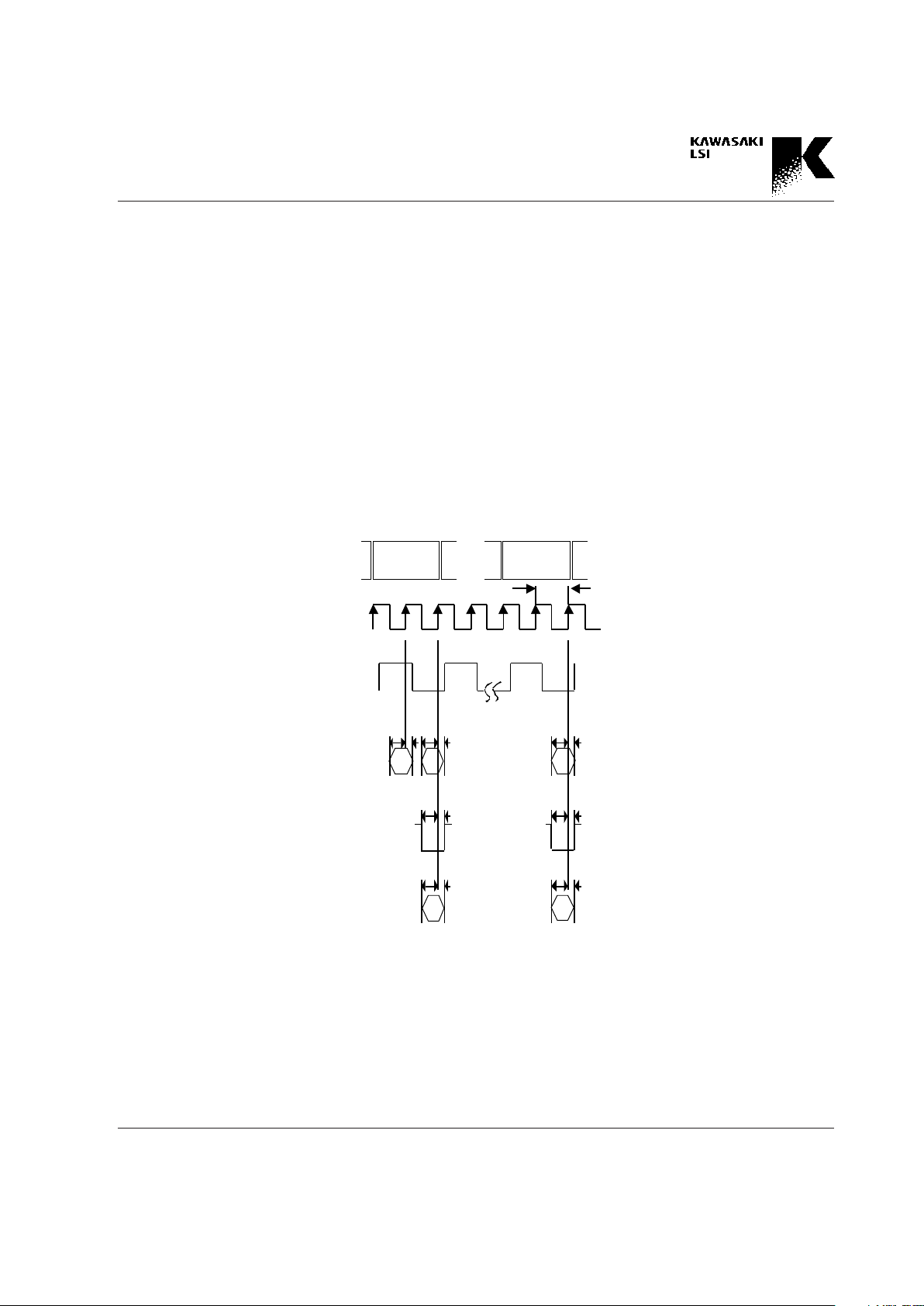
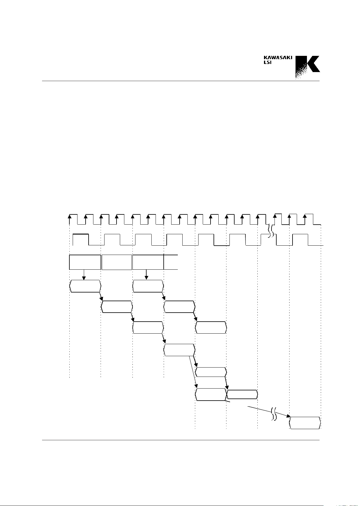
Fast Write Mode
In this mode, one 64-bit data read/write is done within one
PHASE signal cycle. The upper 32-bit data of the 64-bit reg-
ister is input synchronously with the rising edge of CLK
when the PHASE signal, which is a double cycle signal of
the CLK, is high. The lower 32-bit data of the 64-bit register,
address, and control signals are input synchronously with
the rising edge of the CLK signal when the PHASE signal is
low. (See Fig. 4.1.1 (b)) The LSB of the address is ignored in
this case. If a 32-bit register is accessed in this mode, only
the data, the address, and the control signals that are input
with the rising edge of CLK while the PHASE signal is low,
are valid. (See Fig. 4.1.1 (b)) The LSB of the address is also
ignored in this case.
Normal Access or Fast Write Mode is selected by the defi-
nition of the CNTL1 register. The initial definition after the
device reset is Normal Access Mode.
Fig. 4.1.1 (b) CPU Access Mode (Fast Write Mode)
CLK
PHASE
DAT< 31:0>
RWN
ADD<5:1>,CEN
MS<3:0>, SRCHN
Setup
Hold
Setup
Hold
Setup Hold
Setup
Hold
Setup Hold
Setup Hold
Data write
(64bits)
Data write
(32bits)
<63:32>
<31:0> <31:0>
min. 15ns
Operation
Input
Page 14
4-3
Preliminary
GigabitCAM KE5BGCA256
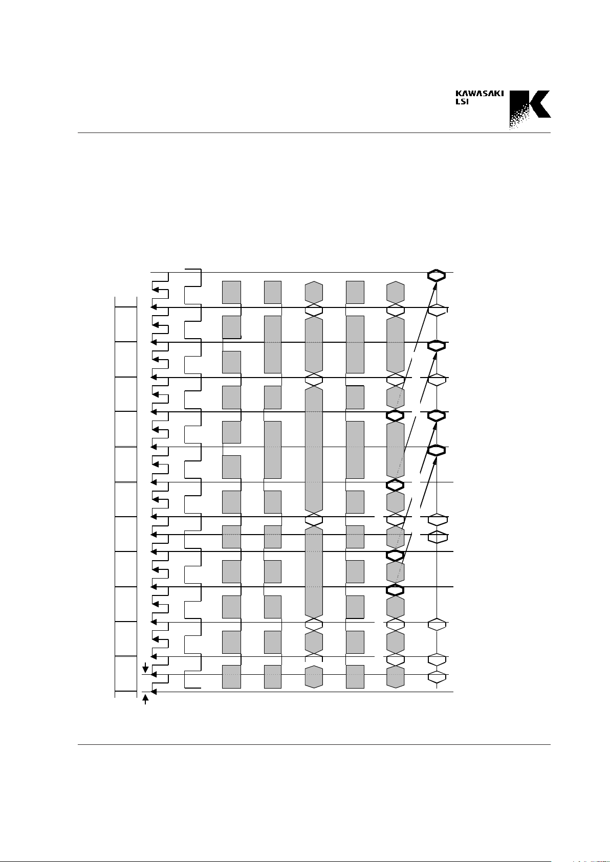
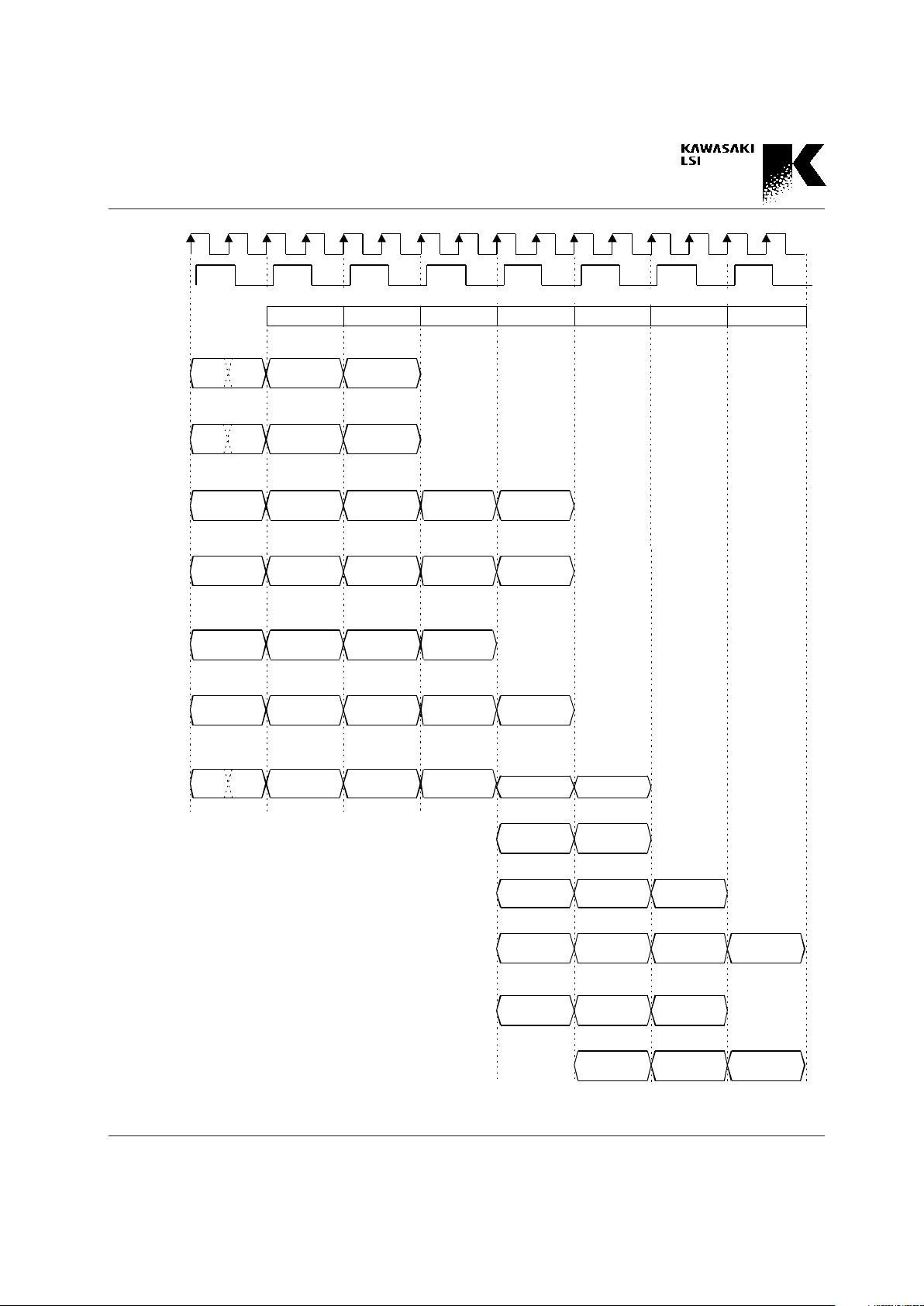
Fig. 4.2.1 Data read/write Timing Chart (Fast Write Mode)
4.2 Read/Write Registers
The register address is designated by the address pins of
the CPU port, and the data is inputted on the DAT bus. (See
Fig. 4.2.1) The function of each register is described in Chap-
ter 7. This figure shows the example of the Fast Write Mode.
In case of the Normal Access Mode, data write is the same
as the Fast Write Mode shown in Fig. 4.2.1 if you exclude
the write of the upper 32 bits of the 64-bit word.
CEN
CLK
PHASE
Data write
(64bits)
Input
Operation
RWN
MS< 3: 0>
SRCHN
ADD<5: 0>
DAT<31:0>
Data write
(32bits)
Data read
(32bits)
Data read
(32bits)
Data write
(64bits)
Data read
(32bits)
Data read
(32bits)
WAIT
Data write
(32bits)
Data write
(32bits)
WAIT
min. 15ns
<63:32><31:0>
<31:0> <31:0> <63:32>
or<31:0>
<63:32>
or<31:0>
<31:0> <63:32>
or<31:0>
<31:0>
<63:32>
or<31:0>
*1)64bits data write *1)
DAT read Latency=4DAT read Latency=4
<63:32>
Page 15

4-4
Preliminary
GigabitCAM KE5BGCA256
Fig.4.3.1 Word Structure of CAM
Permanent Bit
Access Bit
Empty Bit
Content
64 bits
1bit 1bit 1bit
4.3 Access to the CAM Memory
Word Structure of CAM
One word of the CAM is made up of 64-bit CAM memory
and 3 attribute bits (1 bit each). The 64-bit CAM memory
stores the users data to be searched. The attribute bits are
the Empty Bit, the Permanent Bit, and the Access Bit.
(See Fig. 4.3.1):
The Empty Bit: The Empty Bit is a flag that indicates the
validity of the CAM word. An invalid word is excluded from
the search target and is recognized as a candidate for
memory for a new registration of valid data.
The flag logic is:
0 : valid (Valid data is written);
1 : invalid (Memory is a space).
The Permanent Bit: The entry whose Permanent Bit is set
to "1" will not become invalid (Empty Bit = 1) by any purge
commands. In order to clear this bit, users can use the reset
command.
The Access Bit: The Access Bit is provided for the manage-
ment of the hit career of each entry. Users can specify
whether the hit career is held in the Access Bit or not for
each search cycle. Once the Access Bit is set to "1," how-
ever, it holds "1" until an Access Bit reset command is ex-
ecuted.
These attribute bits can be directly modified by accessing
the MEMAR_AT, MEMHHA_AT, and MEMHEA_AT
registers.
These bits are reset by the reset signal from the RSTN pin as
follows:
The Empty Bit : 1 (Invalid)
The Permanent Bit : 0 (Impermanent)
The Access Bit : 0 (No hit career)
Page 16

4-5
Preliminary
GigabitCAM KE5BGCA256
Read/Write CAM Memory
Read/write of the entry data is executed not by direct ad-
dress indication, but by indirect address indication through
specific registers (MEMAR, MEMARAI, MEMAR_AT,
MEMHHA, MEMHHA_AT, MEMHEA, MEMHEAAI, and
MEMHEA_AT). When writing through MEMAR,
MEMARAI, MEMHHA, MEMHEA, and MEMHEAAI, 12
kinds of mask conditions can be selected. Mask in the data
write operation means that the data of masked bit is not
changed by the write operation. There are two ways to se-
lect the mask condition from the 12 mask registers (MASK0
- MASK11). One way is to select it with 4 single pins,
MS<3:0> applied dynamically in data write. The other way
is to select by the definition in the CNTL1 register statically
.
The read/write of the CAM memory is basically the same as
the read/write of the registers. As shown in Fig. 4.2.1, the
mask condition in the write operation is selected by
MS<3:0>, the status of these select control signals is
latched by the rising edge of CLK while the PHASE signal is
low, and the data is written to the memory with Latency 2.
The read data is output from the CPU port with Latency 4.
(See Section 4.7 about Latency.)
Read/Write CAM Data through the MEMAR
register
Read/write operation of the CAM word, whose address is
designated by the AR register, is executed by the MEMAR
register. Write through the MEMAR register changes the
attribute bits in the CAM word as follows:
Empty Bit : 0 (Entry is valid.)
Permanent Bit : Return to the default value defined
in the CNTL1 register
Access Bit : Return to the default value defined in
the CNTL1 register.
Read/Write CAM Data through the
MEMARAI register
Read/write operation of the CAM word, whose address is
designated by the AR register, is executed by the
MEMARAI register. One read/write to the MEMARAI reg-
ister increments the value of the AR register automatically.
Write through the MEMARAI register changes the at-
tribute bits in the CAM word as follows:
Empty Bit : 0 (Entry is valid.)
Permanent Bit : Return to the default value defined
in the CNTL1 register.
Access Bit : Return to the default value defined in
the CNTL1 register.
Read/Write CAM Data through the
MEMHHA register
Read/write operation of the CAM word, whose address is
designated by the HHA register, is executed by the
MEMHHA register. Read/write through the MEMHHA
register is prohibited when the address stored in the HHA
register is invalid, because this may cause an access to the
undesired CAM word and the data in it might be destroyed.
Read/write through the MEMHHA register does not
change the attribute bits in the CAM word.
Page 17

4-6
Preliminary
GigabitCAM KE5BGCA256
Read/Write CAM Data through the
MEMHEA register
Read/write operation of the CAM word, whose address is
designated by the HEA register, is executed by the
MEMHEA register. Read/write through the MEMHEA reg-
ister is prohibited when the address stored in the HEA reg-
ister is invalid, because this may cause an access to the
undesired CAM word and the data in it might be destroyed.
Write through the MEMHEA register changes the attribute
bits in the CAM word as follows:
Empty Bit : 0 (Entry is valid.)
Permanent Bit : Return to the default value defined
in the CNTL1 register.
Access Bit : Return to the default value defined in
the CNTL1 register.
Read/Write CAM Data through the
MEMHEAAI register
Read/write operation of the CAM word, whose address is
designated by the HEA register, is executed by the
MEMHEAAI register. One read/write to the MEMHEAAI
register shifts the value of the HEA register to the value of
the next HEA automatically. Write through the
MEMHEAAI register changes the attribute bits in the CAM
word as follows:
Empty Bit : 0 (Entry is valid.)
Permanent Bit : Return to the default value defined
in the CNTL1 register.
Access Bit : Return to the default value defined in
the CNTL1 register.
Read/Write CAM Data through the
MEMAR_AT, MEMHHA_AT, and
MEMHEA_AT registers
Read/Write operation to the attribute bits of the CAM word,
whose address is designated by the AR, the HHA, and the
HEA registers respectively, is executed by these registers.
Examples of this operation would be to make the designated
CAM word Invalid, to make the designated CAM word Per-
manent, and/or to change the Access bit of the designated
CAM word. Users can mask each attribute bit. (Refer to
Chapter 7 for more details.)
This capability also enables the attribute of the CAM word
to be read.
Page 18
4-7
Preliminary
GigabitCAM KE5BGCA256
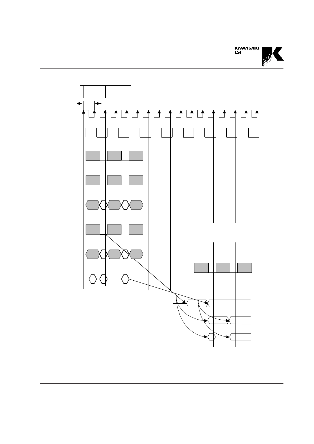
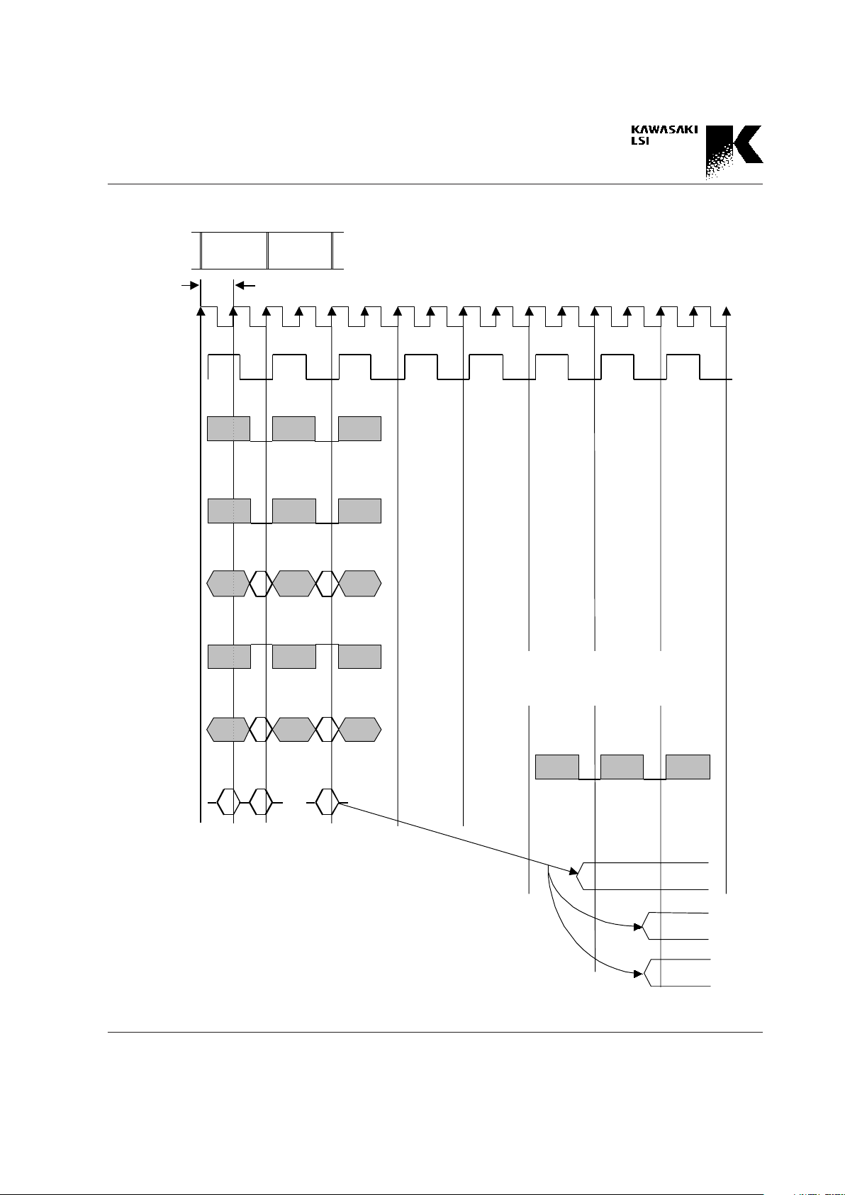
Fig. 4.4.1 SRCH Operation through CMP Register Write
4.4 Search
Search Operation through the CMP 1/2 regis-
ter
The key data should be written to the CMP1/2 register from
the CPU bus. The low pulse of the SRCHN pin synchro-
nized with the rising edge of CLK while the PHASE signal is
low activates the search operation when the key data is
written. The mask condition for the search is also chosen
from 12 kinds of mask conditions defined by the MASK
registers (MASK0 - MASK11), dynamically by the status of
the MS<3:0> pins or statically by the CNTL1 register.
The CMP1/2 register stores the key data until the next write
operation is done. Users can choose to perform a Search
Operation in the Normal Access mode or the Fast Write
mode. The example is shown in Fig. 4.4.1 (a/b).
In Fig. 4.4.1, the search operation is started by the data write
to the CMP1/2 register and the synchronous low pulse to
the SRCHN pin. As a result, the Hit flag is output on the
SHON pin with Latency 4, the Multi-Hit flag is output on the
SMON pin with Latency 5, and the HHA and the DEVID of
the device which has a hit are output on the OD<20:0> with
Latency 5. Fig. 4.4.1 shows two methods for searching the
CAM. In this example, the first search is executed by a
pulse from the SRCHN pin using the data previously written
to the CMP1/2 register. The second search operation is ex-
ecuted by the command, SRCH 1/2. This time, the search
operation by command is executed with the data already
written in the CMP1/2 register used in the previous search.
CEN
CLK
PHASE
SRCH
RWN
MS<3:0>
SRCHN
ADD<5:0>
DAT<31:0>
Data write
(32bits)
min. 15ns
<31:0>
(or<63:32>)
<63:32>
(or<31:0>)
SHON
SMON
OD<20:0>
<31:0>
COM
(SRCH)
(a) Normal Access Mode
Operation
Input
Latency
SHON: 4 (or 5)
SMON: 5
OD (HHA, DEVID): 5 (or 6, 7, 4)
OEODN
Page 19
4-8
Preliminary
GigabitCAM KE5BGCA256
Fig. 4.4.1 SRCH Operation through CMP Register Write
CEN
CLK
PHASE
RWN
MS< 3: 0 >
SRCHN
ADD<5: 1>
DAT<31:0>
SRCH
<31:0> <31:0><63:32>
COM
(SRCH)
(b) Fast Write Mode
Operation
Input
min. 15ns
SHON
SMON
OD<20:0>
Latency
SHON: 4 (or 5)
SMON: 5
OD (HHA, DEVID): 5 (or 6, 7, 4)
OEODN
Page 20
4-9
Preliminary
GigabitCAM KE5BGCA256
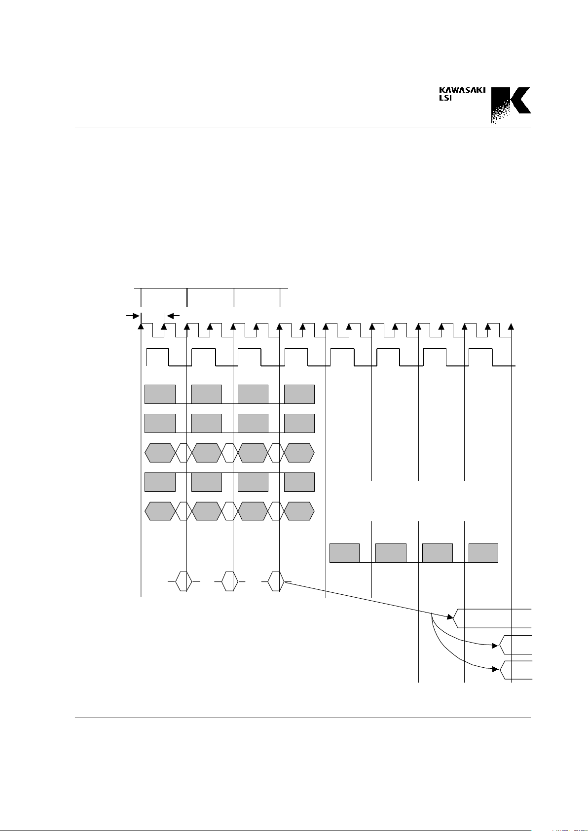
Fig. 4.4.2 SRCH Operation with COMMAND
Search Operation by commands
The search command, SRCH 1/2, written to the command
register (COM register) activates the search operation using
the key data stored in the CMP1/2 register.
The mask condition for the search is chosen at the time of
command write from 12 kinds of mask conditions defined by
the MASK registers (MASK0 - MASK11). The mask regis-
ter is chosen dynamically by the status of the MS<3:0> pins
on the rising edge of the CLK signal while the PHASE signal
is low or statically by the CNTL1 register. Like the search
operation above, users can choose the write mode from the
Normal Access mode or the Fast Write mode. In both
modes, the search operation is started by the command
(SRCH). The example is shown in Fig. 4.4.2 (a/b).
CEN
CLK
PHASE
Input
Operation
RWN
MS< 3: 0>
SRCHN
ADD<5: 0>
DAT<31:0>
Data write
(32bits)
m in. 15ns
<31:0>
(or<63:32>)
<63:32 >
(or<31:0>)
<31:0>
COM
(S RCH)
(a) Norm al Access Mode
Data write
(32bits)
SHON
SMON
OD<20:0>
Latency
SHON: 4 (or 5)
SMON: 5
OD (HHA, DEVID): 5 (or 6, 7, 4)
OEDON
Page 21
4-10
Preliminary
GigabitCAM KE5BGCA256
Fig. 4.4.2 SRCH Operation with COMMAND
CEN
CLK
PHASE
Input
Operation
RWN
MS< 3: 0>
SRCHN
ADD<5: 1>
DAT<31:0>
<31:0> <31:0><63:32>
SHON
SMON
OD<20:0>
COM
(S RCH)
(b) Fast Write Mode
Data write
(64bits)
m in. 15ns
OEODN
Latency
SHON: 4 (or 5)
SMON: 5
OD (HHA, DEVID): 5 (or 6, 7, 4)
Page 22

4-11
Preliminary
GigabitCAM KE5BGCA256
Access Bit set while searching
When a hit occurs in the CAM word while searching, the hit
result of the entry can be stored as the Access Bit data.
This means the past career of the hit results can be man-
aged. For every 12 MASK registers, the determination of
whether the search result is stored in the Access Bits or not
(whether the Access Bits must be set according to the hit
result) can be done using the SCONF register. (Refer to
Chapter 7 for more details.)
Search Result
Flag pins (PHON, PMON, SHON, SMON)
The PHON and SHON pins indicate if the Hit word (the
CAM word which is hit) exists. A high level on the PHON
pin indicates that a single hit does not exist and a low level
on this pin indicates that a single hit exists and multi-hit
does not exist. A high level on the SHON pin indicates that
no hit exist and a low level on this pin indicates that a single
hit or Multi-Hit exist. The PHON pin goes to an unknown
status when the search operation starts, and it outputs high
or low level according to the search result. The PHON pin
outputs the search results asynchronously with the CLK.
The SHON outputs the corresponding search result syn-
chronously with CLK. (See Fig. 4.4.2. Refer to Chapter 5 for
more details)
The PMON and SMON pins indicate if Multi-Hit entries
exist. A high level of these pins indicates that a multi-hit
does not exist and the low level of this pin indicates that a
multi-hit exists. The PMON and SMON pin goes to an un-
known status when the search operation starts, and it out-
puts high or low level according to the search result The
PMON pin outputs the search results asynchronously with
the CLK. The SHON outputs the corresponding search re-
sult synchronously with CLK. (See Fig. 4.4.2.)
HHA register
The HHA register stores the address of the CAM word that
is hit by the search operation. The HHA register has the
valid bit that indicates the validity of the data stored in the
HHA register. This valid bit becomes 0 if single hit (no
multi-hit word exist) exists. If a multi-hit or no hit exists, the
valid bit becomes 1 , invalid. The HHA register also
stores the data output to the PHON and PMON pins accord-
ing to the search result, namely Hit and Multi-Hit flag data
(Labeled SYH and SYM in section 7.3 Register Bit Maps). In
a cascaded system in which multiple devices are intercon-
nected, the Last Device in the chain holds the Hit and Multi-
Hit flags of the total system.
Careful consideration is required for the HHA register, be-
cause the HHA (Highest Hit Address) becomes invalid data
when a multi-hit exists. The search configuration register,
SCONF, allows the user to set the Access Bit according to
the search operation results. Even though a multi-hit is set
as invalid, all the Access Bits of Hit words are still set.
Hit and Multi-Hit status of the total system is valid only
when the HHA register in the Last Device is accessed with
the timing which considers the propagation delay between
the devices.
MEMHHA register
The MEMHHA register is used to read and write the hit
CAM. The mask condition in the 12 MASK registers is also
used for a partial write to modify part of the hit CAM word.
The write through the MEMHHA register is prohibited
when the address stored in the HHA register is invalid, be-
cause this may cause access to the undesired CAM word
and the data in it might be destroyed.
Page 23
4-12
Preliminary
GigabitCAM KE5BGCA256
Fig. 4.4.3 Output Port Format
OPSL = 1
20 16 15 14 1312 11 0
HHA or HEADEVID
HHA/HEA Fla
g
0: HHA
1: HEA
VALID Fla
g
0: Valid
1: Invalid
20 16 15
DEV IDOPSL = 0
0
Pa rt of MEMHHA
KE5BGCA256
OD<20:0>
Output from Output Port
The Output port is a 21-bit output bus used for the search
result. The main purpose of this port is to output the HHA.
Usually, 5 bits out of the 21 indicate the Device ID (the ID
data provided to recognize the device in the system with
multiple devices), and the other 16 bits output the HHA that
indicates the hit address in the device. The Output port is
controlled by the OEODN pin.
The HHA, the HEA, and part of the MEMHHA (16 bits) can
be output from the Output port. The SCONF register defines
which data set listed above will be output.
The SCONF register holds the following 5-bit information
for each of the 12 mask conditions. These bits determine
what kind of search result is output from the Output port,
caused by the corresponding mask condition:
AS* (1bit): Whether the Access Bits are set or not
HE* (1bit): Whether the HEA is output or not when no hit
MH* (1bit): Whether part of the MEMHHA is output or not
S*<1:0> (2bits): Which part of the MEMHHA is output
00: MEMHHA<15:0>, 01: MEMHHA <31:16>,
10: MEMHHA<47:32>, 11: MEMHHA<63:48>
(* : 00 - 11)
The output data selection with the OPSL pin is necessary to
output the MEMHHA. (See Fig. 4.4.3)
Page 24
4-13
Preliminary
GigabitCAM KE5BGCA256
Fig. 4.4.4 Output Latency of SRCH Operation
The latency (how many clock cycles of delay from the data
input) can be defined by the CNTL2 register. The latency of
the HHA output (or the HEA output) can be selected from 4,
5, 6 and 7. The latency of the MEMHHA output can be
selected from 6 and 7. (See Fig. 4.4.4)
If the Output port is connected to the same bus in a cas-
caded system, the output control with the OEODN pin or
with the latency selection is required so that the bus conflict
does not occur. (Refer to Chapter 5 for more details.)
Definition of the Mask Register for Search
and Write
KE5BGCA256 has 12 Mask registers. There are two meth-
ods of Mask selection for each of the four register groups.
One way is to select it dynamically with MS<3:0> pins. The
other way is to select it statically by the definition in the
CNTL1 register.
The registers are broken up into four groups as follows:
A Group: The search (or write) with the CMP1 or CMP2
register
B Group: The search with the SRCH1 command or the
SRCH2 command
CEN,
RWN
CLK
PHASE
Input
Operation
MS<3:0>,
ADD<5:0>
SRCHN
DAT<31:0>
SRCH
(a) Latency :4
<63:32>
SHON
SMON
OD<20:0>
Latency
min. 15ns
<31:0>
1
2 3 4
5 6 7
(b) Latency :5
Latency :5
MEMHHA
(a) Latency :6
(b) Latency :7
HHA(or HEA)& DEVID
(a) Latency :4
(b) Latency :5
(c) Latency :6
(d) Latency :7
OPSL
OPSL
Page 25

4-14
Preliminary
GigabitCAM KE5BGCA256
C Group: The write with the STR commands
D Group: The write with the MEM registers
Each of these groups has one bit in the CNTL1 register that
is used to define the method of selection, either from the pin
MS<3:0>, or from the register. If the mask condition is se-
lected from the register, there are four bits for each group in
the CNTL1 register that selects one of the 12 Mask regis-
ters. (Refer to Chapter 7 for more details.)
If the mask condition is defined to be selected by the pins,
following bits corresponds to each Mask register.
The data of MS<3:0> pins should be input synchronously
with the rising edge of CLK when the PHASE signal is low
level as described above.
MS<3:0> pins MASK register
0000 MASK 0 register defines the mask condition.
0001 MASK1 register defines the mask condition.
0010 MASK2 register defines the mask condition.
0011 MASK3 register defines the mask condition.
0100 MASK4 register defines the mask condition.
0101 MASK5 register defines the mask condition.
0110 MASK6 register defines the mask condition.
0111 MASK7 register defines the mask condition.
1000 MASK8 register defines the mask condition.
1001 MASK9 register defines the mask condition.
1010 MASK10 register defines the mask condition.
1011 MASK11 register defines the mask condition.
If the bit of the MASK register is 1, the bit is dont care
and not searched. If the bit of the MASK register is 0, the
bit is "care" and searched. One of the 12 MASK registers
must always be defined in the search operation.
MASK registers are also used for the mask condition of the
write operation to the CAM memory. If the mask is set (The
bit is 1.), the corresponding bit of the CAM memory is not
changed by the write operation. One of the 12 MASK regis-
ters must always be defined in the write operation.
4.5 Data Management by Commands
KE5BGCA256 has several commands for data management.
This chapter describes the important points. (Refer to Chap-
ter 6 for more details.)
Data management using Access Bits
The following three commands are provided regarding the
Access Bits:
PRG_AC: Erases all the CAM words whose Access Bits are
1.
PRG_NAC: Erases all the CAM words whose Access Bits
are 0.
RST_AC: Clears all the Access Bits (Access Bit: 0).
An example of using these commands would be to perform a
search with the definition that the hit career is being held in
the Access Bit, then delete unnecessary CAM words
whose Access Bits are 1 (or 0). Another example is to
delete all the CAM words which hit (or did not hit) after the
search with certain data.
Data management using Store Commands
STR1/2_HHA command
This command overwrites the data of the CMP1/2 register to
the hit CAM word using the mask condition of the defined
Mask register. In other words, this command is a partial
(maskable) write to the hit address, and it is useful for time
stamping to the CAM word. The time stamping data can be
used, for example, to find the oldest CAM words by search-
ing this, and delete them.
Page 26
4-15
Preliminary
GigabitCAM KE5BGCA256
Fig. 4.5.1 STR1/2_AUT Command Operation
CLK
PHASE
Input
Operation
Execute0
PinOut
HHA
Execute1
Output2
(OD)
PinOut
SRCH
SHON
Execute0: SRCH operation
Execute1: HHA output operation from the OD bus
SHON /S MON
Latency:5~7
Decode
& Setup
Operation
Request
(CPU)
STR 1/ 2
_AUT
Decode
& Setup
Operation
Request
(CPU)
Wait/Nop
Exe cute
WAIT
STR1/2_HEA command
This command overwrites the data of the CMP1/2 register
to the empty CAM word using the mask condition of the
defined Mask register. In other words, this command is a
partial (maskable) write to the empty address, and it is use-
ful to register new CAM word data when there is no hit
CAM word in the search.
The commands STR1/2_HHA and STR1/2_HEA should be
executed according to the search result. KE5BGCA256 op-
erates with the Pipeline method synchronously with the ex-
ternal system clock causing multiple steps of latency before
receiving the results of each operation. If the command is
executed after receiving the result of each operation, it will
affect the performance.
STR1/2_AUT command
To avoid the performance problem described above, the
STR1/2_AUT command is provided in this device.
This command executes the same operation as the STR1/
2_HHA command if the device has a hit, and executes the
Page 27

4-16
Preliminary
GigabitCAM KE5BGCA256
same operation as the STR1/2_HEA command if the device
does not have a hit. Users can execute this command re-
gardless of whether the device has a hit or not, so that the
overhead caused by the unnecessary judging cycles can be
reduced.
The example is shown in Fig. 4.5.1. The status of the internal
pipeline is also shown in the example. (Refer to Chapter 4.6
for more details.) The STR1/2_AUT command is executed
one wait after the external request for the search. The one
wait in this example is inserted because the idle time of one
PHASE signal is necessary to utilize the search result infor-
mation such as a Hit. However, the STR_AUT command
should only be used when the cascade connection uses
external logic. (Refer to Chapter 5 for more details.)
For these STR commands, users can use the mask condition
defined by MS<3:0> pins or the CNTL1 register. When
using the CNTL1 register, this would be group C.
4.6 Restriction in Pipeline Operation
KE5BGCA256 is designed to use a maximum main clock of
66 MHz. This clock is synchronized with external requests,
resulting in operations which are processed by the internal
Pipeline. Internal Pipeline processing has several stages
corresponding to various requests for operation. When us-
ers request multiple operations continuously from the out-
side, these operations must be requested so that a conflict
between the Pipeline stages does not occur.
This Chapter describes the ways the internal pipeline
stages work to process the external request, and the rules
for continuous input of the various operations.
Stages of pipeline
The following are five groups of stages of the Pipeline for
the operation request:
(1) Operation Request Stage
In this stage, the operation is requested through the CPU
bus, with the data and the address input being latched.
There are two kinds of stages, Read request stage and Write
request stage. The difference between these two stages de-
pends upon whether the DAT bus is occupied. The Read
request stage does not occupy the DAT bus, but the Write
request stage occupies the DAT bus.
(2) Decode & Setup Stage
This stage follows the Operation Request Stage. The data or
the address that is latched in the Operation Request Stage is
decoded to recognize the request, and then the necessary
data is set up in this stage.
(3) Execute Stage
In this stage, the external request for operation is executed.
There are two kinds of operations, the operations that can
be executed with the other pipeline stage, See Fig. 4.5.1, and
the operations that cannot be executed with the other pipe-
line stage, according to which block in the device is ex-
ecuted.
(4) Wait/Nop Stage
This stage is for the timing adjustment of the internal bus
driving.
(5) Output Stage
Two stages, Output1 and Output2, are included. Output1 is
the stage for the output of the DAT bus, and Output2 is the
stage for the output of the OD bus. Output1 and Output2
can be executed simultaneously because these ports, DAT
bus and OD bus, are different ports.
Processing and Pipeline Stages
The following seven Types are the categories of operation
according to the Pipeline Stages:
Page 28
4-17
Preliminary
GigabitCAM KE5BGCA256
Fig. 4.6.1(a) Pipeline Operation Stage Chart
PHASE
Latency
CLK
Decode
& Setup
Execute0 Wait/Nop
Execute2
Decode
& Setup
Execute
Decode
& Setup
Execute Execute
Decode
& Setup
Execute Wait/Nop
Output1
(CPU)
Decode
& Setup
Execute
Output1
(CPU)
PinOut
Output2
(OD)
SHON
HHA
Execute1
Output2
(OD)
SHON/SMON
HHA
Output2
(OD)
HHA
Output2
(OD)
Wait/Nop
1) with HHA output
2) with MEMHHA output
Output2
(OD)
a)
b)
c)
Wait/Nop
Wait/Nop
Wait/Nop
Wait/Nop
Wait/Nop
PinOut
Execute1
Execute1
Execute2
HHA Latency : 5
Decode
& Setup
Execute
Decode
& Setup
Execute Wait/Nop
Output1
(CPU)
Execute0: SRCH operation
Execute1: HHA output operation from the OD bus
Execute2: MEMHHA output operation from the OD bus
Operation
Request(CPU)
Operation
Request(CPU)
Operation
Request(CPU)
Operation
Request(CPU)
Operation
Request(CPU)
Operation
Request(CPU)
Operation
Request(CPU)
HHA Latency : 6
HHA Latency : 7
a)
b)
MEMHHA Latency : 6
MEMHHA Latency : 7
MEMHHA
MEMHHA
Type 7 : SRCH operation with HHA output
Type 1 : Register write operation
Type 3 : Reg ister (except HHA/HEA) read operation
Type 5 : 2-cycle com m a nd operation
Type 6 : HHA/HEA Register read operation
Type 2 : MEM write or 1-cycle comm and operation
Type 4 : MEM read opera tion
5 6 74
1
2
3
High Low
High Low
High Low
Page 29

4-18
Preliminary
GigabitCAM KE5BGCA256
Type1: Registers write operation
Type2: MEM* write operation *1 or 1 cycle
command operation
Type3: Registers (except HHA and HEA) read
operation
Type4: MEM* read operation *1
Type5: 2 -cycle command operation *2
Type6: HHA/HEA register read operation
Type7: SRCH operation with HHA read (with HEA
read)
*1): The read/write of the MEMHEAAI register is in
Type5.
*2): SRST, GEN_FL, NXT_HE, STR1_HEAAI,
STR1_AUTAI, STR2_HEAAI, STR2_AUTAI
commands
The Pipeline Stage timing of each Type is shown in Fig.
4.6.1. As shown in Fig. 4.6.1(a), the Operation Request Stage
in Type 1, 2, 7 is divided into two stages (High and Low)
because the 64-bit data could possibly be written to the
register or to the CAM word using the Fast Write Mode (64-
bit access per one PHASE signal cycle).
Restriction of simultaneous execution of
Pipeline Stages
There are some restrictions of simultaneous executions of
the internal Pipeline Stages. Basically, the simultaneous ex-
ecution of the different Pipeline Stages is possible if they are in
different Pipelines, but the simultaneous execution must meet the
following restrictions:
1) The Write Request of the Operation Request Stage and
the Output1 Stage must not be executed
simultaneously because they use the same bus (DAT
bus).
2) Any operation can execute simultaneously during
Wait/Nop Stages.
3) The possible simultaneous operations of the Execute
Stages between the multiple Pipelines are restricted to
the following 3 cases:
a) The Execute of Type5 and the Execute of Types 1- 7
b) The Execute of Type6 and the Execute of Types 1- 7
c) The Execute1 and the Execute2 of Type7 and the
Execute of Types 1- 6
These executions must follow the restriction shown in Table
4.6.1. The column of the Table 4.6.1 means Execute stage which is
possible to simultaneously execute. As shown in Fig. 4.6.1 (b),
the the column of the table means 1st Input Operation, and the
row of the table means 2nd Input Operation.
CLK
PHASE
Input
Operation
1st Input Operation 2nd Input Operation
Fig. 4.6.1(b) Restriction of pipeline
Page 30
4-19
Preliminary
GigabitCAM KE5BGCA256
with MEMHHA output
Type 1 :
Register write operation
Type 3 :
read operation
2-cycle command operation, MEMHEAAI
Type 6 :
HHA/HEA Register
read operation
Type 2 :
MEM_HHA, _HEA, _AR, _ARAI
write or 1-cycle command operation
Type 4 :
MEM_HHA, _HEA, _AR, _ARAI
with HHA output
with MEMHHA
output
Type 7 :
SRCH operation
Type 5 :
2-cycle command
operation *4)
Type 6 :
HHA/HEA Register
read operation
Type 7 :
SRCH operation with HHA output
*2)
*3) *3)
X
read operation
Register (except HHA/HEA)
Type 5:
1st Input
Operation
2nd Input
Operation
*1)
*5)
*6)
*6)
*1) Only the NXT_HE command and MEM write can be simultaneously executed.
*2) Impossible to simultaneously execute with the Execute 0 of the SRCH operation.
*3) Impossible to simultaneously execute with the write to the CNTL2 register.
*4) In case of the SRST command, reset operation has priority.
*5) Execute of the HEA read operation cannot be simult aneously executed Execute of
the GEN_FL, NXT_HE, STR1/2_HEAAI, STR1/2_AUTAI (mis-hit case), and MEMHEAAI access.
*6) Exe cute of the HHA rea d operat ion cannot be simultaneously executed Execute of search oper ation.
Table 4.6.1 Restriction of pipeline
: allowed
: allowed partially
: not allowed
X
X
X
X
X
X
X
X
X
Page 31

4-20
Preliminary
GigabitCAM KE5BGCA256
Fig.4.6.2 Restrictions between Data Read/Write Operations
Restriction in usage of the result of data
operation in each Pipeline
Data Write and Read
The write and read operations of the data are classified into
Type1/2 and Type3/4. As shown in Fig. 4.6.2, DATA
WRITE (2), (3) Input Operation can be put on after DATA
READ Input Operation to use pipeline of the device effectu-
ally. However, (4) ~ (5) Input Operation stage cannot be
used because data output of DATA READ (1) starts on the
WAIT stage (5).
Definition of Search Condition and Search
Operation
The search operation can executed immediately after the
search condition has been changed with the write to the
CNTL1 register , the MASK register, or to the SCONF regis-
ter. It is not possible to change the output latency during
the search operation. The search condition (latency) must
be kept unchanged until the Output operation of the search
result has been completed (See Fig. 4.6.4).
The output latency is defined in the CNTL2 register.
CLK
PHASE
Input
Operation
Execute
Decode
& Setup
DATA
WRITE
Execute
Decode
& Setup
Wait/Nop
Output1
(CPU)
Execute
Decode
& Setup
Operation
Request(CPU)
Operation
Request(CPU)
Operation
Request(CPU)
DATA
READ
DATA
WRITE
DATA
WRITE
Operation
Request(CPU)
Execute
& Setup
Decode
WAIT WAITWAIT
(1) (2) (3) (4) (5) (6)
Page 32

4-21
Preliminary
GigabitCAM KE5BGCA256
Search and Use of the Search Result
For continuous operations executed through the CPU, some
operations are restricted. These types of operations must
be executed according to the result of the previous opera-
tion. An example would be when reading the HHA through
the CPU port using the MEMHHA register after the search
operation. Using this example, the restriction of the usage of
the result of data processing is described. As shown in Fig.
4.6.1, the HHA is determined in the Wait/Nop Stage, one
cycle after the Execute0 stage for a search operation which
is Type7. If the reading of the MEMHHA is requested right
after the request of the search operation, as shown in Fig.
4.6.3 (a), the Execute of the read operation of the MEMHHA
is executed at the same time as the Wait/Nop stage of the
SRCH. The value in the HHA has not been decided yet, so
this Execute is not executed correctly. This is because the
reading operation of the MEMHHA uses the HHA. In the
cases as above, one wait is necessary before an operation
which uses the HHA, such as the request for reading the
MEMHHA register (See Fig. 4.6.3 (b).). If the search is per-
formed after an operation which uses the HHA, such as
reading the MEMHHA register, one wait is not necessary.
Change the HEA and Use of the HEA
In the same way as the HHA, two waits are necessary before
an operation which uses the HEA, such as the request for
reading the MEMHEA register (See Fig. 4.6.3 (c).).
If an operation which changes the HEA is performed after an
operation which uses the HEA, two waits are not necessary.
Operations which change the HHA or the HEA
and Operations which use the HHA or the HEA
The operations which change the HHA or change the HEA
and the operation which use the HHA or use the HEA, are
listed as follows.
Operations which change the HHA
Search operation with the SRCHN pin
SRCH1/2 command
Operations which change the HEA
MEMHEAAI register access
GEN_FL, NXT_HE, STR1/2_HEAAI, STR1/2_AUTAI
commands
Operations which use the HHA
MEMHHA register access
STR1/2_HHA, STR1/2_AUT (hit case),
STR1/2_AUTAI (hit case) commands
Operations which use the HEA
MEMHEA register access
MEMHEAAI register access
STR1/2_HEA, STR1/2_AUT (mis-hit case),
STR1/2_AUTAI (mis-hit case) commands
Page 33

4-22
Preliminary
GigabitCAM KE5BGCA256
Fig. 4.6.3(a) Restriction Example between Pipeline Operations
Decode
& Se tu p
Execute0
Wait/Nop
PinOut
HHA
Execute1
Output2
(OD)
SHON/ SMON
CLK
PHASE
PinOut
Decode
& Se tu p
Execute
Wait/Nop
Operation
Request(CPU)
Operation
Request(CPU)
Input
Operation
MEMHHA
read
SRCH
Decode
Execute0
Wait/Nop
PinOut
HHA
Execute1
Output2
(OD)
SHON/ SMON
PinOut
Operation
Request(CPU)
SRCH
Output1
(CPU)
SHON SHON
Execute0: SRCH operation
Exe cut e1: HHA out pu t op era ti on f ro m the OD bus
(1) (2) (3)
(a) Vi olation of Pipeli ne Operati ons
Execute (2) is executed ac cording
to HHA as the result of Exec ute( 1).
The Wait/Nop stage must be i n eff ect
f or the determination of HHA.
Page 34

4-23
Preliminary
GigabitCAM KE5BGCA256
Fig. 4.6.3 (b) Restriction Example between Pipeline Operations (cont'd)
Decode
& Set up
Execute0
Wait/Nop
PinOut
HHA
Execute1
Output2
(OD)
SHON/SMON
CLK
PHASE
PinOut
Decode
& Set up
Execute
Wait/Nop
Operation
Request(CPU)
Operation
Request(CPU)
Input
Operation
MEMHHA
READ
SRCH
Decode
& Set up
Execute0
Wait/Nop
PinOut
HHA
Execute1
Output2
(OD)
SHON/SMON
PinOut
Operation
Request(CPU)
SRCH
Output1
(CPU)
SHON SHON
Execute0: SR CH operation
Execut e1: HHA outpu t ope ratio n fro m t he OD bus
(1) (2) (3)
Execute (2 ) is executed accord ing
to HHA as the result of Execute(1) .
The Wai t/Nop st age must be in
ef fec t for th e determination of HHA.
Wait/Nop
Wait/Nop
Wait/Nop
Wait/Nop
WAIT
(b ) Appropriate Pi peline Operati ons
Page 35

4-24
Preliminary
GigabitCAM KE5BGCA256
Decode
& Setup
CLK
PHASE
Operation
Input(CPU)
Input
Operation
(1)
Wait/Nop
Wait/Nop
(c) Appropriate Pipeline Operations
Execute0: Renew the HEA operation
Operation
Decode
Execute
(2)
Output1
(CPU)
Wait/Nop
Wait/Nop
WAIT
Renew the HEA
operation
MEMHEA
WAIT
READ
Wait/Nop
Wait/NopExecute0 Execute0
Execute (2) is executed according
to HEA as the result of Execute(1).
The Wait/Nop stage m ust be in
eff ect for the d eterm ination of HEA.
Fig. 4.6.3 (c) Restriction Example between Pipeline Operations (cont'd)
Page 36

4-25
Preliminary
GigabitCAM KE5BGCA256
Fig. 4.6.4 Restrictions between SRCH Operation and Search Condition Definition Operation
Execute
CLK
PHASE
Operation
Request(CPU)
Input
Operation
REGISTER
WRITE
SRCH
Exe cute 0: SR CH operation
Execute2: MEMHHA output operation from the OD bus
Execute1: HHA output operation from the OD bus
Operation
Request(CPU)
Execute0
Decode
& Setup
Decode
& Setup
W ait/Nop
PinOut
HHA
Execute1
Output2
(OD)
PinOut
SHON
Decode
& Setup
Execute
Operation
Request(CPU)
CNTL2
WRITE
Execute2
ME MH H A
Output2
(OD)
SHON/SMON
Latency:4~7
Latency:6~7
Page 37

4-26
Preliminary
GigabitCAM KE5BGCA256
4.7 Latency
This device operates with the CLK signals as the master
clock. Therefore, there is latency which is characteristic for a
synchronous circuit between some action and the following
action. Latency is counted by the number of rising edge of
the CLK signals when the PHASE signal is low from the
input operation, as shown in Fig. 4.7.1, 4.7.2 For example,
Fig. 4.7.1 shows that the output latency of the CPU port is 4.
Fig. 4.7.2 shows that the output latency of the Output port
is 5.
Table 4.7.1 shows the output latency.
There is also execution latency in read/write operation by
commands or registers. (See Fig. 4.6.1)
The user that the values for latency can be modified by
writing to the CNTL2 register.
Fig. 4.7.1 Output Latency on the CPU Port
t1: output delay time from CLK
which is provided in Chapter 9
CLK
PHASE
CEN
D AT<3 1:0>
Register
Value
Latency = 4
t1
(1) (2 ) (3) (4)
Operation
Input
(5)
Count from this clock
OEDATN
Register
Read
Page 38

4-27
Preliminary
GigabitCAM KE5BGCA256
CLK
PHASE
CEN
OD<20:0>
Output
Latency =5
t1
Count from this clock
(1) (2) (3) (4)
Input
Operation
(5)
Operation
OEODN
Fig. 4.7.2 Output Latency on the Output Port
t1: output delay time from CLK
which is provided in Chapter 9
Table 4.7.1 Output Latency
Pins Latency
DA T<31:0>
· Latency is fixed to be 4.
· Lat ency (OEDATN => DAT<31:0>) is 1.
· Latency can be selected from 4, 5, 6, and 7 in HHA/HEA output.
OD<20:0>
· Latency from the operation to renew the HEA is equal to the HEA/HHA latency.
· Latency can be selected from 6 and 7 in MEMHHA output.
· Lat ency (OEODN => OD<20:0>) is 1.
· Latency can be selected from 4 and 5.
SHON · Latency is 2.5 when the SRST command is executed. (See Fig. 9.4.3)
· Latency is 0.5 from the RSTN low puls e. (See Fig. 9.4.3)
· Latency is fixed to be 5.
SMON · Latency is 2.5 when the SRST command is executed. (See Fig. 9.4.3)
· Latency is 0.5 from the RSTN low puls e. (See Fig . 9.4.3)
FLON
· When MEM_HEAAI is access ed or the GEN_FL, NXT_HE, STR1_HEAAI,
STR2_HEAAI, STR1_AUTAI, or STR2_AUTAI command is executed, latency is 2.5.
· Latency is 2 when the SRST command is executed.
· Latency is 0 from the RSTN low pulse.
PHON
· When the search operation by the SRCHN pin or the SRCH command is executed,
latency is 2.5.
· Latency is 0 from the RSTN low pulse.
PMON
· When the search operation by the SRCHN pin or the SRCH command is executed,
latency is 2.5.
· Latency is 0 from the RSTN low pulse.
· When the SRST, STR_DEVID, END_DEVID, and NXT_PR command is executed,
latency is 2.
Page 39

5-1
Preliminary
GigabitCAM KE5BGCA256
Normal Mode DEVID Mode
Power ON
Device Reset
STR_DEVID
command
END_DEVID
command
Fig 5.3.1.1 Device ID registration
5. Connection
5.1 Initialization
There are two types of initialization for this device: Hard-
ware reset by setting the RSTN pin to a low level, and Soft-
ware reset by executing the SRST command.
Hardware reset must be done after the power is on.
Hardware reset or Software reset executes the following ini-
tialization:
1) Initializes Device ID *1
2) Initializes registers
3) Sets Empty Bits of all entries (all entries are empty)
4) Clears Permanent Bits of all entries
5) Clears Access Bits of all entries
6) PHON = 1, SHON = 1
7) PMON = 1, SMON = 1
8) FLON = 1
*1 Device ID must be registered after reset when devices are
cascaded.
The GEN_FL command must be executed after registration
to the CAM table.
5.2 Single Device Operation
A device reset either by a Hardware reset using the RSTN
low pulse or software reset using the SRST command auto-
matically sets the Device ID to 00000 and the LD bit to 1.
The LD bit means the Last Device in a cascaded system.
Therefore, it is not necessary to set the Device ID by using
the DEVID mode in the single device operation. The PHIN
and PMIN pins must be pulled up and the FLIN pin must be
pulled down with a single device.
When used in a single device operation, the device acts as
one with hit/empty priority if there is any hit/empty entry in
the device. On the other hand, it acts as the Last Device if
there is no hit/empty entry in the device. Therefore, the be-
havior is the same in the broadcast method as in the device
select method, but some commands must be executed in the
device select method according to the condition of Table 6.2
, and some registers must be accessed in the device select
method according to the condition of Table 7.4.1, even in
this case.
Page 40

5-2
Preliminary
GigabitCAM KE5BGCA256
DEVICE ID
=0
DEVICE ID
=1
DEVICE ID
=2
DEVICE ID
=m
15 (LD)
0
000000
DEVIDL register
0
100000
31
0
010000
31
031
m(binary)
1
31
CLK
PHASE
ADD<5:0>
DAT<31:0>
CEN
RWN
COML DEVIDL
00000000H 00003000H
COML COMLDEVIDL
STR_DEVID
command
write to
DEVID register
NXT_PR
command
00000001H
write to DEVID
register
00003000H
.....
.....
DEVIDL
m
COML
00002800H
END_DEVID
command
DEVID mode
00000000H
NXT_PR
command
write to DEVID
register
15 (LD)
15 (LD)
15 (LD)
Fig.5.3.1.2 Device ID registration procedure
Page 41

5-3
Preliminary
GigabitCAM KE5BGCA256
5.3 Cascade Connection
5.3.1 Device ID Registration
The device can be cascaded to use a maximum of 32 devices.
A cascaded system can be treated as one device which has
a larger table size. It is necessary to define the Device ID in
the DEVID register in order to identify each device in the
operation of a cascaded system. The procedure for registra-
tion of the Device ID is shown in Fig. 5.3.1.2.
In order to set the Device ID, the devices in a cascaded
system must be moved into the DEVID mode by the
STR_DEVID command as shown in Fig. 5.3.1.1. The
STR_DEVID command enables the user to apply read/write
operations to the DEVID register of the highest (top) device
in the cascaded system. The Device ID is set in the DI<4:0>
of the register. After that, the Device ID of the next device
can be set by the NXT_PR command. The registration
should be repeated down the chain until each device is
given a unique Device ID by repeating these operations. If
the STR_DEVID command is executed among these opera-
tions, it returns to the status where the DEVID register of the
highest (top) device can be read/written.
The Device ID must be a continuous number starting from
the top device. The LD in the Last Device DEVID register
must be set to 1. This bit indicates that the device has the
lowest priority, and it is used to control the data outputs.
The LD bits of all devices except the Last Device must be set
to 0.
After the DEVID registers of all devices are set, the devices
should be moved out of the DEVID mode and into the nor-
mal operation mode by executing the END_DEVID com-
mand. The devices must leave the DEVID mode after all De-
vice IDs are set, because operations like Table Configura-
tion or search cannot be executed correctly in the DEVID
mode. Waiting time is recommended to ensure that the
PMIN and PMON pins become stable.
The Device IDs of all devices are initialized to the same
value of 00000 after device reset. The operations de-
scribed above, from the STR_DEVID command, must be ex-
ecuted after device reset. If only one device is used, the
Device ID registration is not necessary.
Do not register the Device ID in normal operation mode
once the Device ID is set after device reset.
5.3.2 Priority
In a cascaded system, the data buses of the CPU Port and
the Output Port must be connected to all devices. As for the
CPU Port, the same data is written to all devices through
DAT<31:0> and the same Pipeline is executed in all devices.
The output device is automatically determined in the broad-
cast method and the device in which the MEMHHA or the
MEMHEA register is written, or the device in which the
STR_HHA, the STR_HEA, or the STR_AUT command is
executed, is also determined automatically. As for the Out-
put Port, all devices output the search results respectively.
The Output Port must therefore be controlled by the users
logic using the SHON when there is a multi-hit in the system,
when there are many devices with a single hit, or when HEA
is set to be output in a no hit case.
The empty priority is controlled in this device, but the hit
priority is not controlled in order to realize a higher speed.
The HHA as a result of the multi-hit in the device therefore
becomes invalid, and the write operation to the entry desig-
nated by the HHA is not executed. The above-mentioned
priority control is, however, executed in the cascaded sys-
tem including the device in which the multi-hit occurs. It is
also possible not to write, regarding the multi-hit in the sys-
tem as illegal status by the cascade connection method de-
scribed later.
Page 42

5-4
Preliminary
GigabitCAM KE5BGCA256
KE5BGCA256
PHIN
PMIN
PHON
PMON
FLINFLON
CEN
RWN
CLK
SRCHN
PHASE
KE5BGCA256
PHIN
PMIN
PHON
PMON
FLINFLON
CEN
RWN
CLK
SRCHN
PHASE
KE5BGCA256
PHIN
PMIN
PHON
PMON
FLINFLON
CEN
RWN
CLK
SRCHN
PHASE
Multi Hit
Single Hit
Single Hit
PHON= L
PHON= H
PHON= L
PMON= L
PMON= L
PMON= L
FLON=L
FLON=H
FLON=H
No Single Hit Priority
No Empty Priority
Single Hit Priority
Empty Priority
No Single Hit Priority
No Empty Priority
No Empty Entr
y
Empty Entr
y
No Empty Entr
y
No W rite
No W rite
Data is written the HHA address
Fig.5.3.2.1 Cascade Connection
Page 43

5-5
Preliminary
GigabitCAM KE5BGCA256
Three priorities are used for these controls: the single-hit
priority, the empty priority, and the DEVID priority. THE
PHIN, PMIN, FLIN, PHON, PMON, and FLON pins are used
to propagate the priorities.
(1) Single Hit Priority
In a cascaded system, the uppermost located device among
all devices that have hit entries, except the devices in which
the multi-hit occurs, is defined as having hit priority. (See
Fig. 5.3.2.1) This priority is propagated through the PHON
and the PHIN. When a multi-hit does not occur in a device
and the upper devices have single hit priority, the PHON of
the device outputs 0. When neither single hit nor multi-hit
occurs in the device and the upper devices do not have
single hit priority, the PHON of the device outputs 1.
In order to have a device having single hit priority, the PHIN
of the device must be set to 1.
(2) Empty Priority
In a cascaded system, the uppermost located device among
all devices that have empty entries is defined as having
empty priority (See Fig.5.3.2.1). This priority is propagated
through the FLON and the FLIN. When a device is full sta-
tus and the upper devices are full, the FLON of the device
outputs 0. When the device is not full or the upper de-
vices are not full, the FLON of the device outputs 1. In
order to have a device having empty priority, the FLIN of the
device must be set to 0.
(3) DEVID Priority
DEVID priority specifies which device accepts the Device
ID data in the DEVID mode. DEVID priority is propagated
through the PMIN and PMON pins in the DEVID mode.
However, the PMIN and PMON pins propagate multi-hit in-
formation in something other than the DEVID mode.
(4) Last Device
The device located at the bottom of the cascaded chain
must be known in order to perform internal control of the
device. The LD bit in the DEVID register of the bottom de-
vice must be set to 1 to indicate that it is the Last De-
vice.
For example, the Last Device stores the total hit and empty
information of the cascaded system in the HHA and HEA
registers. The Last Device outputs the bits: HV, EV, SYH,
SYM, SYE, HT, MH, the address with hit priority or empty
priority when the HHA or HEA register is read in the broad-
cast method. If there is no device having single hit priority,
the Last Device outputs the data of the HHA register in the
broadcast method. The HV flag of the output data is 1 and
that indicates that the HHA is invalid. In the same manner, if
there is no device having empty priority, the Last Device
outputs the data of the HEA register in the broadcast
method. The EV flag of the output data is 1 and that indi-
cates that the HEA is invalid. In a cascade system, for regis-
ters that have the same data in each device, such as the
CNTL1/2 and the SCONF register, when these registers are
read in the broadcast method, the Last Device outputs the
registers data.
5.3.3 CPU Port in a Cascaded System
Read/Write Registers
Read/write operations (including command execution) can
be performed by both the broadcast and the device select
method.
This selection is defined in the DEVSEL register. The BR bit
in the DEVSEL register must be set to 0 in the device
select method The selected device can be specified by the
DS<4:0> in the DEVSEL register. The BR must be set to 1
Page 44

5-6
Preliminary
GigabitCAM KE5BGCA256
in the broadcast method. When data is written to a register,
one of the following operations is executed according to the
attribute of the register:
(1) Write to all devices simultaneously
(2) Write to the device which has single hit priority
(3) Write to the device which has empty priority
When data is read from a register, one of the following op-
erations is executed according to the attribute of the regis-
ter:
(1) Read from the Last Device
(2) Read from the device which has single hit priority
(3) Read from the device which has empty priority
For registers which must have common data for all devices,
the device select method is invalid and data is written to
appropriate register of all the devices. Some registers must
be accessed by the device select method. See Table 7.4.1 in
Chapter 7 for Read/Write availability of each register in the
broadcast method/device select method and the output de-
vice that is accessed in the broadcast method.
Command Execution
The command of the device should be executed by the
broadcast method in a cascaded system. The device to
which the command execution applies is automatically de-
cided internally in this case.
Cascade Connection of the CPU Port
Cascade connection methods of multiple devices are shown
below:
(1) Priority control without the external logic
(2) Priority control with the external logic
A cascade connection can be realized by either of the two
methods. Table 5.3.3.1 shows the relationship between cas-
cade input pins and their actions. When the priority is con-
trolled by the external logic, the external circuit must be de-
signed referring to Table 5.3.3.1 and Fig. 5.3.3.3.
(1) Connection without the External Logic
In this method, the external logic is not necessary to control
the priority (See Fig. 5.3.3.1). However, additional propaga-
tion time is needed according to the number of cascaded
devices. This is because the priority signal is cascaded
through each of the devices. We define two types of multi-
hits: When there are multiple hits within a single device, or
when there are two devices in a cascaded system that have
a single hit. When two devices have a single multi-hit, the
data is written in the HHA address of the uppermost single
hit priority device in the cascaded system. For devices that
have multiple hits within a single device, data will not be
written to the HHA address. Data will be written to the HHA
address in the next device in the cascade chain that has a
single hit priority. (See Fig. 5.3.2.1) The commands
STR1_AUT, STR2_AUT, STR1_AUTAI, and
STR2_AUTAI cannot be executed in this connection
method.
AC Characteristics in this method
This device can automatically perform its internal control
function by using respective priority signals. After the pri-
ority is changed by some action, the next operation which
needs priority determination must wait a certain time accord-
ing to the number of cascaded devices. As shown in Fig.
5.3.3.2, the total time between some action and the next op-
eration which needs priority determination is required for
priority determination.
t1: latency of the action in the top device
t2: delay time after latency of the action in the top device
Page 45

5-7
Preliminary
GigabitCAM KE5BGCA256
t3: propagation delay of priority signal from the top device
to the Last Device
t4: setup time for the action which needs priority determina-
tion in the Last Device
(2) Connection with the External Logic
In this method, external priority control logic is used to mini-
mize the cascade delay of the system (See Fig. 5.3.3.3). The
external control logic must generate the priority signal of
each device, PHIN. This is determined from the SHON pin,
which is output by each device in hit priority control. In the
case of writing to the MEM_HHA register or writing by the
STR1_HHA or the STR2_HHA command, the PHIN signal is
made with consideration of the writing timing in the device
as shown in Fig. 5.3.3.4. When the STR1_AUT or the
STR2_AUT command is used in a cascaded system, the
PHIN of each device must be controlled with consideration
of the action timing in each device as shown in Fig. 5.3.3.4.
AC Characteristics in this method
This device can automatically perform its internal control
function by using respective priority signals. After the pri-
ority is changed by some action, the next operation which
needs priority determination must wait a certain time accord-
ing to the number of cascaded devices. As shown in Fig.
5.3.3.4, the total time between some action and the next op-
eration which needs priority determination is required for
priority determination.
t1: latency of the action in each device
t2: delay time after latency of the action in each device
t3: propagation delay of priority signal from the external pri-
ority control circuit to each device
t4: setup time for the action which needs priority determina-
tion in each device
Page 46

5-8
Preliminary
GigabitCAM KE5BGCA256
Table 5.3.3.1 Operation by hit priority(in the broadcast method)
Operation by hit p riority (in the broadcast method)
Device external pin*1 Operation that needs Status in device Op eration
PMIN PHIN FLIN priority determination
X 0 X M EMH HA, Single hit No operation
X 0 X M EMH HA_AT(WRIT E) No hit No operation
X 0 X No hit No op eration
X 0 X M EM HHA, Single hit Hi-Z outp ut
X 0 X M EM HHA_AT (READ) M ulti-hit Hi-Z outp ut
X 0 X No hit Hi-Z outp ut
X 0 X HH A(READ) Single hit Hi-Z outp ut
X 0 X DA T<30,27,26,24>,<23:0> Multi-hit Hi-Z output
X 0 X *2 No hit Hi-Z outp ut
V
*3
0 X HH A(READ)
Single hit
Hi-Z outp ut or if the Last
Device, outp ut
V
*3
0 X DA T<31,29,28,25>
M ult i-hit
Hi-Z outp ut or if the Last
Device, outp ut
V
*3
0X*3
No hit
Hi-Z outp ut or if the Last
Device, outp ut
X 0 X STR1_HH A, STR2_H HA Single hit No op eration
X 0 X Multi-hit No operation
X 0 X No hit No op eration
X 0 X STR1_AU T, STR2_AUT Single hit No op eration
X 0 X Multi-hit No operation
X 0 X No hit No op eration
*1 "X" means "don't care."
*2 Each device drives DAT<30,27,26,24>,<23:0> in the 32-bit CPU Bus since this is resp ective information of each device.
*3 The Last Device drives DAT <31,29,28,25> in the 32-bit CP U Bus since this is information of t he cascaded system.
FLIN of the Last Device must be determined for t he SYE flag to be output exactly in DAT<25>.
PMIN of the Last Device must be determined for the SYM flag to be output exactly in DAT<28>.
Page 47

5-9
Preliminary
GigabitCAM KE5BGCA256
Table 5.3.3.1(cont'd)
Device external pin*1 Op eration Status in device Operation
PMIN PHIN FLIN
X 1 X MEMHHA, Single hit Write
X 1 X M EMH HA_AT(WRIT E) Multi-hit No operation
X 1 X No hit No op eration
X1X
MEMHHA,
MEMHHA_AT(READ) Single hit Output
X1X
M ult i- hit
Hi-Z outp ut or if the Last
Device, outp ut invalid data
X1X
No hit
Hi-Z outp ut or if the Last
Device, outp ut invalid data
X 1 X HH A(READ) Single hit Out p ut
X 1 X Bit< 30,27,26,24>,<23:0>
M ult i- hit
Hi-Z outp ut or if the Last
Device, outp ut invalid address
X1X*4
No hit
Hi-Z outp ut or if the Last
Device, outp ut invalid address
V
*5
1 X HH A(READ)
Single hit
Hi-Z outp ut or if the Last
Device, outp ut valid address
V
*5
1 X Bit< 31,29,28,25>
M ult i-hit
Hi-Z outp ut or if the Last
Device, outp ut valid address
V
*5
1X*5
No hit
Hi-Z outp ut or if the Last
Device, outp ut valid address
X 1 X STR1_HH A, STR2_H HA, Single hit*6 Write t o HHA*6
X 1 X Multi-hit*6 No op eration
X 1 X No hit*6 No operation
X 1 X STR1_AU T, STR2_AUT, Single hit*7 Write to HHA
X 1 X STR1_AU TAI, or ,STR2_AUTAI M ulti-hit*7 No operation
X10
No hit with empt y
ent ry *7
Write to HEA*8
X10
No hit without empty
ent ry *7
No operation
X11
No hit with empt y
ent ry *7
No operation
X11
No hit without empty
ent ry *7
No operation
*4 Each device drives DAT<30,27,26,24>,<23:0> in the 32-bit CPU Bus since this is resp ective information of each device.
*5 The Last Device drives DAT <31,29,28,25> in the 32-bit CP U Bus since this is information of t he cascaded system.
FLIN of the Last Device must be determined for t he SYE flag to be output exactly in DAT<25>.
PMIN of the Last Device must be determined for the SYM flag to be output exactly in DAT<28>.
*6 STR*_HHA is STR1_HHA or STR2_HHA . If the search result by the CMP1 register is a single hit, the STR1_HHA
command execut es t he w rit e op era t ion t hat t he dat a in t h e CM P1 regist er i s w rit ten in t he ent ry indicat e d by H HA1.
If the search result by the CM P2 register is a single hit, the STR2_H HA command executes the write op eration t hat the
data in the CMP2 register is written in the entry indicated by HHA2.
*7 STR*_AUT is STR1_AUT or STR2_AUT. If the search result by the CM P1 register is a single hit, the STR1_AUT
command executes the write operation that the data in the CM P1 register is written in the entry indicated by HHA1.
If there is no hit, write in the ent ry indicated by HEA1. If the search result by the CM P2 register is a single hit, the
ST R2_AUT command exec ut es the w rit e op erat ion t hat t he d at a in t he CM P2 re gist er i s writ t en in t he en t ry indicat ed
by HHA2. If there is no hit, write in the entry indicated by HEA2.
*8 If STR*_AU TAI is executed, renewal of the HEA address is performed simultaneously.
Page 48

5-10
Preliminary
GigabitCAM KE5BGCA256
Table 5.3.3.1(cont'd)
Operation by empty priority (in the broadcast method)
Device external pin*1 Op eration Status in device Operation
PMIN PHIN FLIN
XX0
MEMHEA,
MEMHEA_AT(WRITE) With emp ty entry Write*11
X X 0 or MEM HEAAI Without empty entry No operation
XX0
MEMHEA,
MEMHEA_AT(READ) With empt y entry Outp ut*11
X X 0 or MEM HEAAI Without empty entry
Hi-Z outp ut or if the Last
Device, outp ut invalid data
X X 0 HEA(READ) With empty entry Out p ut
X X 0 Bit<30,27,26,24>,<23:0>*9 Without empty entry
Hi-Z outp ut or if the Last
Device, outp ut invalid address
V
*10V*10
0 HEA(READ) With emp ty entry
Hi-Z outp ut or if the Last
Device, outp ut valid address
V
*10V*10
0 Bit<31,29,28,25>*10 Without emp ty entry
Hi-Z outp ut or if the Last
Device, outp ut valid address
X X 0 STR1_HEA, STR2_HEA, With emp ty entry Write*12
X X 0 STR1_HEAAI, or STR2_HEAAI Without emp ty entry No operation
X
X1
MEMHEA,
MEMHEA_AT(WRITE)
With emp ty entry
No operation
X X 1 or MEM HEAAI Without empty entry No operation
XX1
MEMHEA,
MEMHEA_AT(READ) With empt y entry Hi-Z
X X 1 or MEM HEAAI Without empty entry Hi-Z
X X 1 HEA(READ) With empty entry Hi-Z
X X 1 Bit<30,27,26,24>,<23:0> Without emp ty entry Hi-Z
X X 1 HEA(READ) With emp ty entry
Hi-Z outp ut or if the Last
Device, outp ut valid address
X X 1 Bit<31,29,28,25> Without empty entry
Hi-Z outp ut or if the Last
Device, outp ut valid address
X X 1 STR1_HEA, STR2_HEA, With emp ty entry No operation
X X 1 STR1_HEAAI, or STR2_HEAAI Without emp ty entry No operation
*9 Each device drives DAT<30,27,26,24>,<23:0> in the 32-bit CPU Bus since this is resp ective information of each device.
*10 The Last Device drives DAT <31,29,28,25> in the 32-bit CP U Bus since this is information of t he cascaded system.
PMIN of the Last Device must be determined for the SYM flag to be output exactly in DAT<28>.
PHIN of the Last Device must be determined for t he SYH flag to be output exactly in DAT <29>.
*11 If the MEMHEAAI register is accessed, renewal of the HEA address is performed simultaneously.
*12 If the STR1_HEAA I or the STR2_HEAAI command is executed, renewal of the HEA address is performed
simultaneously.
Page 49

5-11
Preliminary
GigabitCAM KE5BGCA256
Table 5.3.3.1(cont'd)
Operation by hit priority (in the device select method).
In devices t hat are not s elected, no operation is performed for write group op eration, and Hi-Z outp ut is performed
for read group op eration.
Device external pin*1 Op eration Status in device Operation
PMIN PHIN FLIN
X X X MEMHHA, Single hit Write
X X X M EMH HA_AT(WRIT E) Multi-hit No operation
X X X No hit No op eration
X X X M EM HHA, Single hit Out p ut
X X X M EM HHA_AT (READ) M ulti-hit Outp ut invalid data
X X X No hit Out p ut invalid data
X X X HH A(READ) Single hit Out p ut
X X X Bit< 30,27,26,24>,<23:0>*13 Multi-hit Outp ut invalid address
X X X No hit Outp ut invalid address
X X X HH A(READ) Single hit Out p ut
X X X Bit< 31,29,28,25>*14 Multi-hit Outp ut
X X X No hit Out p ut
X X X STR1_HH A or STR2_HHA Single hit*15 Write
X X X Multi-hit*15 No operation
X X X No hit*15 No operation
X X X STR1_AU T, STR2_AUT, Single hit*16 Write to HHA*16
X X X STR1_AU TAI, or ,STR2_AUTAI M ulti-hit*16 No operation
X X X No hit*16 Write to HEA*16,17
*13 Each device drives DAT<30,27,26,24>,<23:0> in the 32-bit CPU Bus since this is resp ective information of each device.
*14 The Last Device drives DAT <31,29,28,25> in the 32-bit CP U Bus since this is information of t he cascaded system.
*15 STR*_H HA is STR1_HH A or STR2_HHA. If the search result by CM P1 is a single hit, the STR1_HHA command
execut es t he w rit e op era t ion t hat t he dat a in t he CM P1 regist er i s w rit ten in t he ent ry indicat e d by HHA1. If t he s earch
result by CM P2 is a single hit, the STR2_HHA command executes the write operation that the data in the CMP2
register is written in the entry indicated by HHA2.
*16 STR*_AUT is STR1_AUT or STR2_AUT. If the search result by CM P1 is a single hit, the STR1_A UT command
execut es t he w rit e op era t ion t hat t he dat a in t he CM P1 regist er i s w rit ten in t he ent ry indicat e d by HHA1. If t here is no
hit, write in t he entry indicated by HEA1. If the search result by CM P2 is a single hit, the STR2_AUT command
execut es t he w rit e op era t ion t hat t he dat a in t he CM P2 regist er i s w rit ten in t he ent ry indicat e d by HHA2. If t here is no
hit, write in t he entry indicated by HEA2.
*17 If the STR1_AUTAI or the STR2_A UTAI command is executed, renewal of the H EA address is p erformed
simult aneously .
Page 50

5-12
Preliminary
GigabitCAM KE5BGCA256
Table 5.3.3.1(cont'd)
Operation by empty priority (in the device select method)
In devices t hat are not s elected, no operation is performed for write group op eration, and Hi-Z outp ut is performed
for read group operation.
Device external pin*1
Op era t ion
Status in device
Op era t ion
PM IN
PHIN
FLINXXXMEMHEA(WRITE)
With emp ty entry
Write*20
XXX
or MEMHEA_AT
Without empty entry
No operation
XXX
MEMHEA,
With emp ty entry
Outp ut*20
XXX
or MEMHEAAI_AT(READ)
Without empty entry
Outp ut invalid data
XXX
HEA(READ)
With emp ty entry
Outp ut
XXX
Bit<30,27,26,24>,< 23:0>*18
Without empty entry
Outp ut invalid address
XXX
HEA(READ)
With emp ty entry
Outp ut
XXX
Bit<31,29,28,25>*19
Without empty entry
Outp ut
XXX
STR1_HEA, STR2_HEA
With emp ty entry
Write*21
XXX
or STR1_HEAAI, STR2_HEAAI
Without empty entry
No operation
*18 Each device drives DAT<30,27,26,24>,<23:0> in the 32-bit CPU Bus since this is resp ective information of each device.
*19 The Last Device drives DAT <31,29,28,25> in the 32-bit CP U Bus since this is information of t he cascaded system.
*20 If the MEMHEAAI register is accessed, renewal of the HEA address is performed simultaneously.
*21 If the STR1_HEAA I or the STR2_HEAAI command is executed, renewal of the HEA address is performed
simultaneously.
Page 51

5-13
Preliminary
GigabitCAM KE5BGCA256
Fig. 5.3.3.1 Simple cascade connection
KE5BGCA256
PHIN
PMIN
PHON
PMON
FLINFLON
CEN
RWN
CLK
SRCHN
PHASE
KE5BGCA256
PHIN
PMIN
PHON
PMON
FLINFLON
CEN
RWN
CLK
SRCHN
PHASE
KE5BGCA256
PHIN
PMIN
PHON
PMON
FLINFLON
CEN
RWN
CLK
SRCHN
PHASE
Page 52

5-14
Preliminary
GigabitCAM KE5BGCA256
Operation1
CLK
PHASE
CEN
t1 + t2 *1
Valid
Operation2
Valid
t3
t4
3 clocks *2
Valid
5 clocks *3
t3 t4
Operation which changes priority
Operatio n which needs prio rity
determination
PHIN, PMIN, FLIN
of the last device
PHIN, PMIN, FLIN
of the last device
Start command or
register access
PHON , PMON, FLON
of the top device
signal propagation
Fig. 5.3.3.2 Priority decision timing in a cascaded system (Simple cascade connection)
*1 When the operation which changes the priority falls
under one of the cases shown below, t1 is Latency 1.5 (= 3
clock).
1) Search by the SRCHN pin
2) Search by the SRCH command
3) Execution of the MEMHEAAI(Read/Write),
NXT_HEA, GEN_FL, or STR1_HEAAI/
STR2_HEAAI command
When the operation which changes the priority falls
under reset by the SRST command, t1 is Latency 1 (= 2
clock).
When the operation which changes the priority falls
under reset by the RSTN pulse, t1 is Latency 0 (= 0 clock).
t2 is the same in any case shown above.
*2 If the operation which needs priority determination
falls under one of the cases shown below, the setup time is
counted from 3 clock after input of the operation.
1) Execution of the MEMHHA(Read/Write),
MEMHEA(Read/Write), MEMHEAAI(Read/
Write), STR1_HHA/STR2_HHA, STR1_HEA/
STR2_HEA, or STR1_HEAAI/STR2_HEAAI
command
*3 If the operation which needs priority determination is
HHA(Read) or HEA(Read), the setup time is counted from
5 clock after input of the operation.
Page 53

5-15
Preliminary
GigabitCAM KE5BGCA256
To external Priority
Control logic
From external logic
From external logic
External
Priorit
y
Control Logic
SHON0
SHONn
FLON0
FLONn
PHIN0
PHINn
FLIN2
FLINn
From external logic
CLK
To external Priority
Control logic
To external Priority
Control logic
PHASE
PMIN2
PMINn
PMON0
PMONn
*1 PHIN and PMON are use
d
to propagate device priority an
d
multi-hit flag.
KE5BGCA256
PHIN
PMIN
PHON
PMON
FLINFLON
SHON
SMON
OEODN
CEN
RWN
CLK
SRCHN
PHASE
KE5BGCA256
PHIN
PMIN
PHON
PMON
FLINFLON
SHON
SMON
OEODN
CEN
RWN
CLK
SRCHN
PHASE
KE5BGCA256
PHIN
PMIN
PHON
PMON
FLINFLON
SHON
SMON
OEODN
CEN
RWN
CLK
SRCHN
PHASE
Fig.5.3.3.3 Cascaded system with external priority control logic example
Page 54

5-16
Preliminary
GigabitCAM KE5BGCA256
Operation1
CLK
PHASE
CEN
t1 + t2 *1
Valid
Operation2
Valid
t3 t4
3 clocks *2
Valid
5 clocks *3
t3 t4
Valid
t5 + t6 *4
Start command or
register access
Operation which changes the priority
Operation which needs priority
determination
PHIN, PMIN, FLIN
of each device
PHIN, PMIN, FLIN
of each device
signal propagation
PHON , PMON, FLON
of each device
SHON (Latency=4)
of each device
*1 When the operation which changes the priority falls
under one of the cases shown below, t1 is Latency 1.5 (= 3
clock).
1) Search by the SRCHN pin
2) Search by the SRCH command
3) Execution of the MEMHEAAI(Read/Write),
NXT_HEA, GEN_FL, STR1_HEAAI/
STR2_HEAAI, or STR1_AUTAI /
STR2_AUTAI command
When the operation which changes the priority falls
under reset by the SRST command, t1 is Latency 1 (= 2
clock).
When the operation which changes the priority falls
under reset by the RSTN pulse, t1 is Latency 0 (= 0 clock).
t2 is the same in any case shown above.
*2 If the operation which needs priority determination falls
under one of the cases shown below, the setup time is
counted from 3 clock after input of the operation.
1) Execution of the MEMHHA(Read/Write),
MEMHEA(Read/Write), MEMHEAAI(Read/
Write), STR1_HHA/STR2_HHA, STR1_HEA/
STR2_HEA, STR1_HEAAI/STR2_HEAAI,
STR1_AUT/STR2_AUT, or STR1_AUTAI/
STR2_AUTAI
*3 If the operation which needs priority determination is
HHA(Read) or HEA(Read), the setup time is counted
from 5 clock after input of the operation.
*4 In Fig. 5.3.3.4, the latency of the SHON of each device
is 4. Therefore, t5 is latency 4 (= 8 clock) and t6 is delay
time.
Fig.5.3.3.4 Priority decision timing in a cascaded system with external priority control logic
Page 55

5-17
Preliminary
GigabitCAM KE5BGCA256
Table 5.3.3.2 Relations between the operation which changes the priority and the operation which needs priority
determination
*1 Output variations of PHON, PMON, SHON, and SMON are shown below.
PHON
Output
PHIN PMIN Status in the device
Low 0 Don't care Single hit only
Low 0 Don't care Multi-hit
Low 0 Don't care Others
Low 1 Don't care Single hit only
High 1 Don't care Multi-hit
High 1 Don't care
Others
Operation1 Operation2
Operation which changes the priority Operation which needs priority determination
Single hit the priority propagation
Pins whose s tatus
changes
Command Pin s t o
consider
Search by the SRCHN pin PHON, PMON, MEMHHA(Read/Write) PHIN
command SHON, SMON *1 MEMHHA_ AT(Read/W rite) PHIN
Search by the SRCH command PHON, PMON,
HHA(Read)
PHIN
command SHON, SMON *1 STR1_HHA command PHIN
Reset by the SRST command PHON, PMON, STR2_HHA command PHIN
command
SHON, SM ON *1 STR1_ A UT comman d
STR2_AUT command
PHIN, PFIN
Reset by the RSTN puls e PHON, PMON,
SHON, SM ON *1
STR1_AUTAI command
STR2_AUTAI command
PHIN, PFIN
Empty priority propagation
Pins whose s tatus
changes
Command Pin s t o
consider
MEMHEAAI(Read/Write) PFON MEMHEA(Read/Write) FLIN
command command MEMHEA_AT(Read/Write) FLIN
NXT_HEA command FLON *2 MEMHAEAAI(Read/Write) FLIN
GEN_FL command HEA(Read) FLIN
STR1_HEAAI command
STR2_HEAAI command
FLON *2 STR1_ HEA co mmand
STR2_HEA command
FLIN
STR1_AUTAI command (in no hit)
STR2_AUTAI command (in no hit)
FLON *2 STR1_ HEAAI c o mmand
STR2_HEAAI command
FLIN
Reset by the SRST command FLON *2 STR1_AUT command
STR2_AUT command
PHIN, FLIN
Reset by the RSTN pulse FLON *2 STR1_AUTAI command
STR2_AUTAI command
PHIN, FLIN
Page 56

5-18
Preliminary
GigabitCAM KE5BGCA256
PMON
Output
PHIN PMIN Status in the device
Low 0 0 Single hit only
Low 0 0 Mu lti -hi t
Low 0 0 Oth er s
Low
01
Single hit only
Low 0 1 Mu lt i- hi t
High 0 1 Oth ers
Low 1 0 Single hit only
Low 1 0 Mu lti -hi t
Low 1 0 Oth er s
High 1 1 Single hit only
Low 1 1 M u lt i- h it
High 1 1 Oth ers
SHON
Outp ut
PHIN Status in the device
Low Don't care
Single hit only
High Don't care Others
SMON
Output
PHIN
Status in the device
Low Don't care Mu lti-hit
High Don't care Others
Table 5.3.3.2 Relations between the operation which changes the priority
and the operation which needs priority determination (cont'd)
*1 Output Variations of PHON, PMON, SHON, and SMON (contd)
*2 Output Variations of FLON
FLON
Output
FLIN
Status in the device
High 0
Empty entry in the device
Low 0
No emp ty entry in the device
High 1
Empty entry in the device
High 1
No emp ty entry in the device
Page 57

5-19
Preliminary
GigabitCAM KE5BGCA256
STR_AUT Command in a Cascaded System
The STR_AUT command executes the STR_HHA action
when there is a hit in the device and the STR_HEA action
when there is no hit in the device as mentioned before. After
the search operation, each device is going to execute either
the STR_HHA or the STR_HEA action referring to its own
search result. Therefore, in a cascaded system, the PHIN
must be controlled by determining the priority with hit infor-
mation in the system before the STR_AUT command is ex-
ecuted in devices. (See Fig. 5.3.3.4) The PHIN of each device
should be created from the SHON signal of the each device
by the external logic.
Operation in Hit (same as STR_HHA)
When there is a hit in the device, the data in the CMP regis-
ter is going to be written in the entry indicated by the HHA
register. Unless there is a multi-hit in the device, the
STR1_AUT uses the HHA1 which is a search result of the
CMP1, and the STR2_AUT uses the HHA2 which is a
search result of the CMP2. This operation is not performed
when there is not single hit priority (PHIN = "0").
Operation in No Hit
This operation is a little bit different from the normal opera-
tion of the STR_HEA command. The STR_HEA command
takes only the empty priority into account in a cascaded
system. The STR_HEA command is going to be executed in
the device where there are no hits even though there is a hit
in other devices, because the hit information in the device
alone is taken into account in the STR_HEA operation by
the STR_AUT command. Therefore, when there is a hit in
some other devices, the STR_HEA operation must be re-
strained in the device where there are no hits according to
the timing shown in Fig. 5.3.3.4. The PHIN signal is as the
control signal to perform this function in the device. Only
when the PHIN is 1, is the STR_HEA operation performed
in the no hit case of the STR_AUT command. Therefore,
when the STR_AUT command is used in a cascaded sys-
tem, the PHIN signal must be controlled by external logic,
while taking this into account. When there are no hits in all
devices in the system, the STR_HEA operation is performed
in the device that has the highest empty priority. Table
5.3.3.2 shows the operation that changes the priority and
the operation that needs priority determination.
Page 58

5-20
Preliminary
GigabitCAM KE5BGCA256
5.3.4 Output Port in a Cascaded System
Table 5.3.4.1 shows the output conditions of the Output
Port and Fig. 5.3.4.1 (a/b) shows the timing. If there is no
multi-hit in the system, if there are many devices with a
single hit, and if the HEA output is not required, the output
control is performed in each device and can be realized with-
out any external logic by connecting the Output Ports of the
respective devices. In this case, HHA/HEA latency = 4 can
be selected. When there is multi-hit in the device, invalid
HHA is output in the OD port as same as HHA/HEA latency
= 5, 6, 7. However, in case of HHA/HEA latency = 4, Invalid
flag (OD<15>) does not indicates whether outputting HHA
is valid or not. The SMON signal (latency =5) indicates
whether the output HHA is valid or not. (See Fig. 5.3.4.2 (a))
If there is a multi-hit in the system or the HEA output is
required, collisions on the Output Port happen. In this case,
the OEODN control from the SHON signal by the external
logic is necessary. (See Fig. 5.3.4.2 (b))
Timing in a Cascaded System
Fig. 5.3.4.3 shows the timing by the external control logic in
a cascaded system. The OEODN signal must be controlled
by the external logic. The latency of OEODN is 1.
t1: latency of SHON (Latency is 4 in Fig. 5.3.4.3)
t2: delay time of the SHON signal
t3: latency of FLON (Latency is 1.5 = 3 clock.)
t4: delay time of the FLON signal
t5: output latency of the OD port (HHA latency is 5 in Fig.
5.3.4.1 (a/b))
t6: delay time of the OD port signal
t7: setup time of the OEODN signal
t8: delay time of the signal from the external control logic
Page 59

5-21
Preliminary
GigabitCAM KE5BGCA256
Table 5.3.4.1 Output conditions of the Output Port
OPSL: OD<20:0> ou t p u t is select ed by OPSL inp ut.
Hit/Mis-hit: It indicates whether the search resu lt is hit or not.
MHN: It indicates whether the search result is multi-hit or not.
HEA output: The SCONF register indicates whether HEA output is necessary or not when there are no hits.
(0: no output, 1: output)
FLON: It indicates whether CAM table is full or not.
OPSL
Hit
/Mis-hit MHN HEAoutput FLON OD output
*1
1 0 0 x x HHA (invalid )(*2)
101 x x HHA(*3)
HHA stat e 1 1 1 0 x Hi-Z
1 1 1 1 0 HEA(invalid)(*4)
111 1 1 HEA(*5)
000 x x Invalid
001 x x MEMHHA
MEMHHA state 0 1 1 0 x Hi-Z
011 1 0 Hi-Z
011 1 1 Hi-Z
Bit15 of the OD port (OD<15>) is Valid flag which indicates status of the outputting HHA/HEA.
0:Valid, 1:In valid
Bit14 of the OD port (OD<14>) is HHA/HEA flag which indicates whether output of the OD port is HHA or HEA.
0:HHA output 1:HEA output
(*1) Even if OPSL is set to "1" after the MEMHHA output is determined (if latency is 6, after
then), HHA or HEA is output in the right way. If OPSL is set to "0" before the MEMHHA
ou tput is d etermined (if the laten cy is 6,b efore then), th e MEMHHA searched b efore is ou tpu t.
Refer to Fig. 5.3.4.2.
(*2) OD<20:16>: DEVID is o u t pu t . (*4) OD<20:16>: DEVID is o u t pu t .
OD<15> :1 (inv alid) OD<15> :1 (inv alid)
(in case of HHA/HEA latency = 5, 6, 7) (in case of HHA/HEA latency = 5, 6, 7)
OD<15> :x (un kno wn ) (in cas e o f HHA /HEA laten cy = 4) OD<15> :x (un kno wn ) (in cas e o f HHA /HEA laten cy = 4)
OD<14> :0 (HHA ) OD<14> :1 (HEA)
OD<13:12>: u nknown OD<13:12>: u nknown
OD<11:0> : HHA OD<11:0> : HEA
(*3) OD<20:16>: DEVID is o u t pu t . (*5) OD<20:16>: DEVID is o u t pu t .
OD<15> :0 (valid) OD<15> :0 (valid)
(in case of HHA/HEA latency = 5, 6, 7) (in case of HHA/HEA latency = 5, 6, 7)
OD<15> :x (un kno wn ) (in cas e o f HHA /HEA laten cy = 4) OD<15> :x (un kno wn ) (in cas e o f HHA /HEA laten cy = 4)
OD<14> :0 (HHA ) OD<14> :1 (HEA)
OD<13:12>: u nknown OD<13:12>: u nknown
OD<11:0> : HHA OD<11:0> : HEA
Page 60

5-22
Preliminary
GigabitCAM KE5BGCA256
CLK
PHASE
CEN
SRCH
Operation
OD<20:0>
MEMHHA
Latency =6 (MEMHHA)
(1) (2) (3) (4)
HHA/HEAHHA/HEA
Latency =5 (HHA)
(5) (6)
Latency
OPSL
CLK
PHASE
CEN
SRCH
Operation
OD<20:0>
MEMHHA
Latency =6 (MEMHHA)
(1) (2) (3) (4)
HHA/HEA
Latency =5 (HHA)
(5) (6)
Latency
OPSL
MEMHHA
C
ount from this clock
Operation input
O
utput the same HHA/HEA
Count from this clock
O
p
eration input
When the latency of HHA is 5
and that of MEMHHA is 6
When the latency of HHA is 5
and that of MEMHHA is 6
MEMHHA last searched
Fig. 5.3.4.1(b) Timing of the Output Condition
Fig. 5.3.4.1(a) Timing of the Output Condition
Page 61

5-23
Preliminary
GigabitCAM KE5BGCA256
KE5BGCA256
SHON
OEODN
FLON
OD<20:0>
CEN
RWN
CLK
SRCHN
PHASE
KE5BGCA256
SHON
OEODN
FLON
OD<20:0>
CEN
RWN
CLK
SRCHN
PHASE
KE5BGCA256
SHON
OEODN
FLON
OD<20:0>
CEN
RWN
CLK
SRCHN
PHASE
Fig.5.3.4.2 (a) simple cascade connection example
Page 62

5-24
Preliminary
GigabitCAM KE5BGCA256
To external Priorit
y
Control logic
External
Priorit
y
Control Logic
SHON0
SHONn
FLON0
FLONn
To external Priorit
y
Control logic
To external Priorit
y
Control logic
OEODN0
OEODNn
From external Priorit
y
Control logic
From external Priorit
y
Control logic
From external Priorit
y
Control logic
KE5BGCA256
SHON
OEODN
FLON
CEN
RWN
CLK
SRCHN
OD<20:0>
PHASE
KE5BGCA256
SHON
OEODN
FLON
CEN
RWN
CLK
SRCHN
OD<20:0>
PHASE
KE5BGCA256
SHON
OEODN
FLON
CEN
RWN
CLK
SRCHN
OD<20:0>
PHASE
Fig.5.3.4.2 (b) cascade connection example (signals of the Output Port)
Page 63

5-25
Preliminary
GigabitCAM KE5BGCA256
Operation
CLK
PHASE
CEN
Valid
t1 + t2 *1
HHA/HEA output
OEODN
OPSL
t5
t6
t7
OD<20:0>
Valid
t3 + t4 *2
t8
Start command or
register access
SHON(Latency=4)
of each device
FLON of each device
Fig. 5.3.4.3 Timing design in a cascaded system
Page 64

6-1
Preliminary
GigabitCAM KE5BGCA256
6. Command Descriptions
6.1 Command Functions
Table 6.1 Command table
All commands are executed by writing the 16-bit OP-code
into the COML register. Table 6.1 shows the command
names, operation codes, functions and descriptions.
Command Command Cycle Function Description
Group name (OP-code) No.
Reset SRST 2 Software Executes Device reset. The function of this command is the
(0000H) Res et s ame as a low puls e input t o the RSTN p in .
All entries (including entries whos e Permanent Bit is set)
become empty (inactive) by this command.
The flag pins are set as follows:
PHO N = High , PM O N = High , FLON = Hig h
SHON = High, SMON = High
onfigu rationSTR_DEVID 1 DEVID mode start Switches the device to the DEVID mode in order to define
(2000H) the Device ID.
END_DEVID 1 DEVID mod e end Ends the DEVID mode.
(2800H)
NXT_PR 1 Shift DEVID Shifts th e DEVID priority to the n ext device in th e DEVID
(3000H) Priority mode.
CAM Table SRCH1 *1 1 Search Searches with data in the CMP1 register.
(4000H)
SRCH2 *1 1 Search Searches with data in the CMP2 register.
(4200H)
PRG_AL *2 1 Purge All entries become empty (inactive) by this command.
(6000H) However, an en t ry whose Permanen t Bit is set to " 1" do es
not become empty by this command.
PRG_AC *2 1 Purge All entries whose Access Bit is set to "1" become empty
(6040H) (inact ive) by th is command. Howev er, an en t ry whos e
Permanent Bit is set to "1" does not become empty
by this command.
PRG_NAC *2 1 Purge All entries whose Access Bit is not set to "1" become
(6080H) empty (in active) by this command. However, an entry whos e
Permanent Bit is set to "1" does not become
empty by this command.
Page 65

6-2
Preliminary
GigabitCAM KE5BGCA256
Command Command Cycle Function Description
Group name (OP-c ode) No.
CAM Table RST_AC 1 Reset all Clears Access Bits of all entries.
(A 000H) A ccess Bits
RST_PM 1 Reset all Clears Permanent Bits of all entries.
(A010H) Perman en t Bits
GEN_ FL 2 Confirm the Confirms the empty state of the CAM table.
(8004H) HEA re gis te r M akes the HEA reg ister s tore t he entry ad dres s wit h the
highest empty priority.
The content of the HEA register and the status of the FLON
pin are also changed.
NXT_HE 2 Renew the HEA Makes the HEA register store an entry address with the next
(8008H) reg ister empty priority . The c on t ent of the HEA register and the
status of the FLON pin are also changed.
Move STR1_AR *1 1 Store Mo ves data in the CMP1 register into the entry indicated
(C000H) by the A R reg iste r.
STR1_HHA *1 1 Store Moves data in the CMP1 register into the entry indicated
(C001H) by the HHA register according to the search result of the
CMP1 register write or the SRCH1 command.
STR1_HEA *1 1 Store Moves data in the CMP1 register into the entry indicated
(C002H) by the HEA reg is t er.
STR1_HEAAI*1 2 Store Moves data in the CMP1 register into the entry indicated
(C00AH) by the HEA register. Renews the HEA register
simultaneous ly.
STR1_AUT*1 1 Store Moves data in the CMP1 register into the entry indicated
(C003H) by the HHA register according to the CMP1 register write
or the SRCH1 command if the search result is a hit.
Moves data in the CMP1 register into the entry indicated
by the HEA register if the search result is no hit.
Moves data in the CMP1 register into the entry indicated
by the HHA register according to the CMP1 register write
STR1_AUTAI*1 2 Store or the SRCH1 command if the search result is a hit. Moves
(C00BH) data in the CMP1 register into the entry indicated by the
HEA register if the search result is no hit. Renews the HEA
register simultaneously.
Table 6.1 Command table (cont'd)
Page 66

6-3
Preliminary
GigabitCAM KE5BGCA256
*1 Mask operation by each bit can be executed by the MASK registers (MASK0 ~ MASK11). These MASK registers can
be selected by the MS<3:0> pins or the CNTL1 register.
*2 After the Purge (PRG_*) command is executed, the status of the Access Bit of each word is kept. Execute the RST_AC
command in order to clear all Access Bits.
Table 6.1 Command table (cont'd)
Command Command Cycle Function Description
Group name (OP-code) No.
STR2_AR *1 1 Store Moves data in the CMP2 register into the entry indicated
(C200H) by the A R reg ister.
STR2_HHA *1 1 Store Moves data in the CMP2 register into the entry indicated
(C201H) by the HHA regis t er according to the search result of the
CMP2 register write or the SRCH2 command.
Move STR2_HEA *1 1 Store Moves data in the CMP2 register into the entry indicated
(C202H) by the HEA reg is ter.
STR2_HEAAI*1 2 Store Moves data in the CMP2 register into the entry indicated
(C20AH) by the HEA register. Renews the HEA register
simultaneously.
STR2_AUT*1 1 Store Moves data in the CMP2 register into the entry indicated
(C203H) by the HHA regis t er according to the CMP2 register write
or the SRCH2 command if the search result is a hit.
Moves data in the CMP2 register into the entry indicated
by the HEA register if the search result is no hit.
STR2_AUTAI*1 2 Store Moves data in the CMP2 register into the entry indicated
(C20BH) by the HHA register according to the CMP2 register write
or the SRCH2 command if the search result is a hit. Moves
data in the CMP2 register into the entry indicated by the
HEA register if the search result is no hit. Renews the HEA
register simultaneously.
Other NOP 1 No operation Executes no operation.
(E000H)
Page 67

6-4
Preliminary
GigabitCAM KE5BGCA256
6.2 Command Format
The OP-code field :OP<15:0> is made up of the following
fields.
OPE (3bits): OP<15:13>
This field defines the type of operation assigned as below.
0H : Reset operation
1H : Device configuration
2H : Search operation
3H : Purge operation
4H : Empty priority operation
5H : Attribute bit operation
6H : Store operation
7H : undefined (no operation)
CONF (2bits): OP<12:11>
This field defines the type of command in device configura-
tion.
0H : STR_DEVID command
1H : END_DEVID command
2H : NXT_PR command
3H : undefined
CMP (2bits): OP<10:9>
This field defines the selection of the Comparand registers.
0H : CMP1 selects
2H : CMP2 selects
3H : undefined
4H : undefined
PRG (3bits): OP<8:6>
This field defines the type of purge.
0H : PRG_AL command
1H : PRG_AC command
2H : PRG_NAC command
3H : undefined
4H : undefined
5H : undefined
6H : undefined
7H : undefined
RST (2bits): OP<5:4>
This field defines the Attribute bit to be reset.
0H : Access Bit
1H : Permanent Bit
2H : undefined
3H : undefined
GEN (2bits): OP<3:2>
This field defines the HEA operation method.
0H : no operation
1H : GEN_FL operation (determines HEA)
2H : NXT_HE operation (renews HEA)
3H : undefined
AR/HHA/HEA (2bits): OP<1:0>
This field defines the destination address of the Store
command.
0H : AR
1H : HHA
2H : HEA
3H : STR_AUT command
Page 68

6-5
Preliminary
GigabitCAM KE5BGCA256
Table 6.2 Command Format and Conditions for Execution
Notes; : Executable
: Executable (device not selectable. See annotations)
X : Don't care
Ope Config CMP PRG RST GEN AR Device select Op-code (16 bits )
/HHA method
(3bits) mode sel mod e mode /HEA MSB LSB
Group 3bits 2bits 2bits 3bits 2bits 2bits 2bits Broadcast Devsel
SRST 0 X X X X X X *100 00000000 00000 0
STR_DEVID 1 0 X X X X X *100 1000000000 000 0
END_DEVID 1 1 X X X X X *100 10100000 00000 0
NXT_PR 1 2 X X X X X *10011000000 00000 0
SRCH1 2 X 0 X X X X 01000 0000000 000 0
SRCH2 2 X 1 X X X X 01000 0100000 000 0
PRG_AL 3 X X 0 X X X 011000000000 000 0
PRG_AC 3 X X 1 X X X 0110000 00100000 0
PRG_NAC 3 X X 2 X X X 0110000 01000000 0
GEN_FL 4 X X X X 1 X 10000 0000000 010 0
NXT_HE 4 X X X X 2 X *2 *31000000 00000100 0
RST_AC 5 X X X 0 X X 10100 0000000 000 0
RST_PM 5 X X X 1 X X 101000000001 000 0
STR1_AR 6 X 0 X X X 0 *4 1100000000 00000 0
STR1_HHA 6 X 0 X X X 1 *5 *611 00000000 00000 1
STR1_HEA 6 X 0 X X 0 2 *2 *311000 0000000 0010
STR1_HEAAI 6 X 0 X X 2 2 *2 *311 00000000 00101 0
STR1_AUT *7 6 X 0 X X 0 3 *2 *311000 0000000 0011
STR1_AUTAI *7 6 X 0 X X 2 3 *2 *311000 00 00000101 1
STR2_AR 6 X 1 X X X 0 *4 1100001000 00000 0
STR2_HHA 6 X 1 X X X 1 *5 *611 00001000 00000 1
STR2_HEA 6 X 1 X X 0 2 *2 *311000 0100000 0010
STR2_HEAAI 6 X 1 X X 2 2 *2 *311 00001000 00101 0
STR2_AUT *7 6 X 1 X X 0 3 *2 *311000 0100000 0011
STR2_AUTAI *7 6 X 1 X X 2 3 *2 *311000 01 00000101 1
NOP 7 X X X X X X *1 1110000 000 00000 0
Page 69

6-6
Preliminary
GigabitCAM KE5BGCA256
*1 The command is executable for all devices (a device cannot be selected).
*2 Only the device with empty priority accepts the command.
*3 The command is not executed when the selected device does not have an empty entry.
*4 The command is executable for all devices (but not usually used ).
*5 Only the device with a single hit priority accepts the command.
*6 Only the selected device with a single hit accepts the command. The command is not
executed when there is a multi-hit or no hit in the device.
*7 When the search result is a hit, the Mask register which is used in the write to the
address indicated by HHA is determined by STR1_HHA/STR2_HHA in the CNTL register.
When the search result is no hit, the Mask register which is used in the write to the
address indicated by HEA is determined by STR1_HEA/STR2_HEA in the CNTL register
although the Mask register is selected by the external pin (GCMS of the CNTL1 register
is 1).
Table 6.2 Command Format and Conditions for Execution (cont'd)
Page 70

7-1
Preliminary
GigabitCAM KE5BGCA256
7. Register Descriptions
7.1 Overview
Most of the registers of this device are 64 bits in width. The
32 bits on the MSB side are assigned to the High side, and
the 32 bits on the LSB side are assigned to the Low side.
Registers are classified into six functional groups (Com-
mand Register Group, Control Status Register Group,
Memory R/W Register Group, Configuration Register
Group, Comparand Register Group, and Table Status Regis-
ter Group). An overview of each register group is presented
below.
(1) Command Register Group
This group has only one register, the COM register, which is
used to execute commands by writing the OP-code (Refer to
Chapter 6).
(2) Control Register Group
This group has three registers, the CNTL1, the CNTL2, and
the DEVID registers. The CNTL1 register specifies the defi-
nition of the Mask register selection, the operation of the
Access and Permanent Bit, the endian, and the Input mode.
The CNTL2 register specifies the output latency of the Out-
put Port. The DEVID register is used to store the Device ID
in a cascaded system.
(3) Memory R/W Register Group
This group has ten registers: the DEVSEL, the AR, the
MEMAR, the MEMARAI, the MEMAR_AT, the
MEMHHA, the MEMHHA_AT, the MEMHEA, the
MEMHEAAI, and the MEMHEA_AT registers. The
DEVSEL register is used to select the device in a cascaded
system. The AR register is used to specify the absolute
address used for the read/write operation of the MEMAR
register. The MEMAR register is used to read/write the con-
tents of the CAM table indicated by the AR register. The
MEMARAI register is used for automatic increment opera-
tion of one AR register after it is accessed. The
MEMAR_AT register is used to read/write the attribute
data stored in the address indicated by the AR register. The
MEMHHA register is used to read/write the data stored in
the address indicated by the HHA register. The
MEMHHA_AT register is used to read/write the attribute
data stored in the address indicated by the HHA register.
The MEMHEA register is used to read/write the data stored
in the address indicated by the HEA register. The
MEMHEAAI register is used to automatically renew the
HEA register after it is accessed. The MEMHEA_AT regis-
ter is used to read/write the attribute data stored in the ad-
dress indicated by the HEA register.
(4) Configuration Register Group
This group has two types of registers, the MASK registers
and the SCONF register. The MASK registers set the mask
pattern with a unit of one bit in the search operation or the
write operation to the CAM data. The SCONF register de-
fines the search configuration.
(5) Comparand Register Group
This group has two registers, the CMP1 and the CMP2 reg-
isters, each 64-bit wide. These registers are used for the
search operation or the write operation, where the contents
of these registers are written in the entry.
(6) Table Status Register Group
This group has two registers, the HHA and the HEA regis-
ters. The HHA register is used to store the hit address with
the highest priority. The HEA is used to store the empty
address with the highest priority.
Page 71

7-2
Preliminary
GigabitCAM KE5BGCA256
7.2 Register Addresses
Table 7.2.1 shows the Register Addresses.
Table 7.2.1 Register Address
Group Register name Address Group Register name Address
(1)Comman d COML 00H (4)Con figu ratio n M ASK2L 20H
01H M A SK 2H 21H
(2)Con trol s tat u s CNTL1L 02H MA SK3L 22H
CNTL1H 03H M ASK3H 23H
CNTL2L 04H MA SK4L 24H
05H M ASK4H 25H
DEVIDL 06H M ASK5L 26H
DEVIDH 07H MA SK5H 27H
(3)Memory R/W DEVSELL 08H M A SK6L 28H
09H M ASK6H 29H
ARL 0AH MASK7L 2AH
0BH M A SK7H 2BH
MEMARL 0CH MASK8L 2CH
MEMARH 0DH MASK8H 2DH
MEMARAIL 0EH MASK9L 2EH
MEMARAIH 0FH MASK9H 2FH
M EM AR_ A TL 10H M A SK10L 30H
11H M A SK10H 31H
M EM HHA L 12H MA SK 11L 32H
M EM HHA H 13H M A SK11H 33H
M EM HHA _ AT L 14H SCONF L 36H
15H SCO NFH 37H
MEMH EA L 16H (5)Compara nd CMP1L 38H
M EM HEAH 17H CM P1H 39H
MEMHEAAIL 18H CMP2L 3AH
MEMHEAAIH 19H CMP2H 3BH
MEMHEA_ A TL 1A H (6)Table s tatus HHAL 3CH
1BH 3DH
(4)Configuration MA SK0L 1CH HEAL 3EH
MASK0H 1DH 3FH
MASK1L 1EH
MASK1H 1FH
Page 72

7-3
Preliminary
GigabitCAM KE5BGCA256
7.3 Register Bit Maps
(1) Command Register Group
COM (Command) Register
COML: ADD<5:0> = 00H
Each command is executed by writing the OP-code in the 16
bits of the LSB side of this register. See Chapter 6 for details
of command op-code/function/execution condition. This
register is only allowed to write.
Bits
Name
Function
After RSTN(SRST)
15-0
OP<15:0>
OP-code(16-bit)
Unknown
COML Reg is ter
31 30 29 28 27 26 25 24 23 22 21 20 19 18 17 16
15 14 13 12 11 10 9 8 7 6 5 4 3 2 1 0
OP15 OP 14 OP13 OP12 OP11 OP10 OP9 OP8 OP 7 OP6 OP5 OP4 OP3 OP2 OP1 OP0
Page 73

7-4
Preliminary
GigabitCAM KE5BGCA256
(2) Control Status Register Group
CNTL1 (Control1) Register
CNTL1L : ADD<5:0> = 02H, CNTL1H: ADD<5:0> = 03H
This 64-bit register specifies the definition of the MASK
registers, the value of the Permanent and Access bits in the
write operation by the MEMAR or the MEMHEA registers,
the Input mode, and the endian control of the automatic
increment function.
Bits Name Function Aft er RSTN(SRST)
61 HEPM Sets the Permanent Bit when writing MEMHEA or MEMHEAAI, executing STR1_ 0
HEA or STR2_HEA, or executing STR1_AUT or STR2_A UT after the last search
result is no hit.
60 HEA C Set s t he Access Bit when writ ing M EM HEA or M EM HEA A I, exec ut ing 0
STR1_HEA or STR2_HEA, or executing STR1_AUT or STR2_AUT after the
last search result is no hit.
59 ARP M Se t s t he Perma nent Bit when wr it i ng M EM AR or M EMA RAI, or execut ing 0
STR1_AR or STR2_AR.
58 ARAC
Sets the Access Bit when writing MEM AR or MEM ARAI, or executing STR1_AR
or STR2_A R.
0
GDM S Selection method of the M ASK registers in group D
57 0 Group D is designated by the external pin, MS<3:0> 0
1 Group D is designated by the control register.
56-53 DHE<3:0> Designates the M ASK register when writing table by M EMHEA or M EM HEAAI. 0000
52-49 DHH<3:0> Designates the M ASK register when writing table by M EMHHA. 0000
48-45 DAR<3:0> D esignates the M ASK register when writing table by M EMAR or M EM ARAI. 0000
CNTL1H Reg is t e r
63 62 61 60 59 58 57 56 55 54 53 52 51 50 49 48
HEPM HEAC ARPM ARAC GDM S DH E3 DH E2 DHE1 DH E0 DH H3 DH H2 DHH1 DH H0 DAR3
47 46 45 44 43 42 41 40 39 38 37 36 35 34 33 32
DAR2 DAR1 DAR0 GCMS CHE23 CHE22 CHE21 CHE20 CHH23CHH22CHH21 CHH20CAR23 CAR22 CAR21 CAR20
CNTL1L Regis ter
31 30 29 28 27 26 25 24 23 22 21 20 19 18 17 16
CHE13CHE12CHE11CHE10CHH13CHH12CHH11CHH10CAR13CAR12CAR11CAR10GBMS GB23 GB22 GB21
15 14 13 12 11 10 9 8 7 6 5 4 3 2 1 0
GB20 GB13 GB12 GB11 GB10 GAMS GA23 GA22 GA21 GA20 GA13 GA12 GA11 GA10 AISL DSL
Page 74

7-5
Preliminary
GigabitCAM KE5BGCA256
Bits
Name
Function
After RSTN(SRST)
GCMS
Selection method of t he M ASK registers in group C
440Group C is designated by the external p in, M S<3:0>
01Group C is designated by the control register.
However, the MASK regist er is designated according to CHE1<3:0> or CHE2<3:0>
when execut ing STR 1_A UT or STR2_A UT aft e r th e las t sea rch r es ult is no hit .
43-40
CHE2<3:0>
Designates the M ASK register when writ ing a table by STR2_HEA, or designates
the MASK regist er when executing STR2_AUT after the last search result is no hit.
0000
39-36
CHH2<3:0>
Designates the M ASK register when writ ing a table by STR2_HHA, or designates
t he M ASK regist e r w hen execut ing ST R2_ A UT af t er t he l as t sea rch res ult is a hit .
0000
35-32
CAR2<3:0>
Des ign at e s t he M ASK regist er when writ ing a t able b y ST R2_AR.
0000
31-28
CHE1<3:0>
Designates the M ASK register when writ ing a table by STR1_HEA, or designates
the M ASK regis t er when execut ing ST R1_ A U T aft er the las t sear ch res ult is no hit .
0000
27-24
CHH1<3:0>
Des ign at e s t he M ASK regist er when writ ing a t able b y ST R1_HHA, or d es ign at e s
the MASK regist er when executing STR1_AUT after the last search result is a hit.
0000
23-20
CAR1<3:0>
Designates the M ASK register when writing a table by STR1_A R.
0000
GBMS
Selection method of t he M ASK registers in group B
190Group B is designated by the external p in, M S<3:0>.
01Group B is designated by the control register.
18-15
GB2<3:0>
Designates the M ASK register when searching by the SRCH2 command.
0000
14-11
GB1<3:0>
Designates the M ASK register when searching by the SRCH1 command
0000
GAMS
Selection method of t he M ASK registers in group A
100Group A is designat ed by t h e ext er nal pin, M S<3:0 >.
01Group A is designated by the control register.
9-6
GA2<3:0>
Designates the M ASK register when searching by CM P2 and the SRCHN pin.
0000
5-2
GA1<3:0>
Designates the M ASK register when searching by CM P1 and the SRCHN pin.
0000
Page 75

7-6
Preliminary
GigabitCAM KE5BGCA256
Bits
Name
Function
After RSTN(SRST)
1
AISL
Sets the address increment condition in writing the M EMARAI or MEM HEAAI
registers when DAT< 31:0> input is 32-bit mode, or in reading the M EMARAI or
MEM HEAAI registers.
00Access t o the Low side
1
Access to the High side
DSL
Register A ccess M ethod
0
The data is stored in the buffer of the device when the PHASE signal is "0" and then
is writt en in the regist ers with a unit of 32 bits . (When 32 bits on the high/low side of
MEMAR, MEMARAI, MEMHHA, MEMHEA, or MEMHEAAI is written,
the other 32 bits on the low/high side is masked. (The Access, Permanent, or Empty
Bits are set by t he write operation of only the half side, 32 bits.)
0
1
The registers in the device are written with a unit of 64 bits. (When the PHASE
signal is "1," 32 bits on the high side is st ored in the buffer. When the PHASE signal
changes to "0," 32 bits on the low side is stored in the buffer. Then, the high side
0
and t he low side are combined to 64 bi t s and w rit t en in the regis t ers .) (T he least bi t
of ADD<5:0> is ignored (don't care) and the data is writt en with a unit of 64 bits.)
Page 76

7-7
Preliminary
GigabitCAM KE5BGCA256
CNTL2 (Control2) Register
CNTL2L : ADD<5:0> = 04H
This register specifies the latency of HHA, MEMHHA, and
SHON. It is prohibited to modify-write the CNTL2 register
right after the search operation. Four NOP commands or an
8 clock wait must be inserted after the search operation.
(*1) When HHA/HEA Latency = 4, Invalid flag (Bit15 of OD port) is unknown. Therefore, this flag can not be used to confirm
whether the output HHA is invalid (multi-hit result) or not. The SMON signal (latency =5) indicates whether the search result
is multi-hit or not.
Bits Name Function Aft er RSTN(SRST)
MEM L Output Port: D efines the latency of MEMH HA outp ut
30Latency = 6 0
1 Lat ency = 7
HOL SHON latency : Defines the latency of SHON
20Latency = 4 0
1 Lat ency = 5
OUTL<1:0> Outp ut Port : Defines the latency of HHA/HEA output.
00 Latency=5
1- 0 0 1 Lat ency = 6 00
10 Latency=7
11 Latency=4 (*1)
CNTL2L Regis ter
31 30 29 28 27 26 25 24 23 22 21 20 19 18 17 16
15 14 13 12 11 10 9 8 7 6 5 4 3 2 1 0
MEML HOL OUTL1OUT L0
Page 77

7-8
Preliminary
GigabitCAM KE5BGCA256
DEVID Register
DEVIDL : ADD<5:0>= 06H, DEVIDH : ADD<5:0>= 07H
This register stores the number of each device (Device ID)
for the operation of a cascaded system. It is necessary to
access this register and to set the unique Device ID for each
device in a cascaded system after each Device Reset opera-
tion. The LD bit of the last device must be set to 1, and
that of other devices must be set to 0. The LD is set to 1
when a low pulse is given to the RSTN pin, or the SRST
command is issued. It is not necessary to write the LD bit in
a single device system, but the LD bit must be set to 1 if
the Device ID is written. This register is allowed to read/
write only in the DEVID mode.
Bits
Name
Function
After RSTN(SRST)
LD
Last Device flag
150Not Last Device
11Last Device
4-0
DI<4:0>
Device ID
00000
DEVIDH Reg is ter
63 62 61 60 59 58 57 56 55 54 53 52 51 50 49 48
47 46 45 44 43 42 41 40 39 38 37 36 35 34 33 32
DEVIDL Reg ist e r
31 30 29 28 27 26 25 24 23 22 21 20 19 18 17 16
15 14 13 12 11 10 9 8 7 6 5 4 3 2 1 0
LD DI4DI3DI2DI1DI0
Page 78

7-9
Preliminary
GigabitCAM KE5BGCA256
(3) Memory R/W Register Group
DEVSEL Register
DEVSELL : ADD<5:0>= 08H
This register selects and accesses specific devices (Device
Select) in a cascaded system. The BR bit is set to 1, which
means accessing all devices (Broadcast) immediately after
the Device Reset operation. When accessing only one spe-
cific device, it is necessary to write BR = 0 (not Broadcast)
and the Device ID which the user wishes to select in the
DS<4:0> bits in this register.
Bits
Name
Function
After RSTN(SRST)
BR
Broadcast flag
150Not Broadcast
11Broadcast
4-0
DS<4:0>
Device ID t o be acces s ed
00000
DEVSELL Reg ister
31 30 29 28 27 26 25 24 23 22 21 20 19 18 17 16
15 14 13 12 11 10 9 8 7 6 5 4 3 2 1 0
BR DS4DS3DS2DS1DS0
Page 79

7-10
Preliminary
GigabitCAM KE5BGCA256
AR Register
ARL : ADD<5:0>= 0AH
This register specifies the absolute address that is used for
accessing the CAM by the MEMAR register. The data writ-
ten in this register (00000000H ~ 00000FFFH) is the absolute
address of the CAM. It is possible to read/write the stored
data of the CAM specified by the absolute address by first
writing the absolute address in this register then executing a
read/write operation of the MEMAR register.
ARL Register
31 30 29 28 27 26 25 24 23 22 21 20 19 18 17 16
15 14 13 12 11 10 9 8 7 6 5 4 3 2 1 0
AR11 AR10 AR9 AR8 AR7 AR6 AR5 AR4 AR3 AR2 AR1 AR0
Bits Name Function Aft er RSTN(SRST)
11-0 AR<11:0> Abs olute address of the CAM table ALL 0
Page 80

7-11
Preliminary
GigabitCAM KE5BGCA256
MEMAR Register
MEMARL : ADD<5:0>= 0CH, MEMARH : ADD<5:0>=0DH
This 64-bit register operates as a port for accessing the entry
data of the CAM indicated by the AR register. When the
entry data is accessed, 0 is input in the Empty Bit and the
value defined by the CNTL1 register is input in the Perma-
nent and Access Bits.
MEMARH Register
63 62 61 60 59 58 57 56 55 54 53 52 51 50 49 48
MA63 MA62 MA61 MA60 MA59 MA58 MA57 MA56 MA55 MA54 MA53 MA52 MA51 MA50 MA49 MA48
47 46 45 44 43 42 41 40 39 38 37 36 35 34 33 32
MA47 MA46 MA45 MA44 MA43 MA42 MA41 MA40 MA39 MA38 MA37 MA36 MA35 MA34 MA33 MA32
MEMARL Register
31 30 29 28 27 26 25 24 23 22 21 20 19 18 17 16
MA31 MA30 MA29 MA28 MA27 MA26 MA25 MA24 MA23 MA22 MA21 MA20 MA19 MA18 MA17 MA16
15 14 13 12 11 10 9 8 7 6 5 4 3 2 1 0
MA15 MA14 MA13 MA12 MA11 MA10 MA9 MA8 MA7 MA6 MA5 MA4 MA3 MA2 MA1 MA0
Bits
Name
Function
After RSTN(SRST)
63-0
MA<63:0>
Entry data indicated by the AR register
Unknown
Emp ty Bit : "0" is inp ut.
Permanent Bit : The value defined by the CNTL1 register is inp ut.
Access Bit : T he val ue def ined by t he CNTL1 register is inp ut .
Page 81

7-12
Preliminary
GigabitCAM KE5BGCA256
MEMARAI Register
MEMARAIL : ADD<5:0>= 0EH,
MEMARAIH : ADD<5:0>= 0FH
This 64-bit register operates as a port for accessing the en-
try data of the CAM indicated by the AR register. When the
entry data is accessed, 0 is input in the Empty Bit and the
value defined by the CNTL1 register is input in the Perma-
nent and Access Bits. The increment operation of the AR
register is executed when this register is accessed. This op-
eration is executed by access to this register in the 64-bit
input mode. It is also executed by access to either the low
side or the high side according to the definition of the
endian of the CNTL1 register in the 32-bit input mode and
the read operation.
MEMARAIH Register
63 62 61 60 59 58 57 56 55 54 53 52 51 50 49 48
MA63 MA62 MA61 MA60 MA59 MA58 MA57 MA56 MA55 MA54 MA53 MA52 MA51 MA50 MA49 MA48
47 46 45 44 43 42 41 40 39 38 37 36 35 34 33 32
MA47 MA46 MA45 MA44 MA43 MA42 MA41 MA40 MA39 MA38 MA37 MA36 MA35 MA34 MA33 MA32
MEMARAIL Register
31 30 29 28 27 26 25 24 23 22 21 20 19 18 17 16
MA31 MA30 MA29 MA28 MA27 MA26 MA25 MA24 MA23 MA22 MA21 MA20 MA19 MA18 MA17 MA16
15 14 13 12 11 10 9 8 7 6 5 4 3 2 1 0
MA15 MA14 MA13 MA12 MA11 MA10 MA9 MA8 MA7 MA6 MA5 MA4 MA3 MA2 MA1 MA0
Bits
Name
Function
After RSTN(SRST)
63-0
MA<63:0>
Entry data indicated by the ARAI register
Unknown
Emp ty Bit : "0" is inp ut.
Permanent Bit : The value defined by the CNTL1 register is inp ut.
Access Bit : T he val ue def ined by t he CNTL1 register is inp ut .
Page 82

7-13
Preliminary
GigabitCAM KE5BGCA256
MEMAR_AT Register
MEMAR_ATL : ADD<5:0>= 10H
This 64-bit register operates as a port for accessing the at-
tribute data of the entry in the CAM indicated by the AR
register.
Bits
Name
Function
After RSTN(SRST)
MSEM
Empty Bit Mask
50EM is written in the Empty Bit.
Unknown
1
No change in t he Emp t y Bit
4EMEmpty Bit data
Unknown
MSPM
Permanent Bit M ask
30PM is written in the Permanent Bit.
Unknown
1
No change in the Permanent Bit
2PMPermanent Bit data
Unknown
MSAC
Access Bit M ask
10AC is written in the Access Bit.
Unknown
1
No change in the Access Bit
0ACAccess Bit data
Unknown
MEMAR_ATL Register
31 30 29 28 27 26 25 24 23 22 21 20 19 18 17 16
15 14 13 12 11 10 9 8 7 6 5 4 3 2 1 0
MSEM EM MSPM PM MSAC AC
Page 83

7-14
Preliminary
GigabitCAM KE5BGCA256
MEMHHA Register
MEMHHAL : ADD<5:0>= 12H,
MEMHHAH : ADD<5:0>= 13H
This 64-bit register operates as a port for accessing the en-
try data of the CAM indicated by the HHA register. Even if
the entry data is modified-written by this register, the
Empty, Permanent, and Access Bits of the entry do not
change.
MEMHHAL Register
63 62 61 60 59 58 57 56 55 54 53 52 51 50 49 48
MA63 MA62MA61 MA60 MA59 MA58 MA57 MA56MA55 MA54 MA53 MA52 MA51 MA50 MA49 MA48
47 46 45 44 43 42 41 40 39 38 37 36 35 34 33 32
MA47 MA46MA45 MA44 MA43 MA42 MA41 MA40MA39 MA38 MA37 MA36 MA35 MA34 MA33 MA32
MEMHHAH Register
31 30 29 28 27 26 25 24 23 22 21 20 19 18 17 16
MA31 MA30MA29 MA28 MA27 MA26 MA25 MA24MA23 MA22 MA21 MA20 MA19 MA18 MA17 MA16
15 14 13 12 11 10 9 8 7 6 5 4 3 2 1 0
MA15 MA14MA13 MA12 MA11 MA10 MA9 MA8 MA7 MA6 MA5 MA4 MA3 MA2 MA1 MA0
Bits
Name
Function
After RSTN(SRST)
63-0
MA<63:0>
Entry data indicated by the HHA register
Unknown
The Empty, Permanent, and Access Bits do not change.
Page 84

7-15
Preliminary
GigabitCAM KE5BGCA256
MEMHHA_AT Register
MEMHHA_ATL : ADD<5:0>= 14H
This 64-bit register operates as a port for accessing the at-
tribute data of the entry in the CAM indicated by the HHA
register.
Bits
Name
Function
After RSTN(SRST)
MSEM
Empty Bit Mask
50EM is written in the Empty Bit.
Unknown
1
No change in t he Emp t y Bit
4EMEmpty Bit data
Unknown
MSPM
Permanent Bit M ask
30PM is written in the Permanent Bit.
Unknown
1
No change in the Permanent Bit
2PMPermanent Bit data
Unknown
MSAC
Access Bit M ask
10AC is written in the Access Bit.
Unknown
1
No change in the Access Bit
0ACAccess Bit data
Unknown
MEMHHA_ATL Register
31 30 29 28 27 26 25 24 23 22 21 20 19 18 17 16
15 14 13 12 11 10 9 8 7 6 5 4 3 2 1 0
MSEM EM MSPM PM MSAC AC
Page 85

7-16
Preliminary
GigabitCAM KE5BGCA256
MEMHEA Register
MEMHEAL : ADD<5:0>= 16H,
MEMHEAH : ADD<5:0>= 17H
This 64-bit register operates as a port for accessing the en-
try data of the CAM indicated by the HEA register. When
the entry data is accessed, 0 is input in the Empty Bit and
the value defined by the CNTL1 register is input in the Per-
manent and Access Bits.
MEMHEAH Register
636261605958575655545352515049
48
MA63
MA62
MA61
MA60
MA59
MA58
MA57
MA56
MA55
MA54
MA53
MA52
MA51
MA50
MA49
MA48
474645444342414039383736353433
32
MA47
MA46
MA45
MA44
MA43
MA42
MA41
MA40
MA39
MA38
MA37
MA36
MA35
MA34
MA33
MA32
MEMHEAL Register
313029282726252423222120191817
16
MA31
MA30
MA29
MA28
MA27
MA26
MA25
MA24
MA23
MA22
MA21
MA20
MA19
MA18
MA17
MA16
151413121110987654321
0
MA15
MA14
MA13
MA12
MA11
MA10
MA9
MA8
MA7
MA6
MA5
MA4
MA3
MA2
MA1
MA0
Bits
Name
Function
After RSTN(SRST)
63-0
MA<63:0>
Entry data indicated by the HEA register
Unknown
Emp ty Bit : "0" is inp ut.
Permanent Bit : The value defined by the CNTL1 register is inp ut.
Access Bit : T he val ue def ined by t he CNTL1 register is inp ut .
Page 86

7-17
Preliminary
GigabitCAM KE5BGCA256
MEMHEAAI Register
MEMHEAAIL : ADD<5:0>= 18H,
MEMHEAAIH : ADD<5:0>= 19H
This 64-bit register operates as a port for accessing the en-
try data of the CAM indicated by the HEA register. When
the entry data is accessed, 0 is input in the Empty Bit and
the value defined by the CNTL1 register is input in the Per-
manent and Access Bits. The renew operation of the HEA
register is executed when this register is accessed. This op-
eration is executed by access to this register in the 64-bit
input mode. It is also executed by access to either the low
side or the high side according to the definition of the
endian of the CNTL1 register in the 32-bit input mode.
MEMHEAAIH Register
63 62 61 60 59 58 57 56 55 54 53 52 51 50 49 48
MA63 MA62 MA61 MA60 MA59 MA58 MA57 MA56 MA55 MA54 MA53 MA52 MA51 MA50 MA49 MA48
47 46 45 44 43 42 41 40 39 38 37 36 35 34 33 32
MA47 MA46 MA45 MA44 MA43 MA42 MA41 MA40 MA39 MA38 MA37 MA36 MA35 MA34 MA33 MA32
MEMHEAAIL Register
31 30 29 28 27 26 25 24 23 22 21 20 19 18 17 16
MA31 MA30 MA29 MA28 MA27 MA26 MA25 MA24 MA23 MA22 MA21 MA20 MA19 MA18 MA17 MA16
15 14 13 12 11 10 9 8 7 6 5 4 3 2 1 0
MA15 MA14 MA13 MA12 MA11 MA10 MA9 MA8 MA7 MA6 MA53 MA4 MA35 MA2 MA1 MA0
Bits
Name
Function
After RSTN(SRST)
63-0
MA<63:0>
Entry data indicated by the HEA register
Unknown
Emp ty Bit : "0" is inp ut.
Permanent Bit : The value defined by the CNTL1 register is inp ut.
Access Bit : T he val ue def ined by t he CNTL1 register is inp ut .
Page 87

7-18
Preliminary
GigabitCAM KE5BGCA256
MEMHEA_AT Register
MEMHEA_ATL : ADD<5:0>= 1AH
This 64-bit register operates as a port for accessing the at-
tribute data of the entry in the CAM indicated by the HEA
register.
Bits
Name
Function
After RSTN(SRST)
MSEM
Empty Bit Mask
50EM is written in the Empty Bit.
Unknown
1
No change in t he Emp t y Bit
4EMEmpty Bit data
Unknown
MSPM
Permanent Bit M ask
30PM is written in the Permanent Bit.
Unknown
1
No change in the Permanent Bit
2PMPermanent Bit data
Unknown
MSAC
Access Bit data
10AC is written in the Access Bit.
Unknown
1
No change in the Access Bit
0ACAccess Bit data
Unknown
MEMHEA_ATL Register
31 30 29 28 27 26 25 24 23 22 21 20 19 18 17 16
15 14 13 12 11 10 9 8 7 6 5 4 3 2 1 0
MSEM EM MSPM PM MSAC AC
Page 88

7-19
Preliminary
GigabitCAM KE5BGCA256
(4) Configuration Register Group
MASK(0~11) Register
MASK0L : ADD<5:0>= 1CH, MASK0H : ADD<5:0>= 1DH,
MASK1L : ADD<5:0>= 1EH, MASK1H : ADD<5:0>= 1FH,
MASK2L : ADD<5:0>= 20H, MASK2H : ADD<5:0>= 21H,
MASK3L : ADD<5:0>= 22H, MASK3H : ADD<5:0>= 23H,
MASK4L : ADD<5:0>= 24H, MASK4H : ADD<5:0>= 25H,
MASK5L : ADD<5:0>= 26H, MASK5H : ADD<5:0>= 27H,
MASK6L : ADD<5:0>= 28H, MASK6H : ADD<5:0>= 29H,
MASK7L : ADD<5:0>= 2AH, MASK7H : ADD<5:0>= 2BH,
MASK8L : ADD<5:0>= 2CH, MASK8H : ADD<5:0>= 2DH,
MASK9L : ADD<5:0>= 2EH, MASK9H : ADD<5:0>= 2FH,
MASK10L : ADD<5:0>= 30H, MASK10H : ADD<5:0>= 31H,
MASK11L : ADD<5:0>= 32H, MASK11H : ADD<5:0>= 33H
MA SK(0~11)H Regis ter
63 62 61 60 59 58 57 56 55 54 53 52 51 50 49 48
MS63 MS62 MS61 MS60 MS59 MS58 MS57 MS56 MS55 MS54 MS53 MS52 MS51 MS50 MS49 MS48
47 46 45 44 43 42 41 40 39 38 37 36 35 34 33 32
MS47 MS46 MS45 MS44 MS43 MS42 MS41 MS40 MS39 MS38 MS37 MS36 MS35 MS34 MS33 MS32
MA SK(0~11)L Regis t er
31 30 29 28 27 26 25 24 23 22 21 20 19 18 17 16
MS31 MS30 MS29 MS28 MS27 MS26 MS25 MS24 MS23 MS22 MS21 MS20 MS19 MS18 MS17 MS16
15 14 13 12 11 10 9 8 7 6 5 4 3 2 1 0
MS15 MS14 MS13 MS12 MS11 MS10 MS9 MS8 MS7 MS6 MS5 MS4 MS3 MS2 MS1 MS0
There are 12, 64-bit Mask registers. Each register represents
a different set of mask data. Each Mask register can be set
for the search configuration respectively by the SCONF reg-
ister. The value of these registers after initialization is un-
known.
Bits
Name
Function
After RSTN(SRST)
63-0
MS<63:0>
Defines the M ASK register.
Unknown
Page 89

7-20
Preliminary
GigabitCAM KE5BGCA256
SCONFH Reg is ter
63 62 61 60 59 58 57 56 55 54 53 52 51 50 49 48
AS11 HE11 MH 11 S11<1:0> AS10 H E10 M H 10 S10<1:0> AS09 HE09
47 46 45 44 43 42 41 40 39 38 37 36 35 34 33 32
MH 09 S09<1:0> AS08 H E08 M H 08 S08<1:0> AS07 H E07 MH 07 S07<1:0> AS06 H E06 MH06
SCONFL Register
31 30 29 28 27 26 25 24 23 22 21 20 19 18 17 16
S06<1:0> AS05 H E05 M H 05 S05<1:0> AS04 H E04 M H04 S04<1:0> AS03 H E03 M H 03 S03<1>
15 14 13 12 11 10 9 8 7 6 5 4 3 2 1 0
S03<0>AS02 HE02 M H02 S02<1:0> AS01 H E01 M H 01 S01<1:0> AS00 H E00 M H 00 S00<1:0>
SCONF (Search Configuration) Register
SCONFL : ADD<5:0>= 36H, SCONFH : ADD<5:0>= 37H
This register sets the search configuration for 12 respective
MASK registers, such as setting the Access Bit to 0 or
1 when the search result is a hit and setting the output
operation for the Output Port.
Bits Name Function Aft er RSTN(SRST)
AS* Indicates whether the Access Bit which is hit is set to "1" or not.
59-4 0 Not set 0
1Set
HE* Indicates whet her HEA is outp ut or not in a no hit case.
58-3 0 No out put 0
1Output
MH* Indicates whether the 16-bit fragment of MEM HHA is output or not.
57-2 0 No out put 0
1Output
S*<1:0 >
When outputting MEM HHA, designates which 16-bit fragment of 64 bits t o be
output.
00 M EMHHA<15:0> 00
56-0 01 MEMHHA<31:16>
10 M EMHHA<47:32>
11 M EMHHA<63:48>
*: 00~11
Page 90

7-21
Preliminary
GigabitCAM KE5BGCA256
CMP 1/2H Re g ist e r
63 62 61 60 59 58 57 56 55 54 53 52 51 50 49 48
CP63 CP62 CP61 CP60 CP59 CP58 CP57 CP56 CP55 CP54 CP53 CP52 CP51 CP50 CP49 CP 48
47 46 45 44 43 42 41 40 39 38 37 36 35 34 33 32
CP47 CP46 CP45 CP44 CP43 CP42 CP41 CP40 CP39 CP38 CP37 CP36 CP35 CP34 CP33 CP 32
CMP 1/2L Reg is ter
31 30 29 28 27 26 25 24 23 22 21 20 19 18 17 16
CP31 CP30 CP29 CP28 CP27 CP26 CP25 CP24 CP23 CP22 CP21 CP20 CP19 CP18 CP17 CP 16
15 14 13 12 11 10 9 8 7 6 5 4 3 2 1 0
CP15 CP14 CP13 CP12 CP11 CP10 CP9 CP8 CP7 CP6 CP5 CP4 CP3 CP2 CP1 CP0
(5) Comparand Register Group
CMP1/2 Register
CMP1L : ADD<5:0>= 38H, CMP1H : ADD<5:0>= 39H,
CMP2L : ADD<5:0>= 3AH, CMP2H : ADD<5:0>= 3BH
There are two 64-bit Comparand registers which can be used
for the search operation and whose content can be written
in the entry. When the SRCHN is active in the write opera-
Bits
Name
Function
After RSTN(SRST)
63-0
CP<63:0>
Definition of the CMP regist er
ALL 0
tion to these registers, the search operation in the CAM is
executed simultaneously.
Page 91

7-22
Preliminary
GigabitCAM KE5BGCA256
(6) Table Status Register Group
HHA (Highest Hit Address) Register
HHAL : ADD<5:0>= 3CH
This register stores the entry address of the hit entry after a
search operation. When there is a single hit in a cascaded
system, the HV flag is set to 0, and the SYH flag is set to
1. In other cases in a cascaded system, the HV flag is set
to 1, and the SYH flag is set to 0. In the LD bit, the Last
Device flag of the DEVSEL register of the device with single
hit priority is output. When there is a multi-hit in a cascaded
system, the SYM flag is set to 1. When there is a single hit
in a device, the HT flag is set to 1. When there is a multi-hit
in a device, the MH flag is set to 1. SYE is the Empty flag
of the cascaded system. The Device ID of the device with
single hit priority is output in DI<4:0>. This register is al-
lowed only to read in all modes.
HHA L Regis ter
31 30 29 28 27 26 25 24 23 22 21 20 19 18 17 16
HV LD SYH SYM HT MH SYE DI4 DI3 DI2 DI1 DI0
15 14 13 12 11 10 9 8 7 6 5 4 3 2 1 0
HA 11 HA 10 HA 9 HA8 HA 7 HA 6 HA5 HA 4 HA 3 HA 2 HA 1 HA 0
Bits Name Function Aft er RSTN(SRST)
HV Single Hit Address Valid flag
31 0 Valid 1
1 Invalid
30 LD Last Device flag 1
SYH Single Hit flag in the cascaded system
29 0 No Single Hit 0
1Single Hit
SYM Multi-Hit flag in the cascaded sy stem
28 0 No Multi-Hit 0
1 Multi-Hit
HT Single Hit fla g in t h e devi ce
27 0 No Single Hit 0
1Single Hit
MH M ulti-Hit flag in the device
26 0 No Multi-Hit 0
1 Multi-Hit
SYE Empty flag in the cascaded sy stem
25 0 No Empt y Entry 1
1 Empty Entry
20-16 DI<4:0> Device ID 00000
11-0 HA<11:0> Highest Hit Address ALL 0
Page 92

7-23
Preliminary
GigabitCAM KE5BGCA256
HEA (Highest Empty Address) Register
HEAL : ADD<5:0>= 3EH
This register stores the entry address with the highest
empty priority among the empty entries. When there is no
empty address, the EV flag is set to 1. The Last Device flag
of the DEVSEL register of the device with empty priority is
output in the LD bit. SYH and SYM are set in the same way
as in the HHA register. SYE is the Empty flag in the cas-
caded system. ET is the Empty flag in the device.
HEAL Regis te r
31 30 29 28 27 26 25 24 23 22 21 20 19 18 17 16
EV LD SYH SYM SYE ET DI4 DI3 DI2 DI1 DI0
15 14 13 12 11 10 9 8 7 6 5 4 3 2 1 0
HE11 HE10 HE9 HE8 HE7 HE6 HE5 HE4 HE3 HE2 HE1 HE0
Bits Name Function Aft er RSTN(SRST)
EV Highest Empty Address Valid flag
31 0 Valid 1
1 Invalid
30 LD Last Device flag 1
SYH Single Hit flag in the cascaded system
29 0 No Single Hit 0
1Single Hit
SYM Multi-Hit flag in the cascaded sy stem
28 0 No Multi-Hit 0
1 Multi-Hit
SYE Empty flag in the cascaded sy stem
25 0 No Empt y Entry 1
1 Empty Entry
ET Empt y flag in the device
24 0 No Empt y Entry 1
1 Empty Entry
20-16 DI<4:0> Device ID 00000
11-0 HE<11:0> Highest Empty Address ALL 0
Page 93

7-24
Preliminary
GigabitCAM KE5BGCA256
7.4 Conditions for Accessing Registers
Table 7.4.1 Conditions for accessing registers
Table 7.4.1 shows conditions for accessing registers.
Broadcast
Device S e l ect
Name
R/W
Address <5:0>
Write
Read
Output Device
Write
Read
COML
Exis tW00HXNo device
*1XCOMH
Not exist
01H
CNTL1L
Exis t
R/W
02H
Las t D evi ce
*1
CNTL1H
Exis t
R/W
03H
Las t D evi ce
*1
CNTL2L
Exis t
R/W
04H
Las t D evi ce
*1
CNTL2H
Not exist
05H
DEVIDL
Exis t
R/W
06H
DEVID p riority device
XXDEVIDH
Not exist
07H
DE VS ELL
Exis t
R/W
08H
Las t D evi ce
*1
DE VS ELH
Not exist
09H
ARL
Exis t
R/W
0AH
Las t D evi ce
*1
ARH
Not exist
0BH
MEMARL
Exis t
R/W
0CH
*2
Last device
MEMARH
Exis t
R/W
0DH
*2
Last device
MEMARAIL
Exis t
R/W
0EH
*2
Last device
MEMARAIH
Exis t
R/W
0FH
*2
Last device
MEMAR_ATL
Exis t
R/W
10H
*2
Last device
MEMAR_ATH
Not exist
11H
MEMHHAL
Exis t
R/W
12H
*3
Hit priorit y device *4
*5
*6
MEMHHAH
Exis t
R/W
13H
*3
Hit priorit y device *4
*5
*6
MEMHHA_ATL
Exis t
R/W
14H
*3
Hit priorit y device *4
*5
*6
MEMHHA_ATH
Not exist
15H
MEMHEAL
Exis t
R/W
16H
*7
Empty priority device *8
*9
*10
MEMHEAH
Exis t
R/W
17H
*7
Empty priority device *8
*9
*10
MEMHEAAIL
Exis t
R/W
18H
*7
Empty priority device *8
*9
*10
MEMHEAAIH
Exis t
R/W
19H
*7
Empty priority device *8
*9
*10
MEMHEA_ATL
Exis t
R/W
1AH
*7
Empty priority device *8
*9
*10
MEMHEA_ATH
Not exist
1BH
Page 94

7-25
Preliminary
GigabitCAM KE5BGCA256
: allowed
: allowed but not selectable
X : not allowed
Table 7.4.1 Conditions for accessing registers (cont'd)
Broadcast
Device Select
Name
R/W
Address<5:0>
Write
Read
Output Device
Write
Read
MASK0L
Exist
R/W
1CH
Last device
MASK0H
Exist
R/W
1D H
Last device
MASK1L
Exist
R/W
1EH
Last device
MASK1H
Exist
R/W
1FH
Last device
MASK2L
Exist
R/W
20H
Last device
MASK2H
Exist
R/W
21H
Last device
MASK3L
Exist
R/W
22H
Last device
MASK3H
Exist
R/W
23H
Last device
MASK4L
Exist
R/W
24H
Last device
MASK4H
Exist
R/W
25H
Last device
MASK5L
Exist
R/W
26H
Last device
MASK5H
Exist
R/W
27H
Last device
MASK6L
Exist
R/W
28H
Last device
MASK6H
Exist
R/W
29H
Last device
MASK7L
Exist
R/W
2A H
Last device
MASK7H
Exist
R/W
2BH
Last device
MASK8L
Exist
R/W
2CH
Last device
MASK8H
Exist
R/W
2D H
Last device
MASK9L
Exist
R/W
2EH
Last device
MASK9H
Exist
R/W
2FH
Last device
MA SK10L
Exist
R/W
30H
Last device
MA SK10H
Exist
R/W
31H
Last device
MA SK11L
Exist
R/W
32H
Last device
MA SK11H
Exist
R/W
33H
Last device
SCONFL
Exist
R/W
36H
Last device
SCONFH
Exist
R/W
37H
Last device
CMP1L
Exist
R/W
38H
Last device
CMP1H
Exist
R/W
39H
Last device
CMP2L
Exist
R/W
3A H
Last device
CMP2H
Exist
R/W
3BH
Last device
HHAL
ExistR3CHXHit priority devic e *4
X
*6
HHAH
Not e xist
3D H HEAL
ExistR3EHXEmpty priority device *8
X
*10
HEAH
Not e xist
3FH
Page 95

7-26
Preliminary
GigabitCAM KE5BGCA256
*1 The write operation is executed for all devices. (It is not possible to specify the device.)
*2 The write operation is executed for all devices (but not usually used ).
*3 The write operation is executed only in the device with a single hit. (i.e. no write operation in the device with a multi-hit
or no hit)
When there is a multi-hit in the simple cascaded system, the write operation is executed in the device with the highest Hit
Priority among devices excluding the one with a multi-hit.
*4 The device with a single hit outputs the data. (The device with a multi-hit or no hit does not output the data.)
When there is a multi-hit in the simple cascaded system, the device with the highest Single Hit Priority among devices,
excluding the one with a multi-hit, outputs the data. However, it is necessary that Hit Priority is propagated. When there
is no device with a single hit in the system, the Last Device outputs invalid data.
*5 The write operation is not executed when there is a multi-hit or no hit in the selected device.
*6 Invalid data is output when there is a multi-hit or no hit in the selected device.
*7 The write operation is not executed when there is no device with Empty Priority. (i.e. Write operation is executed only
in the device with Empty Priority.)
*8 Data is output from the device with Empty Priority. (When there is no device with Empty Priority in the cascaded
system, the Last Device outputs invalid data.)
*9 The write operation is not executed when the selected device does not have empty entry.
*10 Invalid data is output when the selected device does not have Empty Priority.
Table 7.4.1 Conditions for accessing registers (cont'd)
Page 96

8-1
Preliminary
GigabitCAM KE5BGCA256
8. Package/Ordering Information
8.1 Ordering Information
Part Number Package Marking
KE5BGCA256ACFP DPH SQFP128 *1 KE5BGCA256A
*1 DPH (Die Pad Heat Spreader)
Page 97

8-2
Preliminary
GigabitCAM KE5BGCA256
8.2 Package Drawing
Unit: mm
39
64
65102
103
128
20.00 TYP
23.20 ± 0.25
14.00 TYP
17.20 ± 0.25
1
38
0.200.50 ± 0.08
0.80 ± 0.20
0.38 ± 0.13
2.70TYP 3.55 MAX
+0.07
-0.02
0 °
~10 °
0.70 TYP
1.60 TYP
0.17
+0.03
-0.07
Page 98

9-1
Preliminary
GigabitCAM KE5BGCA256
9. Electrical Characteristics
*1 Input/Output pins are not 5V tolerant I/O pins.
9.1 Absolute Maximum Rating
9.2 Operating Range
9.3 DC Characteristics
ITEM SYMBOL MIN. TYP. MAX. UNIT
Supply Voltage V
DD
3.0 3.3 3.6
V
Ambient Operating Temperature T
A
0+25+70
°C
ITEM SYMBOL STA NDARD CONDITION UNIT NOTE
Supply Voltage V
DD
-0.3 ~ 4.0 V
Inpu t Vo ltag e V
I
-0.3 ~ V
DD +
0.3 V *1
Output Voltage V
O
-0.3 ~ V
DD +
0.3 V *1
I/O Voltage V
IO
-0.3 ~ V
DD +
0.3 V *1
Storage Temperature T
ST G
-40 ~ +125 °C
*2 In case of FLON, PHON, PMON pins : IOL = 4mA, -4mA Other output pins : IOL = 8mA, -8mA
ITEM SYMBOL MIN. TYP. MAX. UNIT CONDITION
Inp ut Low Voltage V
IL
0.8 V
Inp ut High Voltage V
IH
2.0 V
Ou t pu t Low Vo ltag e V
OL
0.4 V IOL = 8mA, 4mA *2
Output High Voltage V
OH
2.4 V IOH = -8mA, -4mA *2
Input Leakage Current I
IL
-10
µΑ
VIN = GND
I
IH
10
µΑ
VIN = V
DD
Output Leakage Current I
OZ
-10 10
µΑ
Outp ut is high impedanc
e
Standb y Current I
DDS
T.B.D.
µΑ
Dy namic Op erating Curre n t I
DDOP
T.B.D. mA
Page 99

9-2
Preliminary
GigabitCAM KE5BGCA256
TA = 0 ~ 70 °C, VDD = 3.3 V ± 0.3V
9.4 AC Characteristics
*1 When the operation which needs priority determination falls under one of the cases shown below, the setup/hold time
must be counted from 3 clock after the input operation .
1) MEMHHA (Read/Write)
2) MEMHEA (Read/Write), MEMHEAAI (Read/Write)
3) STR1_HHA, STR2_HHA command
4) STR1_HEA, STR2_HEA, STR1_HEAAI, STR2_HEAAI command
5) STR1_AUT, STR2_AUT, STR1_AUTAI, STR2_AUTAI command
*1 When the operation which needs priority determination is HHA or HEA (Read) operation, the setup/hold time must
be counted from 5 clock after the input operation . See Fig. 9.4.1.
No. Parameter MIN MAX Unit Note
1 CLK cycle time 15 ns
2 CLK width high 5 ns
3 CLK width low 5 ns
4 DAT<31:0> setup time to CLK 3 ns
5 DAT<31:0> hold time a ft er CLK 1 ns
6 ADD<5:0> setup time to CLK 3 ns
7 ADD<5:0> hold time after CLK 1 n s
8 PHASE setup time to CLK 3 ns
9 PHASE hold time after CLK 1 ns
10 S RCHN s etu p time to CLK 3 n s
11 S RCHN h old t ime after CLK 1 n s
12 RWN setup time to CLK 3 ns
13 RW N ho ld time after CLK 1 n s
14 CEN setup time to CLK 3 ns
15 CEN ho ld t ime a fter CLK 1 n s
16 MS<3:0> setup time to CLK 3 ns
17 M S<3:0> ho ld time after CLK 1 n s
18 OEDATN setup time to CLK 3 ns
19 OEDATN hold time after CLK 1 n s
20 OEODN setu p time to CLK 3 n s
21 OEODN hold time after CLK 1 n s
22 OPSL setup time to CLK 8 ns
23 OPSL hold time after CLK 1 ns
24 PHIN setup time to CLK 3 ns *1
25 PHIN hold time after CLK 3 ns *1
26 PMIN setup time to CLK 1 3 ns *1
27 PMIN hold time after CLK 1 3 ns *1
Page 100

9-3
Preliminary
GigabitCAM KE5BGCA256
*1a When the operation which needs priority determination is NXT_PR command operation, the setup/hold time must
be counted from 2 clock after the input operation . See Fig. 9.4.1.
*2 Counted from CLK when PHASE is low. Latency must be added. See Fig. 9.4.2.
*3 SHON and SMON transition by the SRST command. See Fig. 9.4.3.
*4 When the operation which changes the priority falls under one of the cases shown below, this must be counted from
3 clock after operation input. See Fig. 9.4.4.
1) Search operation by the SRCHN pin 2) Search operation by the SRCH command
3) MEMHEAAI (Read/Write) 4) Execution of the NXT_HEA, GEN_FL, STR1_HEAAI, STR2_HEAAI,
STR1_AUTAI, or STR2_AUTAI commands
*5 PHON, PMON and FLON transition from high to low by the SRST command. See Fig. 9.4.5.
*6 PMON transition by the STR_DEV, END_DEV, or NXT_PR commands. See Fig. 9.4.6.
No. Parameter MIN MAX Unit Note
28 PMIN setup time to CLK 2 3 ns *1a
29 PMIN hold time after CLK 2 2 ns *1a
30 FLIN setup time to CLK 3 ns *1
31 FLIN hold time after CLK 3 ns *1
32 CLK h igh t o DAT <31:0> ac tive 17 ns * 2
33 DAT<31:0> valid from CLK 20 ns * 2
34 DAT<31:0> hold after CLK 3 n s * 2
35 CLK high to OD<20:0> ac tive 17 n s *2
36 OD<20:0> v alid from CLK 20 ns * 2
37 OD<20:0> h old after CLK 3 ns * 2
38 CLK high to SHON active 1 16 ns *2
39 CLK h igh t o SMON act ive 1 16 n s * 2
40 CLK high to SHON active 2 16 ns *3
41 CLK hig h to SMON a c t iv e 2 16 n s * 3
42 CLK high to PHON active 1 65 ns *4
43 CLK high to PHON inactive 1 5 ns * 4
44 CLK hig h to PMON a c t iv e 1 65 n s * 4
45 CLK hig h to PMON inac t ive 1 5 n s * 4
46 CLK high to FLON active 1 55 ns *4
47 CLK high to FLON inactive 1 5 ns *4
48 CLK high to PHON active 2 50 ns *5
49 CLK high to PHON inactive 2 5 ns *5
50 CLK hig h to PMON a c t iv e 2 50 n s * 5
51 CLK hig h to PMON inac t ive 2 5 n s * 5
52 CLK hig h to PMON a c t iv e 3 25 n s * 6
53 CLK hig h to PMON inac t ive 3 4 n s * 6
54 CLK high to FLON active 2 50 ns *5
55 CLK high to FLON inactive 2 5 ns *5
 Loading...