

Page 1
Page 2

Kawasaki LSI
4.7M Classification CAM PRELIMINARY
Version 2.3.8 Confidential
Contents
1. Features.........................................................................................1
2. Block Diagram...............................................................................2
3. Pin Descriptions ...........................................................................4
3.1. Pin Assignment...........................................................................................4
3.2. Pin Descriptions..........................................................................................4
4. Functional Descriptions...............................................................7
4.1. Overview.....................................................................................................7
4.2. Segment Structure ......................................................................................7
4.3. Output Format.............................................................................................7
4.4. CAM Table Example....................................................................................8
4.5. CNTL Bus (CNTL[13:0])..............................................................................9
4.6. Timing Chart..............................................................................................10
5. Command Descriptions..............................................................13
6. Register.......................................................................................15
7. Product Information ...................................................................15
7.1. Ordering Information .................................................................................15
7.2. Package Outline........................................................................................15
8. Electrical Characteristics...........................................................16
8.1. Absolute Maximum Rating ........................................................................16
8.2. Operating Range.......................................................................................16
8.3. DC Characteristics ....................................................................................16
Page 3

Kawasaki LSI
4.7M Classification CAM PRELIMINARY
Version 2.3.8 1 Confidential
1. Features
The KE5BCCA4M is a high-performance Content Addressable Memory (CAM). The following
features enable high-speed and high-density “switching," “address filtering,” and "packet
classification" applications required for internetworking switching and routing:
• Density: 4.7Mbits Ternary or Binary
• Configurable table Size: 72-bit x 64k, 144-bit x 32k, 288-bit x 16k (Ternary or Binary)
• Mixed table size configuration:
Selected by each bank (8banks). Each bank can be individually configured as a 72-bit x 8K,
144-bit x 4K, or 288-bit x 2K (Ternary or Binary) table.
• Input Clock rate:
High-speed input mode: Double Data Rate
- Single rate clock mode: 100/83/66/50 MHz clock (CLK) and phase (PHASE)
- Double rate clock mode: 200/166/133/100MHz clock (CLK) and the half rate phase (PHASE)
Normal input mode: Single Data Rate with 100/83/66/50 MHz clock (CLK) and no phase signal
• High-speed search and deterministic latency:
-100: Sustained 100MLPS, 10ns per 144-bit maximum, 5 Cycles latency
-83: Sustained 83MLPS, 12ns per 144-bit maximum, 5 Cycles latency
-66: Sustained 66MLPS, 15ns per 144-bit maximum, 4 Cycles latency
-50: Sustained 50MLPS, 20ns per 144-bit maximum, 3 Cycles latency
• Dual-port architecture
• 72-bit I/O Port Data Bus:
144-bit per 10/12/15/20ns write-in throughput is possible in the high-speed input mode. 72-bit
I/O port data bus is also configurable as a 40-bit wide bus.
• 23-bit Output Port: Search results are output
• Multi-hit support (Highest Hit Address output)
• 18 x 72-bit Global MASK Registers
• Weighted Search without data sorting:
-100: N/A
-83: 13.8Mpps (32-bit), 11.9Mpps (64-bit), 5.2Mpps (128-bit)
-66: 11.0Mpps (32-bit), 9.4Mpps (64-bit), 4.1Mpps (128-bit)
-50: 8.3Mpps (32-bit), 7.1Mpps (64-bit), 3.1Mpps (128-bit)
Note: When data sorting is done in advance, the look up rate is 100/83/66/50Mpps respectively.
• Effective Command Set for Table Management:
- Purge (Invalidate) all the hit entries in one Cycle
- Automatic Learning
• Cascading:
Up to 8pcs --- Glueless without degradation in performance --- 72-bit x 512k table
Cascadable up to 32pcs --- Maximum 72-bit x 2M table
• External SRAM direct connection (Address bypass to SRAM)
• Space-saving package: 324-pin BGA (27mm x 27mm)
• Power supply: ‘1.8V(core) and 1.8V(I/O)’, or ‘1.8V(core) and 2.5V/3.3V(I/O)’
Page 4
Kawasaki LSI
4.7M Classification CAM PRELIMINARY
Version 2.3.8 2 Confidential
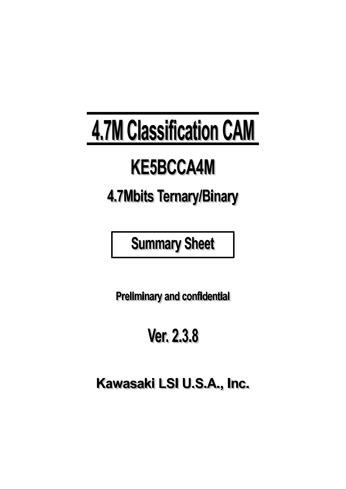
2. Block Diagram
Fig. 2-1 Functional Block Diagram
CEN
RWN
SAD
CLK
PHASE
RSTN
OEDATN
DAT[63:0]
EDAT[7:0]
DATWDT
CNTL[13:0]
PHOUN[1:0]
PHODN[1:0]
PMIN
PMON
FLIN[6:0]
FLON[1:0]
BHIDN
BHODN
BHIUN
BHOUN
BFLIN
SSHON
SMON
ODBYP
OEODN
OD[22:0]
PHIUN[6:0]
PHIDN[6:0]
INPMD
LMSTN
CLKMD
I/O
Port
Control
Control and
Status Registers
Pipeline
Execution
Control
Global Mask
Registers
CAM Control
Decoder
72bits x 65536
CAM
8 Banks
(72bitsx8Kx8)
structure
Mixable with
72bits x 8192
144bits x 4096
288bits x 2048
Empty Bit
Flag Control Output Port Control
Priority Encoder
Page 5

Kawasaki LSI
4.7M Classification CAM PRELIMINARY
Version 2.3.8 3 Confidential
The KE5BCCA4M has the following components:
• I/O Port Control
I/O port to input search key data and read/write data. I/O port data bus can be configured as a
72-bit or 40-bit wide bus.
• Pipeline Execution Control
Controls operation with pipeline through the CNTL [13:0].
• Control/Status Register
Defines CAM functions.
• Mask Registers
18 Global Mask Registers in total: 16 72-bit wide user-definable registers and 2 fixed registers
(ALL 0 and ALL 1) for search and write operations.
• Search Logic/Control Logic
Controls CAM functions.
• CAM
72-bit x 64k CAM data table divided into 8 banks. Each bank can be individually defined as a
72-bit x 8k, 144-bit x 4k, or 288-bit x 2k (Binary/Ternary), and it is possible to search a specific
bank or several banks at the same time. By using these features, various kinds of data for
Layer-2, 3 and 4 can be stored in one device and managed in different ways.
• Output Port Control
Controls output port, which outputs search results. The DAT data bypass function is provided
for the external SRAM access through this CAM device.
• Flag Logic
Controls the flag status (e.g. Full and Hit). Interfaces with other devices in a cascaded system.
When the CAM table is divided into multiple blocks, the status of the searched block is output.
Page 6
Kawasaki LSI
4.7M Classification CAM PRELIMINARY
Version 2.3.8 4 Confidential
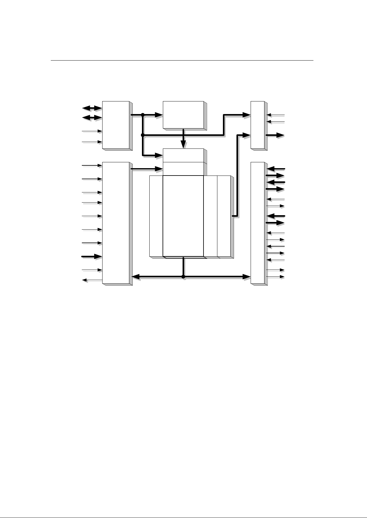
3. Pin Descriptions
3.1. Pin Assignment
Refer to the datasheet.
3.2. Pin Descriptions
Pin Name Description Attribute Function
RSTN Hardware Reset Input RSTN low resets the device.
CLK Clock Input CLK is the clock input. The rising edge of CLK is the timing
reference.
INPMD Input Mode Input INPMD determines the data input mode. Fix low in high-speed
input mode; fix high in normal speed input mode.
PHASE Phase Input PHASE determines the action timing of the device in high-speed
input mode. PHASE must be pulled down in normal input mode.
CLKMD Clock Mode Input CLKMD determines the CLK input method. Fix low in normal
speed input mode. In high-speed input mode, when supply
single rate clock, fix low and the double rate clock is generated
internally; when supply double rate clock, fix high.
DAT[63:0] I/O Port
Data Bus
Input/
Output
Tristate
DAT[63:0] is a 64-bit bi-directional data bus for read/write of
CAM memory and registers. RWN controls the bus direction.
EDAT[7:0] EXTRA Bit Data
Bus
Input/
Output
Tristate
EDAT[7:0] is a 8-bit bi-directional data bus for read/write of
EXTRA bits of CAM memory and registers. RWN controls the
bus direction.
DATWDT I/O Port Data Bus
Width
Input DATWDT defines DAT[63:0] width. Fix low to employ all
DAT[63:0]; fix high not to employ DAT[63:32] and to employ
DAT[31:0] with SAD as a substitute for DAT[63:0].
CNTL[13:0] Control Bus Input CNTL[13:0] is the 14-bit control bus to control the device. The
search operations, the command assertions, and the register
accesses are invoked corresponding to CNTL[13:0].
SAD Sub Address Input SAD assigns DAT[31:0] to internal 64-bit data bus when
DAT[63:32] is unused (DATWDT=high). When SAD is low,
DAT[31:0] is assigned to lower 32-bit; when high, it is assigned
to upper 32-bit.
CEN Device Enable Input CEN low invokes operations such as read/write, search and
command.
RWN Read/Write Input RWN determines the direction of the I/O Port data bus
DAT[63:0] and that of the EXTRA bit data bus EDAT[7:0]. RWN
low selects a write cycle and RWN high selects a read cycle.
OEDATN I/O Port Data Bus
Output Enable
Input OEDATN is output enable signal for DAT[63:0] and EDAT[7:0].
Page 7

Kawasaki LSI
4.7M Classification CAM PRELIMINARY
Version 2.3.8 5 Confidential
Pin Name Description Attribute Function
OD[22:0] Output Port
Output
Output
Tristate
OD[22:0] is a 23-bit output port. Valid flag, Device ID, Highest
Hit Address (HHA), or Highest Empty Address (HEA) are
output.
OEODN Output Port
Output Enable
Input OEODN is output enable signal for OD[22:0].
ODBYP Output Port
Bypass Control
Input When ODBYP is high, the input data to I/O Port (DAT bus) is
output to Output Port (OD bus).
LMSTN Longest Match
Status Output
Output LMSTN stays low during the execution of Longest Match
Search.
SSHON Synchronous Hit
Output
Output SSHON outputs the search results in the device synchronous
with CLK. SSHON low indicates a hit (match) and SSHON high
no entry hit (miss) in the search operation. The SSHON of the
bottom device (Last Device) indicates the hit of a cascaded
system.
SMON Synchronous
Multi-Hit
Output
Output SMON outputs the search results in the device synchronous
with CLK. SMON low indicates a multi-hit (multiple matches)
and SMON high no multi-hit in the search operation.
SMON shows the multiple hit status of the device and does not
show the system's status even in the cascaded system.
PHIDN[6:0] Priority Hit
Down Input
Input PHIDN[6:0] connects devices for cascading operations. Refer to
Datasheet.
PHODN[1:0] Priority Hit
Down Output
Output PHODN[1:0] is used for cascade connection. PHODN[1:0] low
indicates a hit (match) and PHODN[1:0] high no hit entry (miss)
in the search operation.
PHIUN[6:0] Priority Hit Up
Input
Input PHIUN[6:0] connects devices for cascading operations. Refer to
Datasheet.
PHOUN[1:0] Priority Hit Up
Output
Output PHOUN[1:0] is used for cascade connection. PHOUN[1:0] low
indicates a hit (match) and PHOUN[1:0] high no hit entry (miss)
in the search operation.
PMIN Priority Multi-Hit
Input
Input PMIN connects devices for cascading operations. Refer to
Datasheet.
PMON Priority Multi-Hit
Output
Output PMON is a output pin that outputs the search results. PMON
low indicates a multi-hit (multiple matches) and PMON high no
multi-hit in the search operation.
The PMON pin of the lowest priority device (Last Device)
indicates the hit signal of the cascaded system.
Page 8

Kawasaki LSI
4.7M Classification CAM PRELIMINARY
Version 2.3.8 6 Confidential
Pin Name Description Attribute Function
FLIN[6:0] Full Flag input Input FLIN[6:0] is used in the cascaded system. Refer to Datasheet.
FLON[1:0] Full Flag Output Output FLON[1:0] outputs the full status of the CAM memory.
FLON[1:0] low indicates all entries in the CAM memory are filled
with valid entries (full status) precluding a new registration.
The FLON pin of the lowest priority device (Last Device)
indicates the hit signal of the cascade configuration.
BHIDN Block Priority
Hit Down input
Input BHIDN is used in a cascaded system composed by more than 8
devices.
BHODN Block Priority Hit
Down output
Output BHODN is used in a cascaded system composed by more than
8 devices.
BHIUN Block Priority Hit
Up input
Input BHIUN is used in a cascaded system composed by more than 8
devices.
BHOUN Block Priority Hit
Up output
Output BHOUN is used in a cascaded system composed by more than
8 devices.
BFLIN Block Empty
Priority input
Input BFLIN is used in a cascaded system composed by more than 8
devices.
PLLEN PLL Enable Input PLLEN enables internal PLL. Refer to Datasheet for detail.
CPOUT Charge Pump Out Output CPOUT interfaces an off-chip loop filter for internal PLL. Refer
to Datasheet for detail.
VCOIN VCO Input Input VCOIN interfaces an off-chip loop filter for internal PLL. Refer to
Datasheet for detail.
VCOSEL VCO Select Input Input VCOSEL selects internal VCO (Voltage Controlled Oscillator).
Refer to Datasheet for detail.
MACROOPSEL Macro Option
Select
Input MACROOPSEL defines parameters of internal circuitry. Refer
to Datasheet for detail.
TESTMODE[1:0] Test Mode Select Input TESTMODE[1:0] select test mode of internal circuitry. Refer to
Datasheet for detail.
VDDQ Power (I/O) Power Power supply: 1.8V ± 0.15V, 2.5V ± 5% or 3.3V ± 5%
VDD Power (core) Power Power supply: 1.8V ± 0.15V
GND Ground Ground Ground
Page 9

Kawasaki LSI
4.7M Classification CAM PRELIMINARY
Version 2.3.8 7 Confidential
4. Functional Descriptions
4.1. Overview
KE5BCCA4M has a dual-port architecture: I/O port and Output port. The I/O port is for search key
data input and command input. The output port is for the search result output.
Commands are asserted through the CNTL [13:0] bus. Read/write of stored data and search key
data are provided through DAT[63:0] and EDAT[7:0]. This 72-bit bus (DAT[63:0] and EDAT[7:0]) can
be defined as 72-bit or 40-bit.
The CAM table consists of 8 banks, each of which can be configured as Ternary and Binary and in
table widths of 72-bit, 144-bit or 288-bit. The search operation can be performed simultaneously on
multiple banks of the same configuration.
The CAM also provides the function called Weighted Search without data sorting. That is,
regardless of the order of the data stored, the most weighted entry is output when a search
operation results in multiple hit.
4.2. Segment Structure
4.3. Output Format
Local Data
Empty
Bit
Local Mask Data
Hit
Flag
Data 64bitsExtra 8bits
71 64 63 0
Classification
CAM
HHA/HEA[15:0]
0
Device ID[4:0]
HHA/HEA Flag (0:HHA, 1:HEA)
OEODN
OD[22:0]
SSHON
SMON
15
DEVID[4:0]
16202122
Valid Flag (0:Valid, 1:Invalid)
Page 10

Kawasaki LSI
4.7M Classification CAM PRELIMINARY
Version 2.3.8 8 Confidential
4.4. CAM Table Example
+
MASK 0
MASK 1
MASK 2
MASK 15
ALL 0 MASK
ALL 1 MASK
INPUT Data
BANK0 BANK1 BANK2 BANK3
BANK4 BANK5 BANK6 BANK7
Layer 2
Binary CAM
72bits
x 8k entries
Layer 3
Ternary CAM
72bits
x 8k entries
Layer 4
Ternary CAM
144bits
x 4k entries
Layer 4
Ternary CAM
288bits
x 2k entries
Layer 2
BinaryCAM
72bits
x 8k entries
Layer 3
Ternary CAM
72bits
x 8k entries
Layer 4
Ternary CAM
144bits
x 4k entries
Layer 4
Ternary CAM
144bits
x 4k entries
Configurable CAM Table(Binary/Ternary or Bit width for Each BANK)
Example:
Configurable CAM Table
Selection Control
- Layer 2(BANK0,1)
- Layer 3(BANK2,3)
- Layer 4(BANK4,5,6)
- Layer 4(BANK7)
Mask Selection
Key Data
OUTPUT Data
HHA
HIT
MHIT
Page 11

Kawasaki LSI
4.7M Classification CAM PRELIMINARY
Version 2.3.8 9 Confidential
4.5. CNTL Bus (CNTL[13:0])
The CNTL bus (CNTL[13:0]) defines the operation. The function of the CNTL bus is classified into
four categories as follows:
• The control of a search operation
• The control of a weighted search operation
• The control of a command
• The control of an access to a register
As shown below, CNTL[13:12] defines the operation, and CNTL[11:5] defines the parameters, and
CNTL[4:0] defines the Mask Register number. As for the parameters and the Mask Register number,
refer to the datasheet.
1 0 Address Field
Global
Mask
Register control
13 12 11 5 4 0
0 0 Operation Field
Global
Mask
Command control
13 12 11 5 4 0
1 1 Search Operation Field
Global
Mask
Weighted Search
control
13 12 11 5 4 0
0 1 Search Operation Field
Global
Mask
Normal Search control
13 12 11 5 4 0
0
10
Page 12

Kawasaki LSI
4.7M Classification CAM PRELIMINARY
Version 2.3.8 10 Confidential
4.6. Timing Chart
(1) Timing Chart of Search --- Normal Input Mode
*1: This shows the case that both EXL[1:0] and CSM of the CNTL Register are set to ‘00’ and
‘0’ respectively. Refer to Datasheet for other cases.
*2: This shows the case that EXL[1:0] of the CNTL Register is set to ‘00’. Refer to Datasheet
for other cases.
*3: This shows the case that both EXL[1:0] and ODL of the CNTL Register are set to ‘00’ and
‘0’ respectively. Refer to Datasheet for other cases.
CLK
PHASE
CEN
CNTL[13:0]
SAD
RWN
Latency 4 Cycle (*2)
Latency 3 Cycle (*1)
#0
#n
#n
Tpd
Tpd
Hit #0 & #1
#0
DAT[63:0]
EDAT[7:0]
SRCH
SEG
#n
SEG
#n
72bits Search
SSHON
SMON
OD[22:0]
Multiple
#0 & #1
Latency 4 Cycle (*3)
#n
Tpd
#0
INDEX
#0 & #1
AND
SRCH
SRCH
SEG
#1
SEG
#1
SEG
#0
SEG
#0
144bits Search
AND
SRCH
AND
SRCH
SRCH
SEG
#1
SEG
#1
SEG
#2
SEG
#2n
SEG
#0
SEG
#0
216bits Search
LOW
Page 13

Kawasaki LSI
4.7M Classification CAM PRELIMINARY
Version 2.3.8 11 Confidential
(2) Timing Chart of Search --- High-speed Input Mode for 72bits/144bits
*1: This shows the case that both EXL[1:0] and CSM of the CNTL Register are set to ‘00’ and
‘0’ respectively. Refer to Datasheet for other cases.
*2: This shows the case that EXL[1:0] of the CNTL Register is set to ‘00’. Refer to Datasheet
for other cases.
*3: This shows the case that both EXL[1:0] and ODL of the CNTL Register are set to ‘00’ and
‘0’ respectively. Refer to Datasheet for other cases.
CLK or
CLKX2
PHASE
CEN
CNTL[13:0]
SAD
RWN
Latency 4 Cycle (*2)
Latency 3 Cycle
(*1)
#0
#n
#n
Tpd
Tpd
Hit #2n & #2n+1
#0
DAT[63:0]
EDAT[7:0]
SRCH
SEG
#n
SEG
#n
SSHON
SMON
OD[22:0]
Multiple
#2n & #2n+1
Latency 4 Cycle (*3)
#n
Tpd
#0
INDEX
#2n & #2n+1
AND
SRCH
SRCH
AND
SRCH
SRCH
SEG
#1
SEG
#1
SEG
#2n
SEG
#2n
SEG
#2n+1
SEG
#2n+1
SEG
#0
SEG
#0
144bits Search 144bits Search
AND
SRCH
AND
SRCH
AND
SRCH
SRCH
SEG
#1
SEG
#1
SEG
#2
SEG
#2n
SEG
#3
SEG
#2n+1
SEG
#0
SEG
#0
288bits Search72bits Search
Page 14

Kawasaki LSI
4.7M Classification CAM PRELIMINARY
Version 2.3.8 12 Confidential
(3) Timing Chart of Ternary CAM R/W --- High-speed Input Mode
Single rate clock mode (CLKMD=Low)
Double rate clock mode (CLKMD=High)
*1: This shows EXL[1:0] of the CNTL Register is set to ‘00’. Refer to datasheet for other
cases.
Latency 3 Cycle
(*1)
Latency 3 Cycle
(*1)
CLK
PHASE
CEN
CNTL[13:0]
SAD
DAT[63:0]
EDAT[7:0]
Local
Data1
RWN
Local
Data1
MEM
INC
MEM
Local
Mask
Data3
Local
Mask
Data3
Local
Data3
Local
Data3
MEM
INC
Local
Data0
Local
Data0
OEDATN
Tpd
Tpd
Local
Mask
Data0
Local
Mask
Data0
MEM
Local
Mask
Data1
Local
Mask
Data1
MEM
MEM
INC
MEM
INC
MEM
1 UNIT (144bits Write)
MEM
INC
MEM
Local
Mask
Data4
Local
Mask
Data4
Local
Data4
Local
Data4
Local Data Local Mask Data
Local
Data2
Local
Data2
Local
Mask
Data2
Local
Mask
Data2
1 UNIT (72bits Write)
Local Data Local Mask Data
1 UNIT (Read)
Local Data Local Mask Data
1 UNIT (Read)
Local Data Local Mask Data
Latency 3 Cycle
(*1)
Latency 3 Cycle
(*1)
(Internal
CLKX2)
PHASE
CEN
CNTL[13:0]
SAD
DAT[63:0]
EDAT[7:0]
Local
Data1
RWN
Local
Data1
MEM
INC
MEM
Local
Mask
Data3
Local
Mask
Data3
Local
Data3
Local
Data3
MEM
INC
Local
Data0
Local
Data0
OEDATN
Tpd
Tpd
Local
Mask
Data0
Local
Mask
Data0
MEM
Local
Mask
Data1
Local
Mask
Data1
MEM
MEM
INC
MEM
INC
MEM
1 UNIT (144bits Write)
MEM
INC
MEM
Local
Mask
Data4
Local
Mask
Data4
Local
Data4
Local
Data4
Local Data Local Mask Data
Local
Data2
Local
Data2
Local
Mask
Data2
Local
Mask
Data2
1 UNIT (72bits Write)
Local Data Local Mask Data
1 UNIT (Read)
Local Data Local Mask Data
1 UNIT (Read)
Local Data Local Mask Data
CLK
Page 15

Kawasaki LSI
4.7M Classification CAM PRELIMINARY
Version 2.3.8 13 Confidential
5. Command Descriptions
*1: In the normal speed mode, 1-Cycle means 1-CLK but in the high-speed mode, 1-Cycle
means 2-CLK as with the access to the registers.
Command
Group
Command name
CNTL[13:0]
Cycle
No. *1
Function
Description
Reset
SRST
(00_0000_0000_0000)
2
Software
reset
Execute Device reset as with the RSTN low. The
flag pins are set as follows:
PHOUN[1:0]=High, PHODN[1:0]=High,
PMON=High, FLON[1:0]=High, SSHON=High,
SMON=High, LMSTN=High
Configuration
STR_DEVID
(00_0001_0000_0000)
1
DEVID
mode start
Enter the DEVID mode for the Device ID
registration in a cascaded system.
END_DEVID
(00_0010_0000_0000)
1
DEVID
mode end
Exit the DEVID mode.
NXT_PR
(00_0011_0000_0000)
1
Shift
DEVID
priority
Shift the DEVID priority to the next device in the
DEVID mode.
Search
SRCH
(01_QRSS_TTTU_UUUU)
1 Search
Execute normal search.
Refer to Datasheet for Q, R, S, T, and U field.
WT_SRCH
(11_Q0SS_TTTU_UUUU)
1 Search
Execute Weighted Search.
Refer to Datasheet for Q, S, T, and U field.
CAM table
PRG_AL
(00_0100_0000_0000)
1 Purge
All entries become empty (inactive).
PRG_HIT
(00_0101_0000_0000)
1 Purge
All hit Entries become empty (inactive). This
command is effective only for the last searched
Logical Bank.
PRG_HHA
(00_0110_0000_0000)
1 Purge
The CAM Entry designated by the HHA Register
becomes empty (inactive). In a cascaded system,
the hit priority must be fixed prior to the command
execution. This command is effective only for the
last searched Logical Bank.
PRG_DA
(00_0111_0000_0000)
1 Purge
The CAM Entry designated directly through
DAT[31:0] becomes empty (inactive). Refer to
Datasheet.
GEN_FL
(00_1110_TTT0_0000)
1
Update the
HEA
address
Update empty status of the CAM table, which
means the HEA Register and FLON[1:0] are
updated. T field specifies the Logical Bank. Refer
to Datasheet.
Page 16

Kawasaki LSI
4.7M Classification CAM PRELIMINARY
Version 2.3.8 14 Confidential
*1: In the normal speed mode, 1-Cycle means 1-CLK; but in the high-speed mode, 1-Cycle
means 2-CLK as with the access to the registers.
*2: When the Store command is executed for a Binary CAM Bank, 1-Cycle is required; but
when it executed for a Ternary CAM Bank, 2-Cycle is required.
Command
Group
Command name
CNTL[13:0]
Cycle
No. *1
Function
Description
Store
STR_AR
(00_1000_SSTU_UUUU)
1 or 2
*2
Store
Store data of the CMP Register to a CAM Entry
designated by the AR Register. S field specifies
the number of both CMP Register and Segment.
Refer to Datasheet for S, T, and U field.
STR_HHA
(00_1001_SS0U_UUUU)
1 or 2
*2
Store
Store data of the CMP Register to a CAM Entry
designated by the HHA Register. S field specifies
the number of both CMP Register and Segment.
Refer to Datasheet for S and U field.
STR_HEA
(00_1010_SS0U_UUUU)
1 or 2
*2
Store
Store data of the CMP Register to a CAM Entry
designated by the HEA Register. S field specifies
the number of both CMP Register and Segment.
Refer to Datasheet for S and U field.
STR_AUT
(00_1011_SS0U_UUUU)
1 or 2
*2
Store
When the last search result is hit, do the
STR_HHA operation. When miss, do the
STR_HEA operation with no mask. S field
specifies the number of both CMP Register and
Segment. Refer to Datasheet for S and U field.
Other
NOP
(00_1111_0000_0000)
1
No
operation
Execute no operation.
Page 17

Kawasaki LSI
4.7M Classification CAM PRELIMINARY
Version 2.3.8 15 Confidential
6. Register
The followings show the registers.
CNTL Register, LOGICAL BANK CNTL Register
DEVID Register, STAT Register
MASK 0,1,2,3,4,5,6,7,8,9,10,11,12,13,14,15 Register
CMP 0,1,2,3 Register, CMPLM 0,1,2,3 Register
AR Register, MEMAR Register, MEMARIN Register
SEG Register,
HHA Register, MEMHHA Register, MEMHHA_SI Register
HEA Register, MEMHEA Register, MEMHEA_SI Register
7. Product Information
7.1. Ordering Information
7.2. Package Outline
0.15 S
24.13 0.20
0.60 0.10
2.36 0.20
0.750 0.15
INDEX
UNIT: mm
27.00 0.20
24.00 0.10
2019181716151413121110
987654321
Y W V U T R P N M L K J H G F E D C B A
1.27 0.2
View from bottom
View from top
Part No. Package Description
core
I/O
KE5BCCA4MCBP-E 324-pin BGA 1.8V 1.8V
Revision E of the KE5BCCA4M
Classification CAM with 1.8V I/O
KE5BCCA4NCBP-A 324-pin BGA 1.8V 2.5V/3.3V
Revision A of the KE5BCCA4M
Classification CAM with 2.5V/3.3V I/O
Power Supply
Page 18

Kawasaki LSI
4.7M Classification CAM PRELIMINARY
Version 2.3.8 16 Confidential
8. Electrical Characteristics
8.1. Absolute Maximum Rating
*1: 1.8V I/Os are not 2.5V, 3.3V or 5V tolerant; 2.5V/3.3V I/Os are not 5V tolerant.
8.2. Operating Range
8.3. DC Characteristics
*1: Several parameters are required to estimate power consumption. Refer to the datasheet.
*2: For DAT[63:0] and EDAT[7:0], IOL=4mA/IOH=-4mA; for other pins, IOL=8mA/IOH=-8mA.
ITEM
SYMBOL
MIN.
TYP.
MAX.
UNIT
Supply Voltage (1.8V I/O)
V
DDQ
1.65
1.8
1.95VSupply Voltage (2.5V I/O)
V
DDQ
2.375
2.5
2.625
V
Supply Voltage (3.3V I/O)
V
DDQ
3.135
3.3
3.465
V
Supply Voltage (core)
VDD1.65
1.8
1.95
V
Ambient Operation Temperature
TA0+25
+70
ºC
ITEM
SYMBOL
MIN.
TYP.
MAX.
UNIT
CONDITION
Input Low Voltage (1.8V I/O)
VIL
-0.3
0.35V
DDQ
V
Input High Voltage (1.8V I/O)
VIH
0.65V
DDQ
V
DDQ
+0.3
V
Output Low Voltage (1.8V I/O)
VOL
+0.45
V
IOL=8mA or 4mA
*2
Output High Voltage (1.8V I/O)
VOH
V
DDQ
-0.45VIOH=-8mA or -4mA
*2
Input Low Voltage (2.5V I/O)
VIL
T.B.D.
T.B.D.
V
Input High Voltage (2.5V I/O)
VIH
T.B.D.
T.B.D.
V
Output Low Voltage (2.5V I/O)
VOL
T.B.D.
V
Output High Voltage (2.5V I/O)
VOH
T.B.D.
V
Input Low Voltage (3.3V I/O)
VIL
0.8
V
Input High Voltage (3.3V I/O)
VIH
2.0
V
Output Low Voltage (3.3V I/O)
VOL
0.4
V
Output High Voltage (3.3V I/O)
VOH
2.4VInput Leakage Current
IIL
-10µAVIN=GND
IIH
+10µAVIN=VDD
Output Leakage Current
IOZ
-10
+10µAOutput is high impedance
Standby Current
IDDS
T.B.D.
µA
Dynamic Operation Current
IDDOP
*1
mA
ITEM
SYMBOL
STANDARD CONDITION
UNIT
NOTE
Supply Voltage (1.8V I/O)
V
DDQ
-0.3 ~ +2.2
V
Supply Voltage (2.5V I/O)
V
DDQ
T.B.D.
V
Supply Voltage (3.3V I/O)
V
DDQ
-0.3 ~ +4.0
V
Supply Voltage (core)
VDD-0.3 ~ +2.2
V
Input Voltage
VI
-0.3 ~ V
DDQ
+ 0.3
V*1Output Voltage
VO
-0.3 ~ V
DDQ
+ 0.3
V*1I/O Voltage
VIO
-0.3 ~ V
DDQ
+ 0.3
V
*1
Storage Temperature
TSTG
-55 ~ +125
ºC
Page 19

Kawasaki LSI U.S.A., Inc.
Silicon Valley Office Eastern Area Office
2570 North First Street, Suite 301 201 Edgewater Drive, Suite 251
San Jose, CA 95131 Wakefield, MA 01880
Tel: (408)570-0555 Tel: (781)224-4201
Fax: (408)570-0567 Fax: (781)224-2503
URL: www.klsi.com
Kawasaki LSI U.S.A., Inc. (herein after KLSI) reserves the right to make changes
herein at any time without notice. KLSI does not assume any responsibility or liability
arising out o
f application or use of any product described herein, neither does it convey
any license under its patent rights nor the rights of others.
KLSI products are not designed, intended, or authorized for use as components in
systems intended for surgical implan
t into the body, or other applications intended to
support or sustain life, or for any other applications in which the failure of the KLSI
product could create a situation where personal injury or death may occur.
 Loading...