

Page 1

Ver. 1.2.1
ADDRESS PROCESSOR
64k-bit • 3-port type
KE5B256B1
Page 2

Address Processor KE5B256B1
Table of Contents
1. Features
1.1 Introduction
1.2 Functional Overview
1.3 Specifications
1.4 Register Names
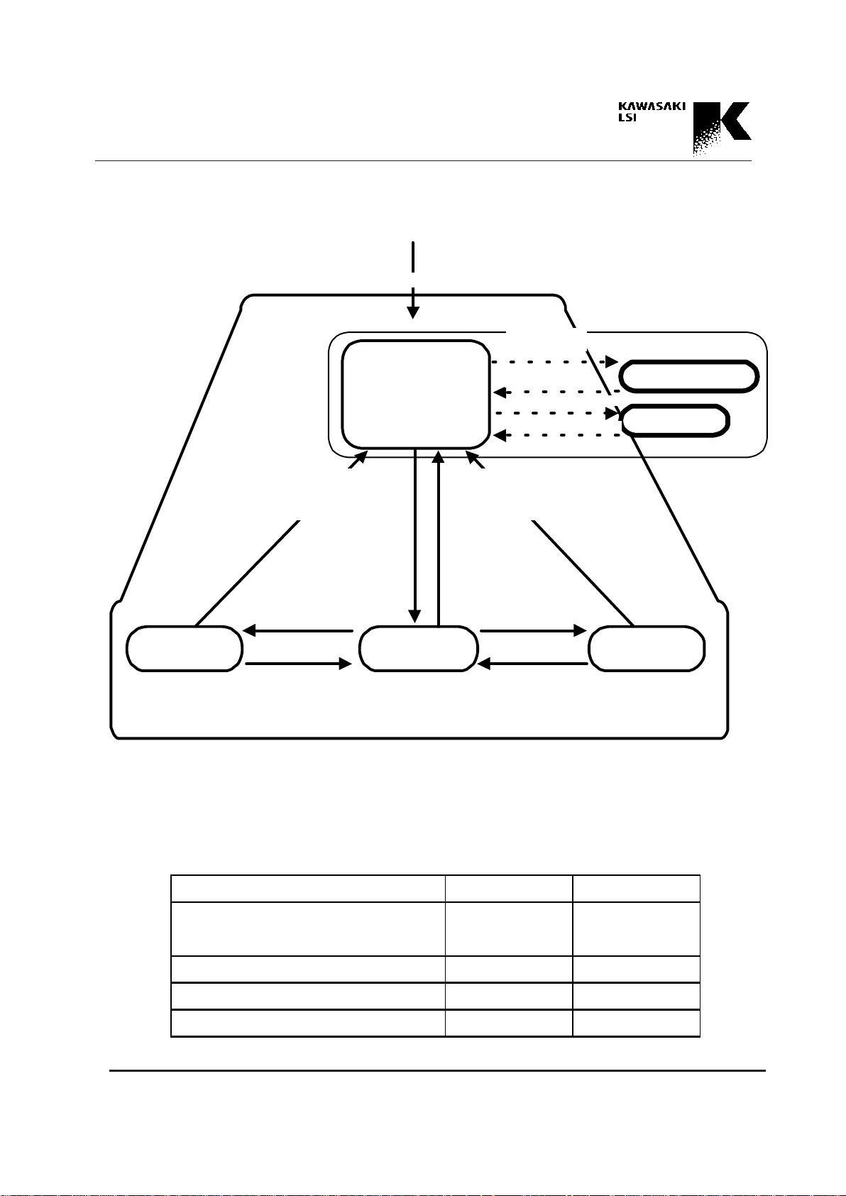
2. Block Diagram
3. Pin Assignment and Pin Descriptions
3.1 Pin Assignment
3.2 Pin Descriptions
4. Port and Operation Mode Overview
4.1 Port Overview
4.2 Arbitration
4.3 Operation Modes Overview
4.4 External Arbitration
5. CAM Table
5.1 Entry and Segment
5.2 Table Configuration
5.3 Read/Write Segment Data
5.4 Search and CAM Table
6. Input Port
6.1 Input Port Configuration
6.2 IP Sequence Configuration
6.3 Selection of Channel and Start Sequence Number
6.4 IP Sequence Operation
6.5 HHA Automatic Output
7. Output Port
7.1 OP Sequence Configuration
7.2 Selection of Channel and Start Sequence Number
7.3 OP Sequence Operation
8. CPU Port
8.1 Access to Registers
8.2 Basic Operation through CPU Port
8.3 Search Operation through CPU Port
8.4 Search Result Output from CPU Port
8.5 HHA/HEA Register Operation
8.6 Automatic Increment Function
8.7 Table Maintenance
9. Cascading
9.1 Device ID Registration
9.2 Priority
9.3 Cascade Connection
9.4 Input Port in a Cascade System
9.5 Output Port in a Cascade System
9.6 CPU Port in a Cascade System
9.7 AC Characteristics in a Cascade System
9.8 Single Device Operation
10. Initialization
11. Examples
12. Command Descriptions
12.1 Command Functions
12.2 Conditions for Executing Commands
13. Register Descriptions
13.1 Overview
13.2 Register Addresses
13.3 Register Bit Maps
13.4 Conditions for Accessing Registers
14. Electrical Characteristics
14.1 Absolute Maximum Ratings
14.2 Operating Range
14.3 DC Characteristics
14.4 AC Characteristics
15. Package Outline
Page 3

1-1
Address Processor KE5B256B1
1. Features
1.1 Introduction
KE5B256B1 is a 256k-bit CAM (Content Addressable
Memory) device with a new architecture. The main function of the LSI is fast searching of data on the search data
table stored in CAM. User can define the row/column table
size flexibility. The width of one entry in the search data
table can be selected from 32 bits to 256 bits, in increments
of 32 bits (1 segment). User can define the area to be
searched in an entry freely in terms of the position and bit
width. The search operation is executed for each segment,
and the cycle time is 80ns with the fast operation characteristic of CAMs. KE5B256B1 provides 3 ports, an Input
Port, Output Port and CPU Port. These ports are designed
to have the most appropriate functionality.
The Input Port, which is only used for inputting the key
data, provides the programmable input data formatter and
programmable sequencer. These capabilities enable the
formatting of the incoming key data and flexible search
operation with any table column as a pre-determined sequence by writing into the Input Port.
Therefore, user can execute complex search operations
quickly. The search results can be output by flag pin and
by register reading from the Output Port or the CPU Port.
The Output Port is only used for outputting the search results. Like the Input Port, it has a programmable sequencer. The Output Port can output search results automatically according to a pre-determined sequence by reading from the Output Port.
The CPU Port is used for the definition of the search table,
the table configuration/maintenance and the configuration
of the Input Port and the Output Port . The CPU Port has
registers and commands by which user can realize functions easily. The registers can be accessed with direct addressing, and there are various effect commands for table
maintenance. The input/output data bus is 16 bits in width.
An endian function is supported to make it easy to access
the search table data of 32 bits. The upper 16 bits or the
lower 16 bits of the segment can be read/written with the
same address using the endian function.
Multiple devices can be easily cascade-connected in order
to increase the number of entries in the CAM table without
external logic. The extended CAM realized by cascade
connection can be treated as if it were one continuous table
in one device, because priority control is done internally
between devices.
However, the number of segments forming one entry in the
search data table must be the same in all devices (even if
the devices are not cascade connected).
This device must arbitrate between ports to protect against
data destruction caused by simultaneous access from plural ports. User can select two methods of arbitration. One
is an internal arbitration mode which restricts the device to
internal operation by port-dependent modes (CPU mode,
IP mode, OP mode, IOP mode). In this case, the device
determines whether the device receives operations from
every port or not. The other is external arbitration. In this
case, simultaneous access from every port is not permitted.
However, user can decrease the execution cycles, because
instead of external arbitration, mode restriction is not applied. User can select either method according to the required applications.
Page 4

1-2
Address Processor KE5B256B1
1.2 Functional Overview
The KE5B256B1 (Address Processor: AP) provides the
best solution to the fast and complex "Address Filtering"
requirements of today's internetworking equipment with
the following outstanding functions.
(1) Flexible search data table definition answering to various protocols.
• The entry size is configurable from 32 bits to 256
bits.
• The search operation of any width key data can be
performed with data at any position in the table.
• All the CAM area can be accessed as RAM.
(2) 3-port architecture
• Optimized functionality for each port provides
fast data processing.
(3) Programmable input data formatting and search sequence
• The input data width can be selected as 32, 16, or
8 bits.
• Definition of data input and search start position.
• Masking by bit is possible.
• Search window set by byte unit.
• Maximum 8 step search sequence definition
to any column of the table.
(4) Programmable output sequence
• Output sequence definition of any search
result.
• Output sequence definition of any column of
the hit entry.
(5) Multi-channel sequence
• A maximum of 16 kinds of IP sequences and OP
sequences can be defined by indicating the channel/
number of the start sequence.
(6) Cascading
• No additional logic is required.
• A cascaded table acts as one integral search data.
(7) Commands
• Useful commands for the search table maintenance
1.3 Specifications
·
CA M core Capacit
y
256 kbits
Access to table entry Random access to all data
(RAM, CAM substitution)
Configuration Configurable to control the entry width from 32 b its to 256 bits
(Entry size) in units of 32 bits
• 32 bits x 8,192 entries
• 64 bits x 4,096 entries
• 96 bits x 2,728 entries
• 128 bit s x 2,048 en trie s
• 160 bit s x 1,636 en trie s
• 192 bit s x 1,364 en trie s
• 224 bit s x 1,168 en trie s
• 256 bit s x 1,024 en trie s
Cascad in
g
Up to 32 devices (adds table depth
)
Search Operatio n • Via C PU Port
• Via Inp ut Port (automatic)
• Masking by bit
• Search o peratio n by table segmen t (32 bits)
• AN D search f or mo re t ha n 32 bits of data
• H it accumulation using Access Bit
Result Ou tput • Via C PU Port
• Via Output Port (automatic)
• Hit result p in ( H O _)
• I ntermediate search result pins ( SH0_, SH1_)
•Hit
• Hit add ress
• Entry data of hit address
•
Key data use d in se arch o pe ration
Page 5
1-3
Address Processor KE5B256B1
Specifications (cont'd)
Ports I nput Port · Input data bl ock width is s electable (32, 16, or 8 bits
)
(Key
data input
)
· Multi-channel:
IP sequence of 2 channels (A/B) can be defined.
Numb er of start sequence can be selected.
Input Port sequence Maximum 8-step input sequen ce co nf iguration and data
(
IP Sequence
)
formatting functions.
· Cut Through:
Any block selectable among 64 b locks in d ata stream
· Data Accumulation :
M ost recent 64 bit s can be temporarily stored
(Accu mulat io n Buf fer & Sub-accu mulation Buff er
)
· Search Window Set:
Key data selectable w ith 32-bit width among 64 b its of
accumulated data starting from n (n=0-3, n byte shift) byte
· Mask operation by bit
· Any segm en t can be searched in any order.
Output Port · 32 bits
(
Search result output
)
· Multi-channel
OP sequence of 2 channels (A/B) can be defined.
Numb er of start sequence can be selected.
Output Port sequence Maximum 8-step output sequen ce co nf iguratio n
(
OP Sequence
)
· Search key data:
Key data a fter d ata fo rmatting used in the IP sequence
(CMP0 - CMP7 register
)
· Hit status:
Hit, m u lt i- hit, used cha n nel (HSTAT register
)
· Hit address:
Hit entry add ress w ith the highest priority (HHA register
)
· Contents of hit add ress (MEMHHA register
)
* Hit status can be output in combin a t io n with ot her search results
CPU Port · 16-bit data, 8-bit addres s
· C o mm a n d ex ecut ion
· Regist er Rea d/Write
Sequence · SQRST_ (Pin
)
reset · SSQRST command (from CPU Port
)
Search resu lt · HO_: Result s of ea ch search operat io n
output pins · SH0_, SH1_: Interm edia t e search results of specified step in the IP sequence
Cycle time 80ns
I/F LVTTL compatible
Supply voltage 3.3V ± 0.3V
Package144-
p
in PQFP
T ech no lo
gy
0.5µ m CMOS
Page 6

1-4
Address Processor KE5B256B1
1.4 Register Names
Register names are described by the following abbreviations.
Abbreviations of Registers
Abbreviation Register Name
COM Register Command Register
CNTL Register Control Register
DEVID Register Device ID Register
DEVSTAT Register Device Status Register
DEVSEL Register Device Select Register
AR Register Address Register
MEMAR Register Memory_AR Register
MEMHHA Register Memory_HHA Register
MEMHEA Register Memory_HEA Register
CPUHS Register CPU HHA/HEA Segment Register
MEMAR_AT Register Memory_AR Attribute Register
MEMHHA_AT Register Memory_HHA Attribute Register
MEMHEA_AT Register Memory_HEA Attribute Register
SHASGN Register Sequence Hit Flag Assignment Register
HHASGN Register HHA Automatic Output Assignment Register
CUT Register Cut Register
SS Register Search Start Register
CS Register Channel Sequence Register
MASK Register Mask Register
AOC Register Automatic Output Control Register
AOSC Register Automatic Output Sub Control Register
CPUINP Register CPU Input Data Register
CPUMASK Register CPU Mask Register
CPUSRS Register CPU Search Segment Register
CPUINP2 Register CPU Input Data 2 Register
CPUMASK2 Register CPU Mask 2 Register
CPUSRS2 Register CPU Search Segment 2 Register
HSTAT Register Hit Status Register
ESTAT Register Empty Status Register
HHA Register Highest Hit Address Register
HEA Register Highest Empty Address Register
SH Register Sequence Hit Result Register
CMP Register Comparand Register
Page 7
2-1
Address Processor KE5B256B1
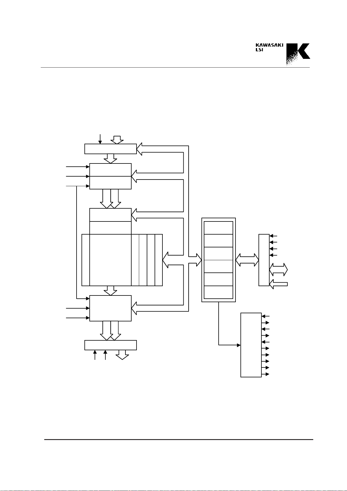
Fig. 2-1 Block Diagram
2. Block Diagram
OD<31:0>
Input Port (8, 16, 32 bits)
WR
ID<31:0>
Data Formatter
Input Port Sequencer
IPCH
ISNM<2:0>
SQRST_
32 bits
MASK 0 - 7
Comparison Logic
CAM Array
8,192 words 32bits
Decoder
Empty Bit
Hit Flag
Access Bit
Priority Encoder
32 bits
Output Port Sequencer
OPCH
OPNS
A ch
B ch
A ch
B ch
32 bits
Output Port
OE_
RD_
32 bits
Command
Control Status
Memory R/W
Configuration
CPU Search
Table Status
16 bits
CPU Port
16 bits
CE_
R/W_
RST_
SP/TP_
DAT<15:0>
ADD<7:0>
8 bits
Flag Logic
FLI_
FLO_
PI_
PO_
HI_
HO_
SH0_
SH1_
IPBUSY_/OPACT_
OPBUSY_/IPACT_
16 bits
Page 8
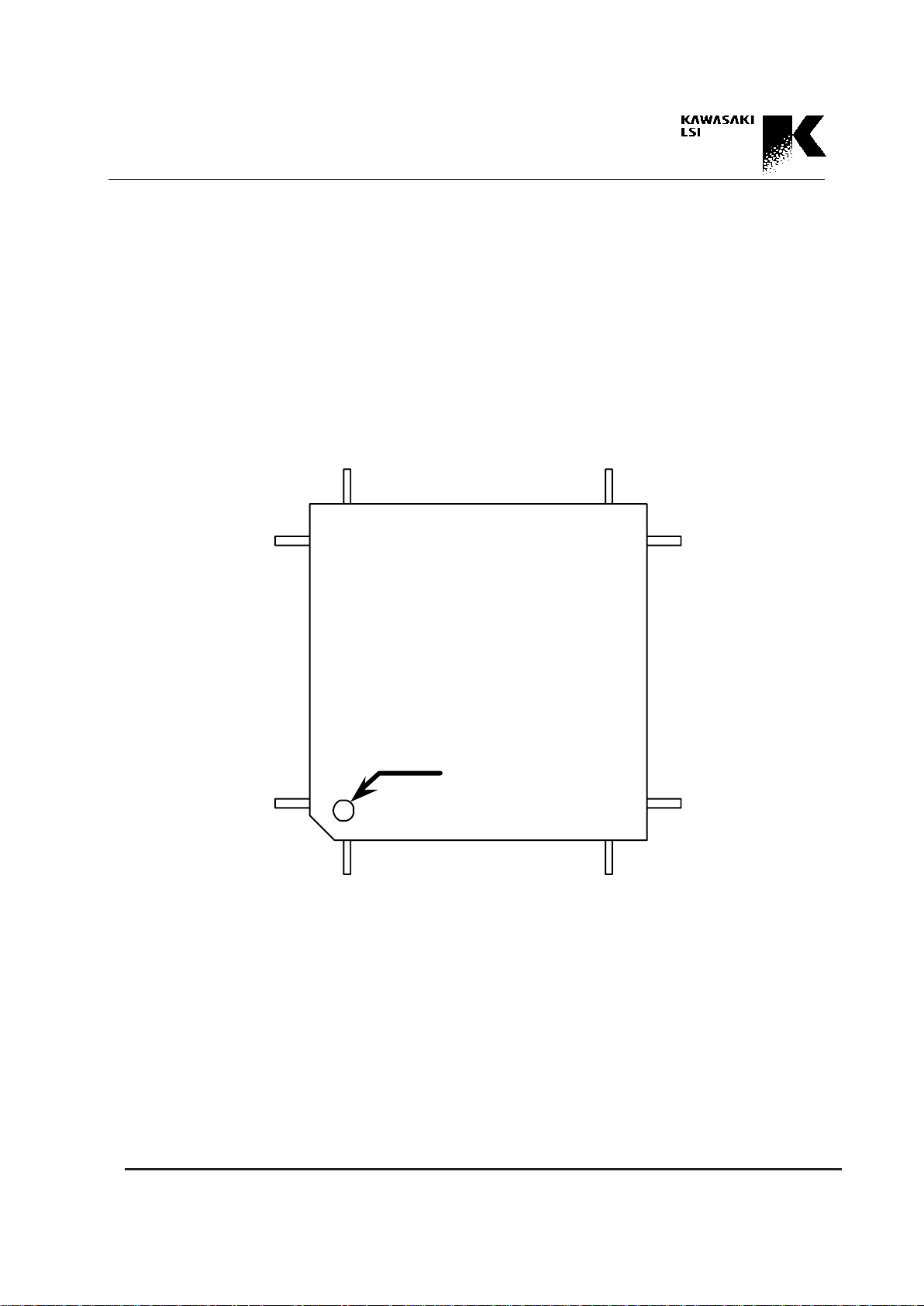
3-1
Address Processor KE5B256B1
Fig. 3.1.1 Pin Assignment
KE5B256B1CFP
(144-pin PQFP type)
3. Pin Assignment and Pin Descriptions
3.1 Pin Assignment
36
37
1
144
109
73
72
108
index
KE5B256B1CFP
QFP144
•
•
•
•
•
•
•
•
•
•
••••
••••
Page 9
3-2
Address Processor KE5B256B1
Table 3.1 Pin Assignment
Pin No. Signal Name I/O type Pin No. Signal Name I/O type
1 V DD - 41 ID<22> IN
2 OD<2> OUT 42 ID<23> IN
3 OD<1> OUT 43 ID<24> IN
4 OD<0> OUT 44 ID<25> IN
5 OE _ IN 45 ID<2 6> IN
6 PO _ OUT 46 ID<2 7> IN
7 PI_ IN 47 ID<28> IN
8 SH1_ OUT 48 ID<29> IN
9 SH0_ OUT 49 ID<30> IN
10 HO_ OUT 50 ID<31> IN
11 HI_ IN 51 IPBUSY _/OPACT_ OUT
12 FLO_ OU T 52 OPB US Y_/IPACT_ OUT
13 VDD - 53 WR IN
14 ID<0> IN 54 G ND 15 ID<1> IN 55 G ND 16 ID<2> IN 56 G ND 17 GND - 57 SQRST_ IN
18 GND - 58 RST_ IN
19 GND - 59 RD_ IN
20 ID<3> IN 60 ADD<0> IN
21 ID<4> IN 61 ADD<1> IN
22 ID<5> IN 62 ADD<2> IN
23 ID<6> IN 63 ADD<3> IN
24 ID<7> IN 64 ADD<4> IN
25 ID<8> IN 65 ADD<5> IN
26 ID<9> IN 66 ADD<6> IN
27 ID<10> IN 67 ADD<7> IN
28 ID<11> IN 68 G ND 29 ID<12> IN 69 R/W_ IN
30 ID<13> IN 70 CE_ IN
31 ID<14> IN 71 NC OPEN*1
32 ID<15> IN 72 V DD 33 ID<16> IN 73 V DD 34 ID<17> IN 74 DAT<0> IO
35 ID<18> IN 75 DAT<1> IO
36 VDD - 76 DAT<2> IO
37 VDD - 77 DAT<3> IO
38 ID<19> IN 78 DAT<4> IO
39 ID<20> IN 79 DAT<5> IO
40 ID<21> IN 80 G ND -
Page 10
3-3
Address Processor KE5B256B1
*1 NC pins should be open. (Do not connect.)
Table 3.1 Pin Assignment (cont'd)
Pin No. Signal Name I/O type Pin No. Signal Name I/O type
81 VDD - 121 OD<19> OUT
82 DAT<6> IO 122 OD<18> OUT
83 DAT<7> IO 123 OD<17> OUT
84 DAT<8> IO 124 OD<16> OUT
85 DAT<9> IO 125 GND 86 DAT<10> IO 126 GND 87 DAT<11> IO 127 GND 88 DAT<12> IO 128 OD<15> OUT
89 DAT<13> IO 129 OD<14> OUT
90 GND - 130 OD<13> OUT
91 GND - 131 OD<12> OUT
92 GND - 132 V DD 93 DAT<14> IO 133 OD<11> OUT
94 DAT<15> IO 134 OD<10> OUT
95 ISNM<0> IN 135 OD<9> OUT
96 ISNM<1> IN 136 OD<8> OUT
97 ISNM<2> IN 137 GND 98 OPNS IN 138 OD<7> OUT
99 IPCH IN 139 OD<6> OUT
100 OPCH IN 140 OD<5> OUT
101 G ND - 141 OD<4> OUT
102 OD<31> OUT 142 OD<3> OUT
103 OD<30> OUT 143 NC OPEN*1
104 OD<29> OUT 144 V DD 10 5 SP/TP_ IN
106 NC OPEN *1
107 FL I_ IN
108 V DD 109 V DD 110 OD<28> OUT
111 OD<27> OUT
112 OD<26> OUT
113 OD<25> OUT
114 OD<24> OUT
115 G ND 116 OD<23> OUT
117 OD<22> OUT
118 OD<21> OUT
119 OD<20> OUT
120 V DD -
Page 11

3-4
Address Processor KE5B256B1
Function
DAT<15:0>
ADD<7:0>
CE_
R/W_
RST_
ID<31:0>
3.2 Pin Descriptions
Pin name Attribute
CPU Port Data Bus
Input / Output
Tri-state LVTTL
CPU Port Address
Bus
Input
LVTTL
Device Enable
Input
LVTTL
Read/Write
Input
LVTTL
Hardware Reset
Input
LVTTL
Input Port
Data Bus
Input
LVTTL
DAT<15:0> is a 16-bit, bidirectional data bus used to convey data, commands, and status to and from the Address
Processor (AP). The direction is controlled by the state of
R/W_. DAT<15:0> is enabled by a low level of CE_.
ADD<7:0> is an 8-bit address bus used to select registers.
CE_ is used for access from the CPU Port. R/W_,
ADD, DAT inputs are latched on the falling edge of CE_.
R/W_ low selects a write cycle. R/W_ high selects a read
cycle. The state of R/W_ is registered on the falling edge of
CE_.
RST_ is a hardware reset signal. A low pulse of RST_ initializes the AP. The minimum low hold time is 40ns.
ID<31:0> is a 32-bit data bus used to convey search data to
the AP through the Input Port. The ID bus width can also
be configured to 8 bits (ID<7:0>) or 16 bits (ID<15:0>).
Page 12

3-5
Address Processor KE5B256B1
FunctionPin Name Attribute
Input Port
Write Pulse
Input
LVTTL
Port Number
Select
Input
LVTTL
Input/Output
Port Sequence
Pointer Reset
Input
LVTTL
Output Port
Data Bus
Output
LVTTL
Output Port
Read Pulse
Input
LVTTL
Output Port
Outpt Enable
Input
LVTTL
WR
SP/TP_
SQRST_
OD<31:0>
RD_
OE_
WR controls the search operation through the Input Port.
Users can select the polarity of WR.
According to the cut through configuration, data on the ID
bus is transferred on the falling edge (negative pulse) or
the rising edge (positive pulse) of WR.
SP/TP_ controls the mode restriction for register access
and command execution. When the SP/TP_ is pulled
down, the use of independent triple ports and restricts
some operations in the CPU mode. When the SP/TP_ is
pulled up, the use of like a single port and reduces the restriction.
SQRST_ is a Sequence Pointer Reset signal for the Input
Port and Output Port. A low pulse of SQRST_ initializes
the Input Port Sequence Pointer and Output Port Sequence
Pointer. Low hold time requires more than 40ns.
OD<31:0> is a 32-bit data bus used to output the results of
a search operation.
RD_ controls the read access through the Output Port. The
Output Port read cycle starts on the falling edge of RD_.
The OD bus outputs the results of the search operation according to the output sequence configuration.
OE_ enables the OD output. When OE_ is low, the OD
output drivers are enabled. When OE_ is high, OD bus impedance becomes high.
Page 13

3-6
Address Processor KE5B256B1
FunctionPin Name Attribute
Input Port Busy/
Output Port Active
Output
LVTTL
Output Port Busy/
Input Port Active
Output
LVTTL
Hit Flag Output
Output
LVTTL
Hit Flag Input
Input
LVTTL
IPBUSY_/OPACT_
OPBUSY_/IPACT_
HO_
HI_
IPBUSY_/OPACT_ is used to monitor the status of port
operation. When the SP/TP_ pin is pulled down, this pin
becomes a busy signal for the Input Port. This pin is low
during the Output Port read cycle or CPU mode. On the
other hand, when the SP/TP_ pin is pulled up, this pin becomes an active signal for the Output Port. This pin is low
during the Output Port read cycle.
OPBUSY_/IPACT_ is used to monitor the status of port
operation. When the SP/TP_ pin is pulled down, this pin
becomes a busy signal of the Output Port. This pin is low
during the Input Port read cycle or CPU mode. On the
other hand, when the SP/TP_ pin is pulled up, this pin becomes an active signal for the Input Port. This pin is low
during the Input Port write cycle.
HO_ is used to output search results. This pin is low when
even one hit occurs in the search operation.
This pin is high when no entry is hit. In a cascaded system,
the hit signal of the cascade configuration appear the HO_
output of the lowest priority device (Last Device).
HI_ is used in the cascaded system. HI_ input is connected
to the HO_ output of the adjacent higher priority device.
This connection propagates hit information from a high
priority device to a lower priority device. The HI_ pin of
the highest priority device should be pulled up in a cascaded system, and in a single system, the HI_ pin of the
device should be pulled up.
Page 14

3-7
Address Processor KE5B256B1
FunctionPin Name Attribute
SH0_, SH1_
PO_
PI_
FLO_
Sequence Hit Flag
Output
Open Drain
Priority Output
Output
LVTTL
Priority Input
Input
LVTTL
Full Flag Output
Output
LVTTL
SH0_ and SH1_ are used to output the intermediate search
results in a search sequence from the Input Port. When there
are search results of a specified sequence number, this pin is
low. On the other hand, when there is no hit, this pin has
high impedance. SH0_ and SH1_ are programmably selected and output intermediate search results.
PO_ is used to propagate priority information of the device
and to output multi-hit information. In a cascaded system,
this pin propagates priority information (DEVID priority)
of cascaded system to the lower priority device.
This pin is also used as a multi-hit status flag. When this pin
is low, multi-hit occurs. In a cascaded system, the PO_
pin of the lowest priority device (Last Device) outputs system multi-hit information.
PI_ is used in a cascaded system. The PI_ input is connected to the PO_ output of the adjacent higher priority device. This connection propagates DEVID priority from a
high priority device to a lower priority device. Multi-hit information is also propagated by this connection. The PI_
pin of the highest priority device should be pulled up in a
cascaded system, and in a single system, the PI_ pin of the
device should be pulled up.
FLO_ is used to output search results. This pin is low when
all entries in the CAM are filled with effective entries (full
status) and there is no entry for new registration.
In a cascaded system, the full signal of the cascade configuration appears at the FLO_ output of the lowest priority device (Last Device).
Page 15

3-8
Address Processor KE5B256B1
FunctionPin Name Attribute
FLI_
IPCH
ISNM<2:0>
OPCH
Full Flag Input
Input
LVTTL
Input Port
Channel
Input
LVTTL
Input Port
Start Sequence
Number Select
Input
LVTTL
Output Port
Channel
Input
LVTTL
FLI_ is used in a cascaded system. The FLI_ input is connected to the FLO_ output of the adjacent higher priority
device. This connection propagates full/empty information
from a high priority device to a lower priority device. The
FLI_ pin of the highest priority device should be pulled up
in a cascaded system, and in a single system, the HI_ pin of
the device should be pulled up.
IPCH determines the Input Port active channel when hardware channel selection is defined in the CNTL register.
The state of IPCH is registered on the falling edge of the
SQRST_ pulse or CE_ pulse of the SSQRST command.
IPCH low selects channel "A" and high selects channel
"B."
ISNM<2:0> is used to indicate the start search sequence
number.
When a hardware channel selection is defined in the CNTL
register, this 3-bit field indicates the start IP sequence
number directly. Signals on this fields are latched on the
falling edge of the SQRST_ pulse or CE_ pulse of the
SSQRST command.
OPCH determines the Output Port active channel when
hardware channel selection is defined in the CNTL register. The state of OPCH is registered on the falling edge of
the SQRST_ pulse or CE_ pulse of the SSQRST command. IPCH low selects channel "A" and high selects
channel "B."
Page 16

3-9
Address Processor KE5B256B1
FunctionPin Name Attribute
Output Port
Start Sequence
Number Selection
Input
LVTTL
Supply
Supply
OPNS
VDD
GND
OPNS is used to indicate the start output sequence number.
This pin determines whether the OP start sequence number
is "0" or a number indicated in the CNTL register. A Signal
on the OPNS pin is latched on the falling edge of SQRST_
pulse or CE_ pulse of the SSQRST command. When this
pin is low, the sequence number "0" is selected. On the
other hand, when this pin is high, the sequence number
pointed in the CNTL register is selected.
Power Supply: 3.3V ± 0.3V
Ground
Page 17

4-1
Address Processor KE5B256B1
4. Port and Operation Mode Overview
4.1 Port Overview
KE5B256B1 has an Input Port, which is only used to input
search key data, an Output Port, which is only used to output search results, and a CPU Port, which is used to control
the device, for table configuration, and for table maintenance. An overview of each port is presented below.
Input Port
The 32-bit Input Port receives data for search operations. The port width is 32-bit in width, but it can be
configured to 16 or 8 bits. When 16 or 8 bits are
configured, 16 or 8 bits on the LSB side of ID<31:0>
are used, with 16 bits, ID<15:0> is effective. With 8 bits,
ID<7:0> is effective. The data on the ID<31:0> is input
into the device by applying a writing pulse (WR pulse) to
the WR pin. A pre-defined search sequence (IP sequence)
then executes. The polarity of the WR pulse is programmable, and can be configured by the user to a negative or
positive pulse. The WR pulse cycle is called the Input
Port cycle.
A sequencer in the Input Port operates synchronously with
the WR pulse. The sequence executes the following processes.
(1) Cut Through
Only desired data blocks as search keys are picked up from
among the input data stream applied from the Input Port.
(2) Data Accumulation
The data blocks picked up in the Cut Through process are
stored in an Accumulation Buffer and a Sub-accumulation
Buffer in the device. The total number of bits which can be
stored in the Accumulation Buffer and Sub-accumulation
Buffer is 64 bits.
(3) Search Window Setting
A 32-bit data block is selected as the search key data from
among the 64-bit data block stored in the above two buffers. The position of the window can be set by byte.
(4) Mask Operation
The 32 bits of search key data selected can be masked by
bit. Masked bits are not compared with the corresponding
bits of the search key data.
(5) Selection of Search Segments
A column position (segment) in the search data table to be
searched is selected.
(6) Execution of Search
These sequencer operation (IP sequence) is programmable.
Each step of the search operation can be defined independently. Two sets of the IP sequence can be defined (2-channel architecture). Each channel can contain a maximum of 8
steps. Two kinds of sequences can execute by changing
these channels. Furthermore, user can use the sequencer
dividing function. In this case, a maximum of 16 kinds in an
IP sequence, which have various search mask definitions
and search segment definitions, can be defined (multi-channel). See Chapter 6 for a detailed discussion of IP sequence
definitions.
Output Port
The 32-bit Output Port provides search results. The data is
output synchronously with an RD_ pulse on the
OD<31:0>. The cycle of the RD_ pulse is called the Output Port Cycle. There are several search results output
from the Output Port as listed below.
Page 18

4-2
Address Processor KE5B256B1
• Hit status (Hit, Multi-hit, etc.)
• Address of the hit entry
• Stored data of the hit entry
• Key data used in the IP sequence
Users can define which of the results are output and the
numbers of which the results are output in the sequencer
(OP sequence).
The OP sequence is also constructed of two channels, and
each channel can contain a maximum of 8 steps (as in the
IP sequence). Users can use the sequencer dividing function and define multi-channel sequences. See Chapter 7 for
a detailed discussion of IP sequence definitions.
CPU Port
The CPU Port has a 16-bit data bus DAT<15:0> interfacing with the host processor. The address ADD<7:0>
determines which register is accessed in the device. Each
operation through the CPU Port is executed synchronously with a CE_ low pulse. The CE_ pulse cycle is
called the CPU Port Cycle. An R/W_ signal determines
whether a cycle is a reading cycle or a writing cycle.
All operations using the CPU Port are executed by reading
or writing registers indicated by the Address Bus
(ADD<7:0>). The processes executed by the CPU Port are
presented below.
(1) Setting of Basic Device Operations
This setting is executed by writing the CNTL register. The
contents of the setting are an Endian function (see Chapter
5) polarity of the WR pulse and a method of IP/OP channel
selection (see Chapters 6, 7). A detailed discussion of the
bit map of the CNTL register is presented in Section 13.3.
(2) Device ID Registration
(only for cascaded systems)
With a cascaded system, the Device ID must be registered.
A detailed discussion of Device ID registration is presented
in Section 9.1.
(3) CAM Table Configuration
The column size (entry width) and row size (entry number)
of the CAM table must be defined. This definition is called a
table configuration. See Chapter 5 for a detailed discussion.
(4) IP/OP Sequence Definition
The search sequence of the Input Port (IP sequence) and
the output sequence of the Output Port are defined. A
method of input data formatting, mask operation, and the
search segment can defined by setting the Cut register, SS
register, CS register, and MASK register for the IP sequence. See Section 6.2 for a detailed discussion.
A pointing the search required results (Status, Address,
Data) and output segment can defined by setting the AOC
register and AOSC register. A detailed discussion is presented in Section 7.1.
(5) CAM Table Creation and Maintenance
The creation and maintenance of the CAM table are executed by accessing data in the CAM. This operation can be
executed by both the former operation and also by using a
maintenance command. See Chapter 8 for a detailed discussion.
(6) Command Execution
Commands can be executed by writing an OP-code into the
COM register. Some commands are prepared for mode
change, device reset, IP/OP sequence reset, and table maintenance.
Page 19

4-3
Address Processor KE5B256B1
(7) Search Operation
A search operation may be also executed through the
CPU Port. However, automatic search operations cannot
be defined in search operations through the CPU Port, (as
with the IP sequence). The key data, mask data, or search
segment number should be set up in the CPUINP,
CPUMASK, or CPUSRS register prior to performing
the SRCH command. A detailed discussion is presented
in Chapter 8.
(8) Search Results
The results of the search operation can be output via the
CPU Port by reading the registers (e.g. HSTAT,
ESTAT, HHA, SH, and CMP) which store the hit status,
hit address, and intermediate hit information of the IP sequence. Stored data of the hit entry can be output by reading the MEMHHA register. For a detailed discussion, See
Chapter 8.
In access to the CAM table of above-mentioned operations
(3, 5, 7, and part of 6, 8), simultaneous access through the
Input Port and Output Port is not permitted to protect the
CAM table data against destruction. However, register access except for the CAM table and execution commands
with no relation to CAM table manipulation can be executed while the Input Port and Output Port are running,
because is access will not cause CAM table destruction. A
detailed discussion of operations which are not permitted
simultaneously is presented in Table 4.3.1.
4.2 Arbitration
This device is not permitted to access through plural ports
simultaneously to protect against the CAM data destruction. Therefore, it is necessary to arbitrate operations
through the three ports (CPU, Input, Output) using one of
the two methods described below.
(1) Internal Arbitration
Internal arbitration restricts access simultaneous to the device through plural ports according to the operation mode.
The operation modes in internal arbitration include the
CPU mode, in which a host processor mainly operates , the
IP mode, in which the IP sequence is executed, the OP
mode, in which the OP sequence is executed, and the IOP
mode, which is a waiting mode for shifting to the IP or OP
mode. An TC sub-mode for table definition and a DEVID
sub-mode for Device ID registration are also included.
In internal arbitration, for example, in the CPU mode, the
device is controlled so as not to execute operations through
the Input Port (IP sequence) and the Output Port (OP sequence). Therefore, a shift mode operation is necessary before executing the required operations.
(2) External Arbitration
External arbitration is a method that restricts access simultaneous to the device through plural ports external to the
device. For example, when access signals to each port are
created by the same clock, accesses to each port can be
exclusive. In this case, the command for shifting modes can
be omitted using external arbitration.
There is basically no mode concept in external arbitration.
The only restrictions are on the operation modes that are
related to the TC sub-mode for table definition and a
DEVID sub-mode for Device ID registration.
The SP/TP_ pin determines which arbitration method is selected. When the SP/TP_ pin is pulled down, the internal
arbitration is selected. If pulled up, external arbitration is
selected.
Page 20

4-4
Address Processor KE5B256B1
4.3 Operation Modes Overview
As mentioned above, during internal arbitration, operation
of the device is restricted by the operation mode. A detailed
discussion of each mode is given below.
CPU Mode
The CPU mode is used to access the device through the
CPU Port. In this mode, accesses through the Input Port
and Output Port become invalid. Transition to the CPU
mode is executed by the device reset operation (applying a
low pulse to the RST_ pin or issuing the SRST command)
or issuing the SWCPUP and SWCPU_IM commands.
Operation through the CPU Port is basically in the CPU
mode, but there are operations which can be executed in the
other modes. In internal arbitration, operations related to
the CAM table can not be executed by shifting to the CPU
mode.
Operations which can be performed only in the CPU mode
are discussed below for the internal arbitration.
• Writing the CNTL Register
The CNTL register is different from the CAM core, but this
register cannot be written in the only CPU mode because
the basic definitions of the CNTL register are important information for accessing to the CAM table. Reading of the
CNTL register can be executed in the other modes.
• Creating the CAM Table and Maintenance
Commands for read/write data of the CAM table can be
executed to protect against data destruction due to simultaneous access through the Input Port and the Output Port
when only the CPU mode can be executed.
• Reading the CMP Register
The CMP register can also be accessed to protect against
data destruction due to simultaneous access through the Input Port and Output Port when only the CPU mode can be
executed.
When you execute the above operation, which can be executed only in the CPU mode, be careful about mode shifting. A summary of the operations which are not permitted
simultaneous access through the Input Port or Output Port
is presented in Table 4.3.1.
DEVID Sub-mode
The DEVID sub-mode, which belongs to the CPU mode,
is used to register a unique Device ID for every cascaded
device. The following operations require to registration of
a Device ID in the DEVID sub-mode.
• STR_DEVID command
• Read/Write to the DEVID register
• NXT_PR command
• END_DEVID command
Do not use the DEVID sub-mode except in Device ID registration. In the case of a single device, the DEVID submode is not necessary to use because Device ID registration is not necessary. See Section 9.1 for a detailed discussion of Device IDÊregistration.
TC Sub-mode
In the TC sub-mode, which belongs to the CPU mode, user
defines how many segments (1 segment = 32 bits) the CAM
table has as one entry. This operation is called table configuration. In the TC sub-mode, only the following operations which are necessary to configure the CAM table are
performed.
• STR_TC command
• Read/Write AR register (pointing the CAM
address)
Page 21

4-5
Address Processor KE5B256B1
Table 4.3.1 Prohibited operations in simultaneous access through Input Port and Output Port
• Read/Write MEMAR register (Read/Write TC
data)
• END_TC command
These commands cannot be used except in table configuration. Table configuration must be executed when user uses
the device. A detailed discussion of table configuration is
presented in Section 5.2.
IOP Mode
The IOP mode is the stand-by state for the IP mode or OP
mode. The device moves the IOP mode from the CPU
mode when an SWIOP command is executed. In this mode,
the sequencer in the Input Port starts to operate automatically, and the mode of the device moves to the IP mode
(Note 1). When the defined IP sequence ends, the mode
returns to the IOP mode automatically.
When an RD_ pulse is applied in the IOP mode, the sequence in the Output Port starts to operate and the mode of
the device moves to the OP mode. When the defined OP
sequence ends, the mode returns to the IOP mode.
In the IOP mode, operations (e.g. accessing the CAM table
through the CPU Port) which are permitted only in the
CPU mode cannot be executed. When user wishes to execute these operation, it is necessary to change the CPU
mode by issuing an SWCPUP command or SWCPUP_IM
command.
IP Mode
The Input Port is active in the IP mode. When a WR pulse
is applied to the Input Port in the IOP mode, the mode of
the device moves the IP mode and the search operation
starts according to the defined sequence. The search operation is executed synchronously with the WR pulse, and the
Operations Content of operation
Register access to CAM table MEMAR regi ster Read/Write
MEMHHA register Read/Write
MEMHEA register Read/Write
M EM A R _AT register R ea d
MEMHHA_ AT register Read
MEMHEA_AT register Read
Command to CAM table SRCH command GEN_HI T command
SRCH2 command NXT_HE command
PRG_ AL command GEN_FL c ommand
PRG_ NAC command APPEND command
PRG_AC command APPEND_NHE command
RST_AC command RESTORE command
PRG_NACW H c o mmand STMP_AR command
PRG_ACWH command STMP2_AR command
RST_A C WH co mmand ST MP_ HH command
PRG_HH command STMP2_HH command
PRG_AR command STMP_HE command
NXT_H H command STMP2_HE command
Secondary register a ccess to CA M ta ble CN TL register Write
CMP register Read
Page 22

4-6
Address Processor KE5B256B1
sequence is processed step by step. The IP sequence
pointer increases with each step. When the pointer arrives
at the step which is defined as the end of the sequence, the
pointer stops and the mode returns to the IOP mode automatically. However, when the mode returns to the IOP
mode, the IP sequence will not operate even when a WR
pulse is input, because the sequence pointer is stopped. If
user wishes to start the IP sequence again, it is necessary to
initialize the stopped pointer. Inputting an SQRST_ low
pulse or issuing an SSQRST command initializes the
pointer.
In the IP mode, an output operation through the Output
Port and the operations (e.g. accessing the CAM table
through the CPU Port) which are permitted only in the
CPU mode cannot be executed.
When interrupt commands (SWCPUP, CWCPUP_IM,
SWCPUP_SQE command) are executed before the end of
the IP sequence, the device moves the CPU mode according to the timing of the command specification. A detailed
discussion of interrupt commands through the CPU Port is
presented in a later section.
OP Mode
The Output Port is active in the OP mode. When an RD_
pulse is applied to the Output Port in the IOP mode, the
mode of the device moves to the OP mode and the output
operation starts according to the defined sequence. The
output operation is executed synchronously with the RD_
pulse and the sequence is processed step by step. The OP
sequence pointer with each step. When the pointer arrives
at the step which is defined as the end of the sequence, the
pointer stops and the mode returns to the IOP mode automatically. When the mode returns to the IOP mode, the OP
sequence will not operate when an RD_ pulse is input, because the sequence pointer is stopped. Users who wish to
restart the OP sequence should initialize the stopped
pointer using the sequence pointer reset operation.
In the OP mode, the search operation through the Input
Port and the operations (e.g. accessing the CAM table
through the CPU Port) which are permitted only in the
CPU mode cannot be executed. When the interrupt commands are executed before the end of the IP sequence, the
device moves the CPU mode according to the timing of the
command specification.
(Note 1) The sequence pointer reset operation with changing to the IOP operation is necessary to start the sequence.
Page 23

4-7
Address Processor KE5B256B1
Mode Transition and Command
Mode transition is shown in Fig. 4.3.1 when the SP/TP_ pin
is pulled down (in internal arbitration). The mode transition
is controlled by the WR, RD_ pulses or command. A detailed discussion is presented below.
CPU mode => IOP mode
The transition of the IOP mode from the CPU mode is executed basically by executing the SWIOP command. Some
of the commands which are executed in the CPU mode
have the SWIOP command function. After these commands execute, the device can return to the IOP mode immediately. This function is called the automatic SWIOP
function. Users can determine whether to use the automatic
SWIOP function or not by setting the CPUHS register.
This function omits issuing of the SWIOP command, and
can make processes more efficient. The following 8 commands have the automatic SWIOP function. See Chapters 8
and 12 for a detailed discussion of each command.
• Append commands
APPEND command
APPEND_NHE command
• Stamp commands
STMP_AR command
STMP_HH command
STMP_HE command
STMP2_AR command
STMP2_HH command
STMP2_HE command
IOP mode => IP mode
The transition to the IP mode from the IOP mode is executed by inputting a WR pulse. However, when the sequence pointer stops, the WR pulse is not received and the
mode transition is not executed. If user wishes to move the
IP mode (starting IP sequence), the sequence pointer reset
operation must be executed beforehand. The sequence
pointer reset operation can be executed before the SWIOP
command.
IP mode => IOP mode
When a predefined IP sequence ends, the mode of the device returns to the IOP mode. When the sequence pointer
reset operation is executed in the IP mode, the mode returns to the IOP mode without waiting for the end of the IP
sequence. Users who wish to have the mode return to the
IOP mode in the middle of an IP sequence should use, the
sequence pointer reset operation. (See Chapter 14.)
IOP mode => OP mode
The transition to the OP mode from the IOP mode is executed by inputting an RD_ pulse. However, when the sequence pointer stops, the RD_ pulse is not received and the
mode transition is not executed. If user wishes to move the
OP mode (starting OP sequence), the sequence pointer reset operation must be executed beforehand. The sequence
pointer reset operation for the OP sequence is not necessary if the sequence pointer reset operation is executed before the IP sequence which corresponds to the OP sequence, because the sequence pointer reset operation initializes both the IP sequence pointer and the OP sequence
pointer.
OP mode => IOP mode
When a predefined OP sequence ends, the mode returns to
the IOP mode. When the sequence pointer reset operation
is executed in the OP mode, the mode returns to the IOP
mode without waiting for the end of the OP sequence. Users who wish to have the mode return to the IOP mode in
middle of an OP sequence should use, the sequence pointer
reset operation. (See Chapter 14.)
Page 24
4-8
Address Processor KE5B256B1
* Device reset RST_pulse or SRST command
** Sequence pointer reset SQRST_pulse or SSQRST command
Power ON *SP/TP_
p
ull down
Device Reset
DEVID sub-mode
CPU mode
IOP mode IP modeOP mode
· RD_pulse · WR pulse
Normal operation state
TC sub-mode
· STR_DEVID
command
· END_DEVID
command
· STR_TC command
· END_TC command
· Sequence pointer reset
**
· End of OP sequence
· Sequence pointer reset
**
· End of IP sequence
· End of OP sequence after SWCPUP,
SWCPUP_SQE command execution
· End of OP cycle after SWCPUP_IM
command execution
· SWIOP command
· Stamp, Append command with
automatic SWIOP command
· End of IP sequence after SWCPUP,
SWCPUP_SQE command execution
· End of IP cycle after SWCPUP_IM
command execution
· SWCPUP command
· SWCPUP_IM command
Fig. 4.3.1 State Diagram in internal arbitration
Table 4.3.2 IPBUSY_/OPACT_, OPBUSY_/IPACT_ in internal arbitration
IPBU SY _/OPACT_ OPBUSY _/IPACT_
CPU m o d e L L
(including DEVID sub-mode and TC sub-mode)
IP mode H L
OP mode L H
IOP mode H H
Page 25

4-9
Address Processor KE5B256B1
IOP mode => CPU mode
The SWCPUP command or SWCPUP_IM command is issued to move the mode to the CPU mode from the IOP
mode.
IP mode/OP mode => CPU mode (CPU interrupt)
When the CPU interrupt commands (SWCOUP,
SWCPU_IM, SWCPUP_SQE) are issued, user can move
the mode to the CPU mode from the IP mode/OP mode
without using the IOP mode. A detailed discussion of CPU
interrupt commands is presented below.
• SWCPUP Command
When a SWCPUP command is issued during an IP sequence/OP sequence, the CPU interrupt is reserved and the
device moves to the CPU mode without passing through
the IOP mode after the end of the sequence being executed.
When a SWCPUP command is issued in the IOP mode, the
device moves to the CPU mode immediately.
• SWCPUP_SQE Command
A SWCPUP_SQE command also moves the mode to the
CPU mode after the end of the IP sequence/OP sequence.
However, when the command is issued in the IOP mode,
the interrupt is only reserved and the device does not move
to the CPU mode immediately. This point is different from
the SWCPUP command. In this case, the transition to the
CPU mode is also executed after the end of the IP sequence/OP sequence.
• SWCPUP_IM Command
When an SWCPUP_IM command is issued during an IP
sequence/OP sequence, the CPU interrupt is reserved immediately and the device moves to the CPU mode without
waiting for the end of sequence being executed. The input
Port cycle/Output Port cycle, which is executed when an
SWCPUP_IM command is issued, continues to operate
and the device moves to the CPU mode at the end of the
cycle. When an SWCPUP_IM command is issued in the
IOP mode, the device moves to the CPU mode immediately.
The IP sequencer/OP sequencer detects the issuance of the
above-mentioned CPU interrupt commands at the edge of
the WR/RD_ pulse. (See Chapter 14, CPU interrupt in the
IP mode/OP mode.) When the timing shown in Chapter 14
is not observed, the command is not detected until the next
edge of the WR/RD pulse, and the transition to the CPU
mode is executed late. The transition to the CPU mode can
be confirmed by the DEVSTAT register or the IPBUSY_/
OPACT_ pin and OPBUSY_/IPACT_ pin.
If there is no WR/RD_ pulse for some reason, the interrupt
command is not detected and the transition to the CPU
mode is not executed. In this case, the SWCPUP command
can move the device to the CPU mode after the IP/OP sequence is stopped by a sequence pointer reset operation.
CPU mode <=> DEVID sub-mode
Normal transition to the DEVID sub-mode from the CPU
mode is executed by issuing an STR_DEVID command.
The END_DEVID command is issued to return to the CPU
mode after Device ID registration.
CPU mode <=> TC sub-mode
Normal transition to the TC sub-mode from the CPU mode
is executed by issuing an STR_TC command. The
END_TC command is issued to return to the CPU mode
after table configuration.
Users can confirm the mode of the device by reading the
DEVSTAT register or the IPBUSY_/OPACT_ pin and
OPBUSY_/IPACT_ pin.
The IPBUSY_/OPACT_ and OPBUSY_/IPACT_ pins be-
Page 26

4-10
Address Processor KE5B256B1
come busy signals in internal arbitration, as shown in
Table 4.3.2.
Both the IPBUSY_/OPACT_ and OPBUSY_/IPACT_
pins become low and indicate "Busy" to the Input Port/
Output Port in the CPU mode (including the DEVID submode and TC sub-mode).
The OPBUSY_/IPACT_ pin becomes low to prohibit operation through the Output Port and indicates "Busy" of
the Output Port. The IPBUSY_/OPACT_ pin becomes low
to prohibit operation through the Input Port and indicates
"Busy" of the Input Port. The IPBUSY_/OPACT_ and the
OPBUSY_/IPACT_ pins become high to indicate a ready
status to the IP sequence or the OP sequence in the IOP
mode.
The CPF bit of the DEVSTAT register is a flag which indicates that the mode is the CPU mode in internal arbitration.
The IPF bit of the DEVSTAT register is a flag which indicates that the mode is the IP mode in the internal arbitration. The OPF bit of the DEVSTAT register is a flag which
indicates that the mode is the OP mode in the internal arbitration. See Chapter 13 for a detailed discussion of the bit
map of the DEVSTAT register.
Examples of typical use in the internal arbitration are presented below.
When the device reset operation by an RST_ signal (or the
SRST command) is executed, the device moves to the CPU
mode automatically. After Power ON, a device reset operation by a low pulse of the RST_ signal must be executed.
The device reset operation initializes many registers. The
initialized values are shown in Chapter 13. Registers for
the IP sequence/OP sequence have pre-determined initial
values.
Register the Device ID in every device by moving the
DEVID sub-mode after the device reset operation in a cascaded system. After Device ID registration, the transition
back to the CPU mode is executed by an END_DEVID
command. See Chapter 9 for a detailed discussion of Device ID registration.
In the case of a single device, Device ID registration is not
necessary.
First, execute a designation of the device operation by
setting the CNTL register in the CPU mode after the device
reset operation (Device ID registration in a cascaded system). (A detailed discussion of the CNTL register is presented in Chapter 13.)
Second, execute a table configuration by moving to the TC
sub-mode. When the table configuration of all CAM words
ends, the transition back to the CPU mode is executed by
the END_TC command.
Third, execute the create table operation (writing table
data). See Chapter 8 and 12 for a detailed discussion of the
command set for accessing and maintenance of the CAM
table.
Execute IP sequence/OP sequence definition by setting the
CUT register, SS register, CS register, MASK register,
AOC register, and AOSC register. A detailed discussion is
presented in Section 6.2 and 7.1.
After all the above processes have been executed in the
CPU mode, the device can be activated. When the SWIOP
command is issued at this time, the CPU mode ends and the
device moves to the IOP mode.
When the WR pulse is input after a sequence pointer reset
operation in the IOP mode, the device moves to the IP
mode and executes the IP sequence according to the definition. When the IP sequence ends, the mode moves to the
IOP mode automatically.
At this time the device moves to the OP mode when an
RD_ pulse is input, and user can fetch the results of the IP
sequence using the OP sequence. When the OP sequence
Page 27

4-11
Address Processor KE5B256B1
ends, the device returns to the IOP mode.
When modifying/appending data in the CAM table after an
IP sequence or OP sequence, issue the above CPU interrupt command and move the device to the CPU mode. After modifying/appending data in the CAM table, the device
is moved to the IOP mode by a SWIOP command. If a
sequence pointer reset operation is not executed, the device
is not moved to the waiting state for the transition to the IP
mode. The sequence pointer reset operation can be also
executed in the CPU mode or after the transition to the IOP
mode.
4.4 External Arbitration
As described in Section 4.2, external arbitration is a method
outside the device which prohibits simultaneous access to
the device through plural ports.
For example, when accessing signals to plural ports (WR,
RD_, and CE_) are given from the same system clock and
only one becomes active, a sufficient interval for all signals
can be secured because only one signal always accesses the
device. When the interval for accessing from every port is
guaranteed to obtain a determined time width outside the
device, external arbitration can be defined.
When external arbitration is defined, the mode restriction
for all operations disappears and the issuing of commands
(SWIOP, SWCPUP, SWCPU_IM, SWCPUP_SQE) for
mode transition is not necessary. Therefore, process cycles
can be decreased when much accessing of the CAM table
through the Input Port and Output Port and modification of
the CAM table through the CPU Port are required. However, the TC sub-mode for table configuration and the
DEVID sub-mode for DEVICE ID registration is necessary to move the device to the sub-mode. A comparison
with mode transition in internal arbitration is shown in Fig.
4.4.1.
The external arbitration operations are described below.
The device reset operation is also necessary in external arbitration after Power ON. The device should then be
moved to the DEVID sub-mode using a STR_DEVID
command in cascaded systems and the Device ID should be
registered. After Device ID registration, execute an
END_DEVID command.
After setting the CNTL register, move the device to the TC
sub-mode using a STR_TC command and execute table
configuration. After table configuration, exit the Device
from the TC sub-mode using an END_TC command.
After writing the table data or the IP/OP sequence configuration, the IP sequence or OP sequence can start without an
SWIOP command if the sequence pointer reset operation is
executed. In modification/appending of the table data (
entry) after the end of the IP sequence or OP sequence, the
mode transition using an CPU interrupt command is not
necessary. Therefore SWIOP, SWCPUP, SWCPUP_IM,
and SWCPUP_SQE commands are completely unnecessary. However, the user should control the device from the
outside to maintain the timing specifications between the
WR and the RD_, WR and CE_, RD_ and CE_ signals. If
the operations through the CPU Port by the CE_ are not
related to the CAM table (other than in Table 4.3.1), there
is no timing restriction between the CE_ pulse and WR,
RD_ pulses.
Page 28

4-12
Address Processor KE5B256B1
If user observes the above-mentioned timing restrictions
among signals, mode transition is not necessary except for
the transition to the TC sub-mode for table configuration
and transition to the DEVID mode for Device ID registration. The OP sequence can start during the IP sequence
(before finishing the IP sequence completely), and the IP
sequence can continue to execute again. That is, both the IP
sequence and OP sequence can run simultaneously. However, adequate care should be used in sequence configuration.
In external arbitration, there is no mode concept. The CPF
bit of the DEVSTAT register is set to "1" after a device
reset operation and indicates the same status as in the CPU
mode. However, this bit does not change there after. The
IPF and the OPF bits of the DEVSTAT register are initialized to "0," and these bits become "1" when the IP sequence/OP sequence is running.
The OPBUSY_/IPACT_ pin is not a busy signal for the
Output Port, but becomes a port active signal which indicates whether the Input sequence is running or not. The
IPBUSY_/OPACT_ pin is not a busy signal for the Input
Port, but becomes a port active signal which indicates
whether the Output sequence is running.
The above discussion is summarized in Table 4.4.1. After
the sequence pointer reset operation, both the OPBUSY_/
IPACT and the IPBUSY_/OPACT_ pins become high, and
indicate that both the IP sequence and the OP sequence do
not start. When the IP sequence starts due to a WR pulse,
the OPBUSY_/IPACT_ pin becomes low, and indicates
that the IP sequence is running. The OPBUSY_/IPACT_
pin becomes high when the sequence ends.
On the other hand, when the OP sequence starts due to a
RD_ pulse, the IPBUSY_/OPACT_ pin becomes low. The
IPBUSY_/OPACT_ pin becomes high, when the sequence
ends. When both the IP sequence and the OP sequence are
running, both the OPBUSY_/IPACT and the IPBUSY_/
OPACT_ pins become low. However, both pins are high in
the initial state after a device reset operation, because neither sequence is being executed. Thus, the attributes and
indications of the OPBUSY_/IPACT and the IPBUSY_/
OPACT_ pins change depending on the arbitration method.
Therefore, use careful with regard to the differences shown
in Table 4.3.1 and Table 4.4.1.
Page 29
4-13
Address Processor KE5B256B1
Table 4.4.1 IPBUSY_/OPACT_, OPBUSY_/IPACT_ in external arbitration
* Device reset RST_pulse or SRST command
** Sequence pointer reset SQRST_pulse or SSQRST command
Power ON *SP/TP_
p
ull u
p
Device Reset
DEVID sub-
mode
Waiting state for
IP/OP sequence
(No CPU, IP, OP, and IOP modes)
IP sequence
OP
sequence
· RD_pulse · WR pulse
· Sequence pointer
reset**
· End of OP
sequence
Normal operation state
· Sequence pointer
reset**
· End of IP sequence
TC sub-mode
· STR_DEVID
command
· END_DEVID
command
· STR_TC command
· END_TC command
Fig. 4.4.1 State Diagram in external arbitration
IPBU SY_/OPACT_ OPBUSY_/IPACT _
Both IP seq uen ce and OP sequ en ce are no t run n ing
(Init ia l stat e af t er device reset) H H
IP sequence running H L
OP sequence running L H
Both IP seq uen ce and OP sequ en ce are run n in g
LL
Page 30
5-1
Address Processor KE5B256B1
Fig. 5.1.1 Word structure of CAM
5. CAM Table
The KE5B256B1 has a 256-kbit CAM and stores the data
table the searched in the CAM. This chapter discusses the
data table (CAM table) construction and relation between
searches and the CAM table.
5.1 Entry and Segment
The CAM table is made up logically of many entries. In
searching, part or all data of the entries are compared simultaneously with all entries in the CAM.
As a device feature, the width (data bit of the entry) and
number of the entries can be set flexibly. The entry is made
up of 32-bit segments. Accessing the CAM table and
searching operation are executed by segment unit.
Physically, one segment corresponds to one CAM_word.
The device has 8k (8,192)-CAM_words and can store
256k-bit (32 x 8k) of entry data. Each CAM word is assigned an absolute address (CAM address) of 0H~1FFFH
(0~8192), and not only has segment data space for storing
the entry data, but also has circuit elements for realizing
some functions.
Fig. 5.1-1 shows all the elements comprising a segment. A
detailed discussion is presented below.
Segment Data
The segment data stores the entry data. The width of one
segment datum is 32 bits. The segment data can be used for
CAM or RAM. The segment data operates as CAM in the
search operation. In table read/write, table maintenance,
and outputting of search results, the segment data operates
as RAM. A definition of the distinction of CAM/RAM is
not required.
The methods of addressing when reading/writing segment
data are (1) used the CAM address (absolute address indication) and (2) indication of the address by the segment
number in the entry, using the entry address shown in the
HHA or HEA register (discussed below) as an index.
Boundary Bit
The Boundary Bit is used for segment numbers (discussed
below) and Table Configuration, and can be read or written
only in the TC sub-mode.
Segment Number
The 3-bit width segment number indicates the number of
the segment in the entry. The segment data can be read or
written only in the TC sub-mode.
32 bits
Boundary Bit
Empty Bit
Segment data
1 bit 1 bit
Segment number
Access Bit
Hit Flag
1 bit 1 bit 3 bits
Page 31

5-2
Address Processor KE5B256B1
In the search operation, the position to be searched is selected by indicating the segment number. When user accesses the segment data as RAM, they should select one
segment of the entry by indicating the segment number. The
segment number is determined by the HHA register or the
HEA register with an index which is a segment number of
the entry.
The entry width and entry number of the CAM table are
determined by setting the Boundary Bit and the segment
number. See for a Section 5.2, Table Configuration detailed
discussion of the setting sequences.
Empty Bit
The Empty Bit is a flag that indicates whether valid data is
written in the segment or not (empty).
The flag logic is shown below.
0: valid (Valid data is written.)
1: empty (Segment is a space.)
When the Empty Bit is "1," the segment is not a search
target. The Empty Bits of all the CAM words are set to "1"
after a device reset operation. The bit is reset to "0" when
the corresponding segment is written. The conditions under
which an Empty Bit is set or reset are presented below.
Set conditions (empty)
• Device reset
• Table configuration
• Purge command
Reset conditions (valid)
• Writing segment data
• Restore command
• Stamp command
• Append command
The Empty Bit can be read into the MEMAR_AT,
MEMHHA_AT, and the MEMHEA_AT register.
Hit Flag
The Hit Flag indicates whether applied search key data is
identical with the segment data being searched. The flag
logic is shown below.
0: Mis-hit (not identical)
1: Hit (identical)
The Hit Flag is an internal data, and cannot be read or
written directly by register access, etc.
Access Bit
The Access Bit is a flag that indicates whether there are any
previous hits in the search operation. The flag logic is
shown below.
0: No hits. (No hit history)
1: One or more previous hits. (No less than one hit)
The initial state of the Access Bit is "0." Users can specify
whether the hit history is held in the Access Bit during the
search operation. The Access Bit is set to "1" when there is
one or more hits after a search which is set to hold the hit
history. The Access Bit holds "1" until an Access Bit reset
operation (purge command or reset, etc.) is executed.
When a purge command is executed with the Access Bit,
entries which have not had hits can be purged collectively.
A detailed discussion of the purge command function appears in Section 8.7.
The Access Bit is basically set after the search operation
and reset by command. However, the same operation can
be also executed by accessing the MEMAR_AT,
MEMHHA_AT, and MEMHEA_AT register. The Access
Bit can be read through these registers.
Page 32

5-3
Address Processor KE5B256B1
5.2 Table Configuration
Table Configuration and CAM table
The CAM table construction of the device can be defined
flexibility by Table Configuration. There are eight variations of the CAM Table Configuration, as shown below.
• 32 bits x 8,192 entries (1 segment construction)
• 64 bits x 4,096 entries (2 segment construction)
• 96 bits x 2,728 entries (3 segment construction)
• 128 bits x 2,048 entries (4 segment construction)
• 160 bits x 1,636 entries (5 segment construction)
• 192 bits x 1,364 entries (6 segment construction)
• 224 bits x 1,168 entries (7 segment construction)
• 256 bits x 1,024 entries (8 segment construction)
The above constructions are defined by setting the Boundary Bit and the segment number (TC data). The 8,192CAM word (0H~1FFFH) is actually divided into four
banks. The same configuration is necessary for all banks.
In the case of one entry n segment construction, define the
segment number cyclically (e.g. 0, 1, 2,•••, n-1, 0, 1, ••• )
from the head CAM word of each bank, and set the Boundary Bit of the segment number 0 word to "1" and the other
words to "0." This operation concatenates the continuous
n segments (segment number 0 ~ segment number n) as one
entry. The concept of an entry in Table Configuration is
shown in Fig. 5.2.1. Each entry can contain contents extending across multiple segments.
In this case, the entry number m of one bank becomes the
maximum integer which satisfies the following formula.
n x m < 2,048 (1 < n < 8)
The total entry number of the four banks is 4m.
When one entry is constructed of 3, 5, 6 or 7 segments,
there are remaining segments in every bank. The segment
number of the remaining segments must be set to 7H
("111"), and the Boundary Bit must be set to "0." It is
necessary that the number of the remaining segments is in
no case identical with the quotient obtained by division of
the word number (8,192) by n because every four bank has
the remaining segments.
The device does not operate as a CAM table without the
Table Configuration. Therefore, after Power On and the
device reset operation, Table Configuration is necessary
before using the device.
Table Configuration Procedure
The Table Configuration procedure is described below.
First, write "n-1" value at the WW<2:0> bits of the CNTL
register. The value "n-1" is important when using the automatic increment function of the MEMHHA register and
MEMHEA register, which are explained in Chapter 8. At
this time, the other bits of the CNTL register must also be
set to appropriate values for every setting of the device. A
bit map of the CNTL register is shown in Chapter 13.
Move the TC sub-mode to write the TC data with the
STR_TC command. Write the CAM address in the AR register and the TC data in the CAM table in the MEMAR
register. The bit maps of these registers are shown in Chapter 13. The TC data must be set at all words of the four
banks. When an entry comprises 3, 5, 6 or 7-segments, the
remaining segments in each bank must be set (segment
number "111," Boundary Bit "0").
In the cascaded systems, the same configuration is necessary for all devices. In this case, the broadcast writing
method, which can write all devices simultaneously, is useful.
The written TC data can be confirmed by reading the
MEMAR register in the TC sub-mode. Escape to the TC
sub-mode using the END_TC command after setting the
TC data at all 8,192 words. At the end of Table Configuration, a frame of the table is complete, and all entries become
empty. The GEN_FL command must be executed immediately after Table Configuration so that the device will recognize the empty condition of all the entries. See Chapter
8 and Chapter 12 for a detailed discussion of the GEN_FL
Page 33

5-4
Address Processor KE5B256B1
Fig. 5.2.1 Concept of Table Configuration
Segment number (1 ≤ n ≤ 8)
Segment
Remaining segment
n-101
Entry number 0
Entry number i
Entry number m-1
Boundary
01 2 3
content(i,0) content(i,1)
Segment
32 bits
Bank 1
Bank 2
Bank 3
Entry number m
Entry number 2m-1
Entry number 2m
Entry number 3m-1
Entry number 3m
Entry number 4m-1
Bank 0
Segment Segment
Remaining segment
Remaining segment
Remaining segment
• • •
• • •
Page 34

5-5
Address Processor KE5B256B1
command.
The construction of the TC data and the table in the 3-segment configuration is shown in Fig. 5.2.2. The Table Configuration procedure is shown in Fig. 5.2.3.
Start Segment and Entry Address
Every entry in the CAM table is constructed with a single or
plural segments. The start segment which has segment
number "0" represents the entry, and unlike the other segments, has the following some important roles.
(1) Entry Address
The address of the start segment is called the entry address,
and is used to indicate the location of the entry. The HHA
register stores the highest priority (CAM address is small)
hit address. The HEA register stores the highest priority
empty entry address. It is necessary that the interval of the
entry address is not "n" in 3, 5, 6, or 7-segment construction because all banks have remaining segments in the gap
between the banks.
(2) Empty Entry
The Empty Bit of the start segment indicates whether all
entries are empty. When the Empty Bit of the start segment
is "1," the whole entry is treated as empty and is not the
object of a search. When the bit is "0" , the whole entry is
valid. The Empty Bit of the start segment is cleared by
writing the start segment, but the bit is not changed by writing the other segments. The PRG_AR command and RESTORE command must also be executed to the start segment. When the stamp command is executed to the start
segment, the entry becomes valid.
(3) Entry Hit
The Access Bit and the Hit Flag of the start segment represent all entry hit information. When the object for a search
is not the start segment, the search result is also indicated
at the Hit Flag and the access flag of the start segment. The
HHA register stores the entry address (CAM address of the
start segment). The user should access the start segment
when reading/writing an access bit using the MEMAR_AT
register.
(4) Index
The index is the entry address which is stored in the HHA
register and HEA register. The entry being accessed can be
selected by the index and the segment number of the entry.
Modification, appending, and purge operations for the segment data can then be performed with case.
Priority
As mentioned above, the address of an empty or hit entry is
shown in the HHA register or the HEA register in the order
of entry priority. Therefore, entry priority is important for
the device.
The degree of priority is determined by the relation between the entry and the physical device location. In the
same device, an entry with a small address has high priority.
In the same device, an entry which has a "0" entry address
has the highest priority. In a cascaded system, the higher
level devices of the system have higher priority. All entries
of the higher level devices have higher priority than any of
the entries of the lower level devices. See also the detailed
discussion in Chapter 9.
5.3 Read/Write Segment Data
Reading and writing the entry data are executed as reading
and writing of segment data. The method of reading and
writing segment data method is discussed below.
Page 35

5-6
Address Processor KE5B256B1
(a) TC data
Fig.5.2.2 Example of Table Configuration for one entry with three segments
CAM address Boundary Bit Segment number
0
1
2
3
4
5
6
•
•
2,043
2,044
2,045
2,046
2,047
1
0
0
1
0
0
1
•
•
1
0
0
0
0
000
001
010
000
001
010
000
•
•
000
001
010
111
111
Bank 0
Remaining segment
2,048
2,049
2,050
2,051
•
•
4,091
4,092
4,093
4,094
4,095
1
0
0
1
•
•
1
0
0
0
0
000
001
010
000
•
•
000
001
010
111
111
Bank 1
Remaining segment
4,096
4,097
4,098
4,099
•
•
6,139
6,140
6,141
6,142
6,143
1
0
0
1
•
•
1
0
0
0
0
000
001
010
000
•
•
000
001
010
111
111
Bank 2
Remaining segment
6,144
6,145
6,146
6,147
•
•
8,187
8,188
8,189
8,190
8,191
1
0
0
1
•
•
1
0
0
0
0
000
001
010
000
•
•
000
001
010
111
111
Bank 3
Remaining segment
Page 36

5-7
Address Processor KE5B256B1
(b) Table status after configuration
Fig. 5.2.2 Example Table Configuration
- for one entry with 3 segments (cont'd) -
012
Entry number
• • • • • Remaining segment
Bank 0
Boundary
Segment number
Entry number
• • • • • Remaining segment
Bank 1
Boundary
Entry number
• • • • • Remaining segment
Bank 2
Boundary
Entry number
• • • • • Remaining segment
Bank 3
Boundary
0
1
2
681
682
683
684
1363
1364
1365
1366
2045
2046
2047
2048
2727
•
•
•
•
•
•
•
•
•
•
•
•
•
•
•
•
Page 37

5-8
Address Processor KE5B256B1
Fig. 5.2.3 Example of Table Configuration for
one entry with 3 segments
CE_
0AH 0CH02H 0CH00H 0AH 0AH 00H0CH 00H
1H 01H08H23H 0H
1FFFH
68H07H 24H
ADD<7:0>
DAT<15:0>
Writing
CNTL register
Writing
the COM
register
Writing
AR register
Writing
TC data
Writing
AR register
Writing
TC data
Writing
AR register
Writing
TC data
Writing
COM
register
Writing
COM
register
CNTL
register
COM
register
AR register
MEMAR
register
AR register
MEMAR
register
AR register
MEMAR
register
COM
register
COM
register
Maximum segment number
of one entry
STR_TC
command
END_TC
command
GEN_FL
command
TC sub-mode
Page 38

5-9
Address Processor KE5B256B1
CAM Address Indication
A physical address (0H~1FFFH) is assigned to every segment (CAM word) . There are 3 address indication methods, as described below.
(1) Absolute Addressing by the AR Register
The segment can be selected by designating the CAM address (0H~1FFFH) using the AR address. The selected segment data is accessed through the MEMAR register. After
setting the AR register, the segment data to be read can be
executed by reading the MEMAR register, and the writing
of segment data can be executed by writing the MEMAR
register.
(2) Indexed Addressing by the HHA Register
The index is the entry address which is stored in the HHA
register. The segment can be selected by the index and the
segment number of the entry. The selected segment number is indicated by the CPUHS register. The selected segment data is accessed through the MEMHHA register. After setting the CPU register, the reading of segment data
can be executed by reading the MEMHHA register, and
the writing of the segment data can be executed by writing
the MEMHHA register.
As a function of this addressing method, the segment number or the entry address is incremental. Creating table data
and table maintenance are easy using this function.
(3) Indexed Addressing by HEA Register
The index is the entry address which is stored in the HHA
register. The segment can be selected by the index and the
segment number of the entry. The selected segment number is indicated by the CPUHS register. The selected segment data is accessed through the MEMHEA register. After setting the CPU register, the reading of segment data
can be executed by reading the MEMHEA register, and the
writing of segment data can be executed by writing the
MEMHEA register.
As a function of this addressing method, the segment number or the entry address is incremental. Creating table data
and table maintenance are easy using this function.
A detailed discussion of setting of the CPUHS register in
the case of the above (2) and (3) is presented in Section 8.6
and Chapter 13.
Endian Function
The width of the segment data is 32 bits, but the width of
the CPU Port data bus is 16 bits. Therefore, two accesses
are necessary to read/write the segment data. The device
has an endian function that changes the upper and lower 16
bits of the MEMAR, MEMHHA, and the MEMHEA register automatically when accessing these registers. This function is enabled in default. A 32-bit read/write operation is
executed every 2 times these registers are accessed.
The EA bit of the CNTL register indicates which register is
accessed first. Accessing is controlled by the endiantoggle-pointer. This toggle operation is executed when the
MEMAR, MEMHHA, and MEMHEA registers are read
or written. Therefore, when the upper or lower 16-bit word
is only read or written, care is necessary regarding whether
the next access object is upper or lower. The NAP bit (next
access point flag) of the DEVSTAT register indicates
whether the next access object is upper or lower.
Basically, it is necessary to read or write both the upper and
lower 16 bit word. However, if user wishes to access either
the upper or lower word according to the contents of the
segment data, it is necessary to access one side. In this case,
the endian function is disabled by setting the EAOFF bit of
the CNTL register to "1." When the endian function is disabled, the H/L toggle operation is not executed and one
side is always accessed. The EA bit of the CNTL register
determines whether the object being accessed is upper or
lower. When user wishes to change the fixed side, it is nec-
Page 39

5-10
Address Processor KE5B256B1
essary to set the EAOFF bit of the CNTL register to "0"
(endian function is ON) , to set the EAOFF bit to "1"
( endian function is OFF), and to select the H/L side using
the EA bit.
Access by the endian function is also shown in Fig. 5.3.1.
When the following operations are executed, the toggle
pointer is initialized according to the EA flag of the CNTL
register.
• Device reset
• Writing the AR register
• Writing the CPUHSL register
• Search operation (through the Input Port or CPU
Port)
• GEN_HIT command
• GEN_FL command
• Renewal of the HHA register
• Renewal of the HEA register
AT Series Registers
The confirmation of an entry Empty Bit can be executed by
reading the AT series registers (MEMAR_AT,
MEMHHA_AT, and MEMHEA_AT registers). Reading
the Empty Bit is a read-only function, and is not able to
write. A specified segment can be modified with the
PRG_AR command or the RESTORE command.
Designation of the address of the segment is the same as
with the MEMAR, MEMHHA, and the MEMHEA registers. All segments can be accessed using the AT series registers.
In the TC sub-mode, the Empty Bit with the TC data can be
read with the MEMAR register.
When the Empty Bit or reading/writing the Access Bit,
read the start segment (segment number 0).
5.4 Search and CAM Table
A search operation is executed by one segment of the CAM
table. In one search operation, a 32- bit comparison can be
executed by indicating the segment number to be searched.
All segments which have the indicated segment number in
the effective entries become the objects for search and are
compared with the key data.
This search operation can be completed in 80ns.
In searches for multiple segments, user can use an AND
search operation. In the AND search, the result, which is
the AND operation between previous search results and
specified step of the search results, appears as the search
result. For example, when user specifies the AND search
operation in the second search step, the entry which is hit in
both first and second step is dealt with as the hit entry, and
the Hit Flag of that start segment is set to "1."
A detailed discussion of the search operation is presented
below. The reader should refer to Fig.5.4.1 for easier understanding.
This example is of one-entry 3-segment construction. A total of two search operations are executed. In the first search
operation, segment number 0 is indicated, and in the second
search operation, segment number 2 is indicated as the
search object. The AND search operation is defined in second search operation.
The key data 1 (32 bits) is input into the device through
the Input Port or CPU Port, and is used for the search
operation. The upper bits of the segment are masked so
that only part of "A1" is used for the search operation,
and the device is defined to execute the search operation with segment No. 0. In the first search operation,
the entries which have segment data "A1" at the segment
number 0 segment (entry No. 1, 2, 3) are hit, and Hit
Flags of the start segments of every entry are set to "1."
The HHA register holds the hit entry address of the
Page 40

5-11
Address Processor KE5B256B1
Fig. 5.3.1 Endian function
Endian toggle pointer
EA bit
1
0
EAOFF bit = 0:(toggle ON*1)
Access object
H → L → H → L · · · · · *2
L → H → L → H · · · · ·
*1 The toggle operation is executed by reading or writing the MEMAR,
MEMHHA,and MEMHEA register.
*2 The endian toggle function is ON in the initial state after device reset,
The
user accesses the device start from the H side.
EAOFF bit = 1:(toggle OFF)
EA bit
1
0
Access object
H → H → · · · · · ·
L → L → · · · · · ·
H side L side
toggle
31 • • • • • • • • • 16 15 • • • • • • • • • 0
Segment data (32 bits)
Page 41

5-12
Address Processor KE5B256B1
highest priority (Highest Hit Address) after the search
operation is executed. In this example, the HHA register
holds the entry address ("3") of entry No. 1. The
priority becomes higher in the upper device in cascaded
devices, and becomes higher as the absolute address in
the device becomes smaller.
In the second search operation, key data 2 (32 bits) is
introduced into the device as the search key data. segment
No. 2 is defined as the search object, and the AND search
is defined. Therefore, the second search key is "B1," and
some of the entries (entry No. 0, 2, 3) which have "B1" at
segment number 2 are hit. In this example, entry No. 2
and entry No. 3 are hit entries.
User can execute the search operation for the plural segments with key data which has many bits. As shown in this
example, when the length of the key data is not a multiple of
32 bits, the search operation can be executed with data
of any length using the mask capability. As the segment
number for search is defined for every search operation independently, the segment used for the AND search operation need not be close.
If an AND search operation is not indicated, a search result
which is independent of the previous search result appears.
The entries (entry number 0, 2, 3) which have the segment
data "B1" at the segment No. 2 are hit when the AND
search is not defined in the second search step. In the case
of a search operation through the Input Port (IP search),
the segment number for the search is set at the IG<2:0> bits
of the CS register, and in the case of a search through the
CPU Port (CPU search), it is set at the CG<2:0> bits of the
CPUSRS register. In the IP search operation, 8 search
steps can be executed in one search sequence. Users can
define the segment number in every search step independently. Bit maps of all registers are presented in Chapter 13.
The HHA register has the address which is the highest priority address (Highest Hit Address) of the hit entries. In
Fig. 5.4.1, the entry address "3H" is stored in the HHA reg-
ister of the entry No.1 as the first search result.
After the second search operation, the entry address "6H"
of entry No. 2 is stored in the HHA register. After a search
operation, user can learn the address of the hit entry by
reading the HHA register. The segment of the hit entry can
be accessed with an index which is the HHA register. A
detail discussion is presented Chapter 8.
The HHA register has an address which is the highest priority address (Highest Empty Address) of the empty entries.
In Fig. 5.4.1, as entry No. 679 is the highest priority empty
entry, the entry address "7F5H" of entry No. 679 is stored
in the HEA register. CAM table maintenance, for example
appending an entry, can be executed with an index which is
the HEA register. See Chapter 8 for a detail discussion.
As mentioned above, the device supports a mask capability
for the key data, designating the segment for search in every search operation, and an AND search operation. Therefore, the device can handle various search operations flexibly. The example here is for a 3-segment construction, but
other cases are the same.
Page 42

5-13
Address Processor KE5B256B1
Fig. 5.4.1 Search and CAM table
Segment number
012
LSBMSB
Search key data 1
• Upper bits are masked
• Segment No. 0 and search
Search key data 2
• Segment number and search
HSTAT register
HHA register
MSB LSB
Empty area
B1
Entry number Entry address
A1
A1
A1
Entry No.0 0H
Entry No.1
3H
Entry No. 2 6H
Entry No. 3 9H
Entry No. 4
CH
Entry No. 678 7F2H
Entry No. 679 7F5H
Entry No. 680 7F8H
Entry No. 681 7FBH
A1
B1
C1 6HHit, Multi-hit, etc.
HEA register
7F5H
Search result
Entry No. 682
Entry No. 2727
Remaining segment
Remaining segment
1FFBH
1800H
Input Port CPU Port
Output Port CPU Port
B1
B1
C2
C1
MEMHHA register
Page 43

6-1
Address Processor KE5B256B1
6. Input Port
The Input Port is used for inputting the key data. The
search sequencer starts with writing data into the Input
Port (WR pulse input), and the maximum 8-step search operation is executed synchronously with the WR pulse automatically. This search sequence (IP sequence) can be programmable for the key data formatting, the start search timing, and the segment location for search. It also indicates
the mask independently with every step. When the AND
search described in Chapter 5 is defined, the search operation for data over 32 bits can be executed. This IP sequence
definition is called the IP sequence configuration.
A detailed discussion of the IP sequence configuration and
the IP sequence is presented in this chapter.
6.1 Input Port Configuration
The port width is 32 bits, but it can be configured to 16
or 8 bits. When 16 or 8 bits are configured, 16 or 8
bits on the LSB side of ID<31:0> are used. In the case
of 16 bits, ID<15:0> is effective. In the case of 8 bits,
ID<7:0> is effective. A polarity of the WR pulse is programmable. When the polarity is positive, the data on the
ID<31:0> is acquired to the internal buffer with the positive
edge of the WR pulse. On the other hand, in the case of
negative polarity, the data is acquired with a negative edge,
and the search operation starts synchronously with the WR
pulse. The width of the Input Port is defined by the
IW<1:0> bits in the CNTL register. The polarity of the
WR pulse is defined by the WP bit in the CNTL register.
6.2 IP Sequence Configuration
Two-channel Structure
The search sequencer of the Input Port is a 2-channel structure which has an A channel (Ach) and a B channel (Bch),
and two independent IP channels can be defined. These 2
channels can be used with changing channels. Furthermore,
when the multi-channel configuration which can define a
maximum of 16 independent sequences is used, various
search sequences can be executed, as shown below. Since
user can define plural sequences beforehand, there is no
overhead operation which renews the configuration in
changing configurations.
The following registers define the IP sequence. These registers are prepared for 2 channels. A maximum of 8 steps
can be defined on every channel independently.
• CUT register (CUT0L/CUT0H, CUT1L/CUT1H)
• SS register (SS0L/SSOH, SS1L/SS1H)
• CS register (CS0~CS7)
• MASK register (MASK0L/MASK0H ~
MASK7L/MASK7H)
For the above registers, both the Ach register and the Bch
register are mapped at the same address. User can access
the channel (inactive channel), which is not selected as the
IP sequencer, by reading/writing these pointed registers.
That is to say, when the Ach is being used, the register of
the Bch can be accessed, and when the Bch is being used,
the register of the Ach can be accessed. Therefore, while
one side of the channel is used, the other side of the channel
can be defined. See Section 6.3 for a detailed discussion.
Page 44

6-2
Address Processor KE5B256B1
Content of the Configuration
A detailed discussion of the IP configuration is presented in
this section.
• Cut Through
The data on the ID bus is acquired into the device synchronously with the WR pulse according to the definition. The
data which is acquired with one WR pulse, and whose
width is defined as the Input Port width, is called one data
block. The device has a function which acquires necessary
data blocks as the IP sequence key data in a maximum of 64
data blocks. This function is called the Cut Through function. User can define it in the 64-bit CUT register (divided
by the CUT0L, CUT0H, CUT1L, and CUT1H registers
every 16 bits) according to which data block is acquired.
There is an explanation of the Cut Through function in Fig.
6.2.1 (a). This example shows that the Input Port width is 8
bits. The 8-bit data block, which is input with the first WR
clock after the sequence reset operation, is treated as block
0 and the CT<0> bit of the CUT register determines
whether the data is acquired. Similarly, every bit of the
CUT register corresponds to every data block. Only the
data blocks which correspond to the bit "1" are acquired.
In this example, blocks 0, 2, 3, and 5 are acquired. Fig.
6.2.2 shows the 16-bit width of the Input Port case and Fig.
6.2.3 shows the 32-bit width case. They are the same as
Fig. 6.2.1 (a) except that the acquired data is 16 bits or 32
bits.
• Data Accumulation
The data blocks acquired by the Cut Through function are
stored into the 32-bit Accumulation Buffer in sequential order from the least significant bit. When the WR pulse is
applied after the 32-bit Accumulation Buffer has no space
in which new data blocks can be stored (Buffer full), the
content of the Accumulation Buffer moves into the Sub-
accumulation Buffer and the newly acquired data block is
stored on the LSB side.
Next, when the Accumulation Buffer is full, the acquired
data block is stored in the higher side of the previous acquired data block. However, if the buffer is full, the data is
stored on the LSB side of the Accumulation Buffer after
the content of the Accumulation Buffer moves into the
Sub-accumulation Buffer. After this, the operation is repeated for every data block inputting. When the content of
the Accumulation Buffer moves into the Sub-accumulation
Buffer, the previous acquired data block is purged. The
general process is called Data Accumulation, and is executed in the device automatically with the data acquisition
by the Cut Through function.
Fig. 6.2.1 (a) shows that the first acquired 4 data blocks
(block 0, 2, 3, 5) are input into the Accumulation Buffer by
8-bit unit. When the 5th (block 7) data block is acquired,
the content of the Accumulation Buffer moves into the
Sub-accumulation Buffer, because the Accumulation
Buffer has no space. Data blocks after this block are acquired into the Accumulation Buffer in the same manner as
the first four blocks. Therefore, when the 6th block (block
9) is acquired, the status of the buffers becomes that as
shown in Fig. 6.2.1 (c).
In the case of 16 bit data blocks (Fig.6.2.2), and 32 bit data
blocks (Fig.6.2.3), the move into the Sub-accumulation
Buffer occurs after every second data block acquisition (16
bit), and after each data block acquisition (32 bit).
The Accumulation Buffer and Sub-accumulation Buffer
have the newest 64-bit data. User makes the key data for
the search operation with 32-bit selected data in the 64-bit
data.
Page 45

6-3
Address Processor KE5B256B1
(c) Key data in second search operation
(b) Key data in first search operation
(a) Concept of the data formatting
Fig. 6.2.1 Input data formatting example (Input Port width = 8bits)
Search key data (32 bits)
0-byte shift
1-byte shift
2-byte shift
3-byte shift
Search window
MSB LSB
0-byte shift
1-byte shift
2-byte shift
3-byte shift
Search window
MSB LSB
Search key data (32 bits)
(8x64) bits
Input data stream
: CUT register
63 01235
: SS register
11111
1
62
1
Data block (=8 bits)
1
1
Search key data 32 bits = 1 segment
0-byte shift
1-byte shift
2-byte shift
3-byte shift
Search window
MSB LSB
6789
8bits
Sub-accumulation
Buffer
Accumulation
Buffer
8bits 8bits 8bits 8bits 8bits 8bits 8bits
8bits
Sub-accumulation
Buffer
Accumulation
Buffer
8bits 8bits 8bits 8bits 8bits2 0
8bits 8bits 2 0
8bits
Buffer
Accumulation
Buffer
8bits 79 35 02
79 35
Sub-accumulation
4
1
Page 46

6-4
Address Processor KE5B256B1
Fig. 6.2.3 Input data formatting example (Input Port width = 32bits)
Fig. 6.2.2 Input data formatting example (Input Port width = 16bits)
Note: 64-bit data are stored in data blocks 2 and 3. However, definition of the search operation with the SS register
occurs only one time. In this figure, the search key data stand on 2 data blocks. It is necessary to define the search
window appropriately.
(16x64) bits
Input data stream
: CUT register
Search key data 32 bits = 1 segment
0-byte shift
1-byte shift
2-byte shift
3-byte shift
63 012345
: SS register
111111
11
62
Search window
MSB LSB
1
Data block (= 16 bits)
1
1
(32x64) bits
Input data stream
8bits
: CUT register
Search key data = 1 segment
0-byte shift
1-byte shift
2-byte shift
3-byte shift
63 01234
: SS register
62
Search window
MSB
LSB
Data block (= 32 bits)
Sub-accumulation
Buffer
1
111111
Accumulation
Buffer
5
111111
8bits 8bits 8bits 8bits 8bits 8bits 8bits
8bits 8bits 8bits 8bits 8bits 8bits 8bits 8bits
Accumulation
Buffer
Sub-accumulation
Buffer
9 8 7 6
9 8 7 6
Page 47

6-5
Address Processor KE5B256B1
• Search Start
The SS register points the timing the start search operation
(Search Start). The SS register like the CUT register, is a
64-bit width register (divided to the SS0L, SS0H, SS1L,
and SS1H registers every 16 bits). The search operation
starts when the data blocks which correspond to the bit location (defined as "1") of the SS register are input. In Fig.
6.2.1 (a) bit 2 and bit 9 are set to "1." When either block 2
or block 9 is input, the search operation starts.
As mentioned above, it is possible to execute up to the
maximum 8-step search operation per one IP sequence.
Therefore, the number of bits which can be defined as "1" in
the SS register can go as high as 8. As the SS register is a
64-bit register, user can define up to 8 as the Search Start
timing in the 64 data blocks input timing.
When the search operation starts according to the definition of the SS register, the search operation is executed according to the definition of the following CS register and
MASK register.
There is explanation about Cut Through, Data Accumulation, and Search Start again with referring to Fig. 6.2.1
below. At first the block 0 is acquired with the first WR
pulse. However, as the SS<0> bit of the SS register is not
set to "1", the search operation is not executed in this time.
When the block 2 is acquired with the 3rd WR pulse, and
the SS<2> bit is set to "1," the first search operation is executed. (See Fig. 6.2.1 (b))
When blocks 3 and 5 are acquired with the 4th and 6th WR
pulses, the Accumulation Buffer has no space. And when
block 7 is acquired with the 8th WR pulse, the content of
the Accumulation Buffer moves into the Sub-accumulation
Buffer. Block 7 is stored in the Accumulation Buffer at the
same time. However, since as the bits of the SS register
which correspond to these data blocks are not set to "1,"
the search operation is not executed.
When block 9 is acquired with the 10th WR pulse, and the
SS<9> bit of the SS register is set to "1," the second search
operation is executed. (See Fig. 6.2.1 (c))
See Fig. 6.2.2 and Fig. 6.2.3 in the case of the 16-bit width
Input Port and 32-bit definition.
As mentioned above, when the search operation starts according to the definition of the SS register, the search operation is executed according to the definition of the following CS and MASK registers. There are eight CS registers (CS0 ~ CS7) and eight MASK registers (MASK0 ~
MASK7). Every register corresponds to sequences numbered 0 ~ 7. The IP sequence pointer determines which
search operation of the sequence number is executed. The
pointer is increased with every search operation according
to the bit of the SS register which is set to "1."
The structures of the CS and MASK registers in can be
seen Fig. 6.2.4. A detailed discussion of these functions
with reference to Fig. 6.2.4 is presented below.
• Search Window Set
The Search Window Set is the function in which the 32-bit
data for search is taken out from 64-bit data stored in the
Accumulation and Sub-accumulation Buffers.
A 32-bit window is set to 64-bit data, and continuous 32bit data is taken out as the key data. The location of the
window can be define four kinds by byte unit.
A detailed discussion of the Search Window Set with reference to Fig. 6.2.1 (a) is presented. In the case of a 0-byte
shift, 4-byte data is used as the search key data. In the case
of a 1-byte shift, the lower 3-byte of the Accumulation
Buffer and the upper 1-byte of the Sub-accumulation
Buffer are selected. Similarly, in the case of a 2-byte shift,
the lower 2-bytes of the Accumulation Buffer and the upper
2-bytes of the Sub-accumulation Buffer are selected. And
Page 48

6-6
Address Processor KE5B256B1
Fig. 6.2.4 CS register and MASK register
in the case of a 3-byte shift, the lower 1-byte of the Accumulation Buffer and the upper 3-byte of the Sub-accumulation Buffer are selected. This function is useful to take out
the data by adjusting a data gap, when the search key data
stands among the input data blocks.
The Search Window Set is executed by setting the byte
shifting byte number at the SW<1:0> bits of the CS register
which corresponds to every search step.
In Fig.6.2.1 (b) and (c)), the SW<1:0> bits are set to "00"
in order that the first search is set to the 0-byte shift mode.
The SW<1:0> is set to "10" in order that the second search
is set to the 2-byte shift mode.
The making the key data, which is constructed with the Cut
Through, Data Accumulation, Search Start, and Search
Window Set, is called data formatting. As the data made by
the data formatting is stored in the CMP register of that
data's sequence number, user can confirm the key data of
every sequence by reading the CMP register. There are 8
CMP registers (CMP0 ~ CMP7) which correspond to the
sequence numbers of every search operation.
• Definition of the Search Segment
The segment number of the search object can be defined
with every search step in the IP sequence freely. Any numbers of the segment can be searched in any order by this
function. The segment data of the defined segment number
and the key data are compared among all effective entries in
Sequence
pointer
Mask data
Search window set data
Search segment number
End of sequence flag
1bit 3bits 2bits 16bits
32bits
CS register
MASKH register MASKL register
(Sequence number)
(0)
16bits
(1)
(2)
(3)
(4)
(5)
(6)
(7)
1bit 1bit
Access Bit set fla
g
Search head fla
g
MASK register
Page 49

6-7
Address Processor KE5B256B1
the data table by the definition of the search segment. The
segment number can be defined from "0" to "number of
segment per entry - 1."
The definition of the search segment is executed by setting
the segment number into the IG<2:0> bits of the CS register, which corresponds to every sequence number.
• Mask Data
The mask operation is executed to the 32-bit search data,
which is made by the data formatting, each bit according to
the content of mask data definition. The bits whose corresponding mask data is "1" are not compared.
The mask data is defined to the MK<31:0> bits of the
MASK register, which correspond to every sequence number.
In Fig. 6.2.1, as the upper 16-bit of the Accumulation
Buffer does not have the input data in the first search operation of (b), the upper 16-bit location is necessary to be
masked to protect the wrong search operation by unsettled
data. In this case, the upper 16-bit of the mask data is all "1"
and the lower is all "0." In second operation of (c), all the
mask data is defined to "0" and the all 32-bit data is the
object for comparison.
• Search Head and AND Search
When the search key data is over 32 bits and the search
object stand among plural segments, user executes the
AND search operation. In the AND search operation a Hit
Flag is set, if all result of search operations are hit. The
AND search operation in the IP sequence is defined with
the head flag (ISH bit) of the CS register.
The search step whose Search Head flag is defined as "1" is
executed independently with the previous search result. On
the other hand, in the search step whose search head flag is
defined as "0," the AND search operation with the previous
search result is executed. The hit result of the step in which
the AND search is defined is the AND search result with
the previous search results.
User must set the Search Head flag to "1" in the first search
step. The AND search operation is defined as the series of
search operations from the sequence number of the step
whose Search Head flag is defined to "1," until the sequence before the next "1" appears. Some Search Head
flags can be defined in the IP sequence. On the other hand,
as the previous search result is purged by the search operation whose Search Head flag is "1," in the case of confirming the search result, user needs to take out the result before the next search operation.
• Access Bit Set
The Access Bit means the past career of the hit results as
described in Chapter 5. The Access Bit set determines
whether the search result reflects the Access Bits of every
entry.
When the Access Bit set flag (IAC bit), which corresponds
to the sequence number, is set to "1," each hit entry's Access Bits are set to "1." On the other hand, when the IAC
bit is set to "0," the Access Bit holds the previous state. The
Access Bit which is set once is not cleared until the Purge
or RST_AC command is executed.
Using the career stored in the Access Bit, user can simultaneously erase entries which have (or do not have ) careers
of hit with a command for table maintenance (PRG_NAC
or PRG_AC).
Furthermore, when the AND search is indicated, user needs
to be careful about indicating the Access Bit. For example,
if user indicates the AND search to execute a 64-bit comparison with 2 search operation and indicate the Access Bit
set (IAC = "1"), all Access Bits of entry which are hit entries at first search operation are set to "1." Therefore, if the
remaining 32 bits are not hit, the Access Bit holds the previous status ("1"). As the result of this AND search operation
Page 50

6-8
Address Processor KE5B256B1
outputs after the 2 search operation, the user must set the
Access Bit set (IAC = "1") at only the second step.
As mentioned above, when the AND search operation is
defined by indicating the Access Bit, user needs to set the
Access Bit set (IAC = "1") at the last step.
• End-of-sequence
End of sequence is indicated with the End-Of-Sequence
flag (EOS bit) of the CS register. When the search step
whose EOS bit is set to "1" completes, the IP sequence
completes. The WR pulses after the IP sequence are ignored. When the sequence pointer cannot detect the endof-sequence (EOS = "1"), the IP sequence cannot complete
and there is the possibility of mis-operation. Therefore,
user must set the EOS bit of the CS register to "1" corresponding to the fitted step.
AS mentioned above, after setting the Cut Through to the
CUT register, setting executing timing (the Search Start) to
the SS register, and setting the content of every step to the
CS, and MASK registers, the IP configuration is completed.
Multi-channel Function
As previously stated, as the CUT, SS, CS, and MASK registers are prepared for both Ach and Bch, user can define 2
kinds of the IP sequence. The CS and MASK registers have
16-step register in total (because of 8 steps x 2 channels).
User can increase independent sequences up to 16 steps
(fully independent in every step) maximum to use the device effectively by dividing the sequence in the channels.
This function is called a multi-channel function.
The multi-channel function is realized by setting the sequence number freely. The search step which is indicated
by the sequence pointer is executed when the data block
whose Search Start is indicated at the SS register is acquired. An initial value of the sequence pointer is called a
sequence start number.
The sequence start number is indicated by pins or a setting
value of the register at the timing of the sequence pointer
reset. The search operation is executed in order from the
indicated step at every Search Start timing. And the sequence pointer stops at the step at which the end-of-sequence is indicated. The IP sequence is then complete.
The configuration shown in Fig. 6.2.5 is necessary to realize the multi-channel function. The end-of-sequence
(EOS= "1") is indicated at plural steps, and sequences are
divided into independent sequences every end-of-sequence.
For example, in this example if user selects sequence No. 2
of Ach as the sequence number, 3-step of the sequence
number of Ach (No.2 ~ No.4) are executed as one search
operation. If user selects sequence No. 5 of Bch as the
sequence number, sequence No.5 of Bch is executed as one
search operation. User can define the independent sequences up to the number of the EOS (Max. 16) and uses
them with changing.
However, as the definition of the Cut Through and Search
Start is common at every channel, the data block is acquired and the search operation is executed according to
the definition of the Ach CUT and SS registers though any
step of the Ach can be selected as the sequence number.
The Bch is the same.
For example, in the case of the example shown in Fig.6.2.5,
the sequence of Ach is divided into three sequence blocks.
If the two Search Starts are defined in the first sequence
block which has two sequences, the device cannot execute
the 3rd step (the sequence No.4) of the 2nd sequence
block. As the device cannot recognize the EOS of sequence No.4 forever, the IP sequence cannot be completed.
In the case of multi-channel configuration as shown in Fig.
6.2.5, user needs to define "1" at the SS register which cor-
Page 51

6-9
Address Processor KE5B256B1
Fig. 6.2.5 IP multi-channel configuration
responds to the maximum number of sequence step (Ach
=> 3, Bch => 4 in Fig. 6.2.5).
Furthermore, a detailed description of the selection method
of the channel and the start sequence number is presented in
Section 6.3.
Notice of the Configuration
Be careful the following item in the configuration:
• The registers for the configuration which is not selected
for sequence (active channel) cannot be accessed. But the
opposite side can be accessed through the CPU Port. User
needs to be careful which channel is executing the configuration.
• The bits of the CUT register must be set to "1" when the
corresponding bits of the SS register is "1." (Do not execute the search operation without the data block acquisition.)
• Set the maximum number of steps, which is defined at the
same channel of the CS register, at the SS register.
• In the case of the AND search operation, be careful where
the Access Bit is.
• Set the segment number for the search operation to the
value which is indicated by the Table Configuration. If user
uses the value which is different from the value as TC data,
the operation is not guaranteed. In the case of 3, 5, 6, 7
segment structure, segment No.7 ("111") of the remaining
segment cannot be used for the segment for the search operation.
CS register MASK register
Sequence No.0
Sequence No.2
Sequence No.3
Sequence No.4
Sequence No.5
Sequence No.6
Sequence No.7
0
0
0
0
1
1
1
1
CS register
MASK register
Sequence No.2
Sequence No.3
Sequence No.4
Sequence No.5
Sequence No.6
Sequence No.7
1
1
1
0
0
0
0
0
EOS EOS
A channel sequence B channel sequence
Channel select
Start sequence
No.select
Sequence No.1Sequence No.1
Sequence No.0
Page 52

6-10
Address Processor KE5B256B1
• Define the end-of-sequence with the appropriate step.
• As the channel and start sequence number can be defined
freely if user indicates error channel/start sequence, it is
possible to operate unexpectedly. As the registers for the IP
sequence configuration have fixed initial values, we recommend user to configure unused registers strongly.
6.3 Selection of Channel and Start Sequence
Number
Channel Selection
There are two methods to select the active channel of the
Input Port:
• Hardware channel selection by the IPCH pin
• Software channel selection by the CNTL register
When user indicates the hardware channel selection, the
active channel is selected by the IPCH pin. The status of
the IPCH pin is latched into the device at the timing of the
sequence pointer reset operation (low pulse for the
SQRST_ pin or the falling edge of low pulse for the CE_
pin at the SSQRST command). When the latched signal is
low level, A channel is selected. On the other hand, when
the latched signal is high level, B channel is selected. If the
signal on the IPCH pin changes after the sequence pointer
reset operation, but the channel changing does not occur.
When user indicates the software channel selection, the active channel is selected by the definition of the IA<2:0> bits
of the CNTL register. The sequence pointer reset operation after the register definition completes the channel selection. The sequence pointer reset operation is necessary
after the register definition.
The IAS bit determines which above two methods is used.
When this bit is "0," the software selection is selected.
When this bit is "1," the hardware selection is selected.
Furthermore, the software selection is selected and the active channel is Ach in its initial state after the device reset
operation.
In both cases the current selected channel can be confirmed
by reading the IA<2:0> bits of the CNTL, HSTAT,
ESTAT register. Furthermore, the channel which is not selected can be accessed through the CPU Port. The definition of these registers can also be executed but not in the
CPU mode.
Selection of Start Sequence Number
There are also two methods to select the IP start sequence
number:
• Hardware selection by the ISNM<2:0>
• Software selection by the CNTL register
When user selects the hardware selection, the start sequence number is selected by the IPN<2:0> bits of the
CNTL register. This 3-bit defined sequence number is recognized in the sequence pointer reset operation as the sequence number.
In both cases the current selected sequence number can be
confirmed by reading the IPN<2:0> bits of the CNTL register.
When user changes the method of changing the channel and
the start sequence number by writing the CNTL register,
the channel and the start sequence number must be recognized to the device by the sequence pointer reset operation
and the new selection method.
Page 53

6-11
Address Processor KE5B256B1
6.4 IP Sequence Operation
Sequence Operation
In the IP sequence the search step of every sequence number is executed according to the IP sequence configuration
described in Section 6.2. The internal IP sequence pointer
controls which search step of the sequence number is executed.
The IP sequence pointer is constructed with an increment
counter. This counter is initialized to the above-mentioned
start sequence number by the sequence pointer reset operation (low pulse for the SQRST_ pin or issuing the SSQRST
command) , and increases after one step of the search operation.
The Cut Through and Search Start are also initialized by
the sequence pointer reset operation. A right of control
returns to the LSB bit of the CUT register (CT<0>) and SS
register (SS<0>) (The right of control returns to the
CT<0> and SS<0> bit not according to the start sequence
number.)
The IP sequence starts with the first WR pulse after the
sequence pointer reset operation. The data block is acquired according to the definition of the CUT register, and
the search step is executed one by one according to the
definition of the SS register.
One search step is executed at the timing of the WR pulse
which corresponds to the defined "1" bit in the SS register.
The search step, which has an identical sequence number
with the sequence pointer, is executed according to the
definition of the CS register and MASK register. The value
of the sequence pointer is increased by completion of the
search step. Therefore, the sequence number which is executed next is one step forward of the previous step. The
search step is executed in order by repeat repeating the
same process. After completion of the search operation
which is defined in the CS register, the pointer stops and the
IP sequence is complete.
User can confirm which sequence number is complete by
the IS<2:0> bits of the DEVSTAT register. The WR pulses
after the IP sequence completion are ignored until the sequence pointer reset operation is executed again.
Search Results
The search results are reflected in the four pins (HO_, PO_,
SH0_, SH1_) and five registers (CMP, HSTAT, HHA,
MEMHHA, SH). A description of the search results which
is indicated by the pins or the registers is presented below.
Output Pins
• HO_ pin
After the search operation, if a hit occurs, this pin outputs
low level, and if no hit occurs, this pin outputs high level.
Furthermore, this pin is not initialized by the sequence
pointer reset operation and holds the previous status by the
next search operation.
• PO_ pin
After the search operation, if there is a multi-hit entry, this
pin outputs low level, and if there is no multi-hit entry, this
pin outputs high level. Furthermore, this pin outputs the
DEVID priority signal in the DEVID sub-mode. This pin is
not initialized by the sequence pointer reset operation and
holds the previous status by the next search operation.
• SH1_, SH0_ pins
These pins output the results of the specified sequence
number. The SHASGEN register determines the sequence
number in which the search results are output. User can
define the independent sequence number in the SH0_ or
SH1_ register. Each pin outputs low level if the result of
Page 54

6-12
Address Processor KE5B256B1
the defined sequence number is hit, and becomes high impedance if no hit occurs (open drain output). In the case of
the AND search, each pin outputs the AND search results
to the defined sequence number.
Furthermore, the SH0_ and SH0_ pins are initialized to a
high impedance state by the sequence pointer reset operation.
Fig. 6.4.1 shows an example of an IP sequence process and
a change of the above flag's outputs. In this example, the
Input Port is 16-bit width, the WR pulse polarity is negative, and the CUT and SS registers are defined to acquire
data blocks 1, 2, 4, 5, 6, 7 and to execute the search operation at the timing of data blocks 2, 5, 7. Sequence No.2 is
indicated as the start sequence number, and sequence No.4
is indicated as the end-of-sequence number. Furthermore,
the SH0_ is defined to output the search result of sequence
No.2 and the SH1_ is defined to output the search results of
the sequence No.4 in the SHASGEN register.
The IP sequence is occurred by the first WR pulse after the
sequence pointer reset operation. The OPBUSY_/IPACT_
pin changes to low level. This means that the IP sequence
has started. (When the SP/TP_ pin is low, this means that
the mode is the IP mode.) The sequence is executed synchronously with the WR pulse and every search operation
is executed with the 3rd, 6th, and 8th WR pulses. The HO_
and PO_ pins change according to this operation. On the
other hand, the SH0_ and SH1_ pins change only in the
indicated sequence number.
The SH0_ pin is initialized to a high impedance state with
the sequence pointer reset operation. It outputs the search
results after the sequence No.2 search step is executed with
the 3rd WR pulse, and holds the results. When the sequence
No.4 step is executed with the 8th WR pulse and holds the
result after this, the SH_1 pin changes in the same manner
as the above SH0_ pin. The HO_ pin changes when the
next search operation is executed. However, the SH0_ and
SH_1 changes, when the specified sequence number is executed, hold the results. Therefore, these pins are useful for
monitoring the middle results.
The IP sequence operation completion is indicated when
the sequence operation is complete with the 8th WR pulse
and the OPBUSY_/IPACT_ pin becomes high level.
(In case SP/TP_ = "0," the device returns to the IOP
mode.) AC specification of every flag is presented in Chapter 14.
A description of OPBUSY_/IPACT_ changing timing is
presented here. In the start of the IP sequence, the
OPBUSY_/IPACT_ changes with the first edge of the WR
pulse.
(WR pulse polarity = negative: negative edge; WR pulse
polarity = positive: positive edge) On the other hand, two
methods for changing the OPBUSY_/IPACT_ pin in the
end of the IP sequence are defined below:
(1) With the first edge of the WR pulse
(2) With the second edge of the WR pulse
The second edge of the WR pulse is the positive edge when
the WR polarity is negative, and is the negative edge when
the WR polarity is positive.
In the case of (1) above, user can always monitor the
OPBUSY_/IPACT_ signal with the first edge of the WR
pulse. However, when the OPBUSY_/IPACT_ becomes
high level, the IP sequence is not fully complete. It shows
that the IP sequence will be complete with this cycle. In the
case of (2), the OPBUSY_/IPACT_ pin becomes high
level, and the sequence is fully complete. Select this method
if user wishes to control the RD_ signal with the
OPBUSY_/IPACT_ pin.
The BUSY bit of the CNTL register determines which
method user selects. When this bit is "1," method (1) is
selected, and when this bit is "0," method (2) is selected.
Page 55

6-13
Address Processor KE5B256B1
*1 SSQRST command can be also executed.
*2 In case of designating start sequence No.2(A-ch) by hardware selection.
*3 WR polarity is negative.
*4 Input Port width is 16 bits. (ID<31:16> is don't care)
*5 The results are output every search operation.(AC characteristic of HO_pin is different from PO_'s. See Chapter 14for details.)
*6 SH0_pin is defined as hit/miss hit of sequence No.2. SH1_pin is defined as hit/miss hit of sequence No.4
*7 BUSY bit of the CNTLH register is "1."
*8 BUSY bit of the CNTLH register is "0."
Fig.6.4.1 IP Sequence Operation timing example
*1
*2
Sequence
No.2(A-ch)
CT<0>=0
SS<0>=0
CT<1>=1
SS<1>=0
CT<2>=1
SS<2>=1
CT<3>=0
SS<3>=0
CT<4>=1
SS<4>=0
CT<5>=1
SS<5>=1
CT<6>=1
SS<6>=0
CT<7>=1
SS<7>=1
A
B
CD
E
F
BA DC FE
First search
Sequence No.2
Second search
Sequence No.3
Third search
Sequence No.4
Valid
Valid
Valid
ValidValid
Valid
Valid
Valid
*7
*8
CUT,SS register
setting
SQRST_
IPCH,ISNM<2:0>
WR *3
ID<15:0> *4
Internal key data
HO_ *5
PO_ *5
SH0_ *6
SH1_ *6
OPBUSY_/IPACT_
Page 56

6-14
Address Processor KE5B256B1
Register Outputs
• CMP Register
The 32-bit key data, which was used in every search step
after the formatting operations, is stored in CMP0 CMP7, depending on the IP Sequence number.
• HSTAT Register
After the search operation it stores hit in the device, multihit in the device, hit in the cascaded system, and multihit in the cascaded system, etc.
• HHA Register
After the search operation it stores the hit entry address
with the highest priority.
• MEMHHA Register
User can read the segment data, which is stored in the entry
address indicated by the HHA register, by outputting the
MEMHHA register.
• SH Register
The device-search results of each step in the IP sequence are stored. If the defined Sequence number executes the AND search operation, the SH register stores
the results of the AND search by each sequence number.
A detailed bit map of the above mentioned register is presented in Chapter 13. The content of the HSTAT and HHA
register are rewritten in each search operation, and the content of the SH register changes by one bit according to the
sequence number. In this example, after the search step sequence No.2 is executed, the CMP2 stores the formatted
key data. After the search step sequence No.3 is executed,
the CMP3 stores the formatted key data. After the search
step sequence No.4 is executed, the CMP4 stores the formatted key data.
The above registers except the SH register can be output
through the Output Port or the CPU Port. User can get the
information by the OP sequence with the RD_ pulse or by
reading registers with the CE_ pulse. The SH register can
only be read by the device select operation through the
CPU Port.
It is necessary to assert the RD_ pulse and CE_ pulse for
outputting these registers with satisfied recovery time to
the WR second edge (Min. 20ns) after the Input Port cycle
time (Min. 80ns). If the RD_ or the CE_ pulse do not satisfy this condition, there is no effective result. AC specifications about between the WR pulse and the RD_ pulse or the
CE_ pulse are presented in Section 14. The MEMHHA
register cannot be accessed through the CPU Port without
not moving to the CPU mode when the SP/TP_ pin is
pulled down. When the SP/TP_ pin is pulled up, an external
arbitration between the WR_ pulse and the CE_ pulse is
necessary to protect the CAM data destruction.
Restarting and Suspending the IP Sequence
As mentioned above, when the IP sequence is complete, the
IP sequence pointer stops and does not receive the WR
pulse. If user wishes to start the IP sequence again, execute
the sequence pointer reset operation. And if user wishes to
suspend the IP sequence, execute the sequence pointer reset operation. At this time, it is necessary to keep the recovery time (Min. 20ns) from overlapping the WR pulse on
the SQRST_ pulse (or CE_ pulse of the SSQRST command).
In the case of internal arbitration with the SP/TP_ pulled
down, there is a case in which the above timing cannot be
kept because the WR signal does not synchronize with the
CE_ signal in the external of the device. In this case, execute the CPU interrupt with the SWCPUP_IM command.
Page 57

6-15
Address Processor KE5B256B1
It suspends the IP sequence from the next WR pulse cycle.
However, in this time, if there is no WR pulse, the device
does not recognize and execute the CPU interrupt. Therefore, user needs to suspend the IP sequence with the sequence pointer reset operation.
6.5 HHA Automatic Output
The device can output the content of the HHA register on
the OD<31:0> bus automatically as an optional IP sequence function in the IP sequence. It is called an HHA
automatic output function. This function is enabled by setting the HHASGN register. It enables user to get the HHA
output without applying the RD_ pulse to the Output Port
in the IP search operation with the WR pulse. The content
of the HHAH (Device ID) is output on the OD<31:16> and
the content of the HHAL (HHA in the device) is output on
the OD<15:0>. A description of the bit map is presented in
Chapter 13.
When the OE_ signal is high level, the OD<31:0> bus becomes high impedance not according to the HHA automatic output mode. When the OE_ signal is low level and
the HHA automatic function is enabled and hit occurs, the
HHA is output. In the case of a cascaded system, the only
device which has hit outputs the HHA.
However, when the OE_ signal is low level, every bit of the
OD<31:0> is not always driven to high or low level.
When using this function, user has to use the device basically in an application which has only a single hit, because
when the multi-device has the hits, the output confliction
on the OD<31:0> bus occurs. And in the case of using the
AND search operation which searches for plural segments
in the IP sequence, it is possible that a multi-hit will occur in
the middle of the sequence. Therefore, user has to define
the HHA automatic output sequence number. User defines
the IPHA<7:0>, OPHB<7:0> bits of the HHASGN register
corresponding to the IP sequence number of the HHA automatic output. For example, if the IPHA<0> bit is set to
"1," the HHA automatic output is executed in the sequence
No.7 of the A channel. See Chapter 13 for a bit map of the
HHASGN register.
Fig. 6.5.1 shows the timing of the HHA automatic output.
The HHA automatic output function is defined in sequence
No.7 and No.2, and every sequence has hits. As the HHA
automatic output function is not defined in sequence No.0,
the output of the OD<31:0> is high impedance, though the
OE_ signal is low level. As the HHA automatic output
function is defined in sequence No.7 and No.2 and hits occur, the HHA is output on the OD<31:0> bus. If there is no
hit in this case, the output is high impedance. The HHA
output holds the current status until the next search operation is executed or the OP sequence is executed. The HHA
is output while OE_ is low level.
Basically, the HHA automatic output function is defined
only in the sequence number which is expected to have a
single hit. However, user can control the OE_ pin exclusively by monitoring the HO_ pins output of every device,
and the chance of a single chip multi-hit occurring is not a
problem (The highest priority hit entry address of the device is output.)
In spite of the HHA automatic outputting, control of the
Output Port is changed in the device to output the defined
OP sequence data when the OP sequence starts with the
RD_ pulse.
Set all the IPHA<7:0>, IPHB<7:0> bits of the HHASGN
register to "0" when not using the HHA automatic output
function. As the device reset operation initializes the
HHASGN register to "0000H," this function is disabled in
the initial status.
Page 58

6-16
Address Processor KE5B256B1
Fig. 6.5.1 HHA automatic output
Sequence No.0 Sequence No.1
Valid Valid Valid
Valid
Valid
WR
ID<31:0>
OE_
OD<31:0> *1
*1 HHA automatic output in the sequence No.1 and No.2
Sequence No.2
Page 59

7-1
Address Processor KE5B256B1
7. Output Port
The Output Port is the port for outputting search results.
The Output port has a sequencer, as does the Input port.
The OP sequencer starts to output the search results to
OD<31:0> according to defined procedure, when the RD_
pulse is applied after an IP sequence or a search through
the CPU port. The AP can output Hit status, Hit entry address, Hit entry data, and Search key data used in either the
IP sequence or in the OP sequence. The defining of the
results which are output and the number of the results
which are output is called the OP sequence configuration.
In this chapter, both the OP sequence configuration and
how the OP sequencer works are explained.
7.1 OP Sequence Configuration
Two-channel Structure
Two independent, different OP sequences can be defined,
because the OP sequencer also has a Two-Channel structure (Ach/Bch) similar to the IP sequencer. These two OP
sequences can be selected at any time. More than three sequences can be defined and executed using the multi-channel configuration. The multi-channel configuration can be
used with specifying the start sequence number like the IP
sequence. Plural sequences can be defined in advance,
there is no overhead process like reconfiguration when the
sequence is changed.
The following two registers relate to the definition of the
OP sequence. These registers are prepared for two channels, and eight step sequence in maximum can be defined
independently for two channels.
AOC register (AOC0 - AOC7)
AOSC register (AOSC0 - AOSC7)
These two registers for Ach and Bch are mapped in the
same address. When the registers of these address are read/
written, the registers of the unselected channel are read/
written. The OP sequence of the unselected channel can be
defined even while the OP sequence of the selected channel is executed.
See Section 7.2 about channel selection.
Configuration
The assignment of the AOC and AOSC registers for OP
sequence definition are shown in Fig. 7.1.1 and Fig. 7.1.2,
and examples of the OP sequence configuration are described below.
Selecting Search Results for Output
The search results can be output to OD<31:0> as the data
of five registers, the CMP register, HSTAT register , HHA
register, MEMHHA register, HHA & MEMHHA register.
The information about the register to be output is registered to the AOC registers. There are eight AOC registers,
AOC0 to AOC7, and each register corresponds to the OP
sequence numbers 0 to 7 respectively.
The OR<7:0> of each AOC register determines the address of the register to be output. (For example , 90H is set
to output the HSTAT register.) According to these configurations, search results are output from the OUTPUT
port step by step. The sequence number to be executed is
pointed by the OP sequence pointer, and the OP sequence
pointer is incremented as each step of the OP sequence is
executed. The initial value of the OP sequence pointer (the
OP start sequence number) can be selected from 0 to 7, and
the explanation of this function is described later.
The explanation of each register which stores search results is described below:
(1) CMP Register (Address: A0H, A2H, ... , AEH)
The key data used in each step of the IP sequence is stored.
Page 60

7-2
Address Processor KE5B256B1
Register to be output
CMP register
HSTAT register
HHA register
MEMHHA register
HHA & MEMHHA re
g
ister
ONE/ALL_fla
g
Mixing method(MX1,MX0)
End Of Sequence flag(EOS)
8 bits
1 bit 2 bits 1 bit
(Sequence Number)
(0)
(1)
(2)
(3)
(4)
(5)
(6)
(7)
Sequence
pointer
AOC Register
1 bit 2 bits
(0)
(1)
(2)
(3)
(4)
(5)
(6)
(7)
AOSC Register
3bits
(Sub-sequence Number)
Sub-sequence
pointer
Segment number to be output
Mixing method
(MXS1,MXS0)
End Of Sub-Sequence fla
g
(EOSS)
Fig.7.1.1 AOC(Automatic Output Control)register
Fig.7.1.2 AOSC(Automatic Output Sub-Control)register
Page 61

7-3
Address Processor KE5B256B1
(2) HSTAT Register (Address : 90H)
Four kinds of search result information are stored: Hit in
the device, Multi-Hit in the device, Hit in the cascaded system, Multi-Hit in the cascaded system, and information on
the active channel of the IP/OP sequence. The HSTAT
register can be mixed with the output data of other registers (CMP, HHA, MEMHHA, HHA&MEMHHA registers).
(3) HHA Register (Address: 94H)
The Hit Entry address with the highest hit priority is
stored.
(4) MEMHHA Register (Address : 0EH)
The content of the HHA entry is stored. The AOSC register specifies the segment number in an entry to be output.
The segment number specification is described in a later
section.
(5) HHA&MEMHHA Register (Address : B0H)
The HHA register and MEMHHA register are output in
turn if the address B0H of the HHA&MEMHHA register
is set in the AOC register. The content of the HHA register
is output first and then that of the MEMHHA register is
output for each entry. The AOSC register specifies the segment number in an entry to be output. The
HHA&MEMHHA register is provided for operation with
automatic search result output through the Output Port. It
cannot be accessed through the CPU Port.
In one series of the OP sequence, only one of the three
registers, the HHA, MEMHHA, and HHA&MEMHHA
registers, can be defined in the AOC registers.
In order to specify the registers, which have the individual
address for each of the 16 bits of the LSB/MSB side, the
address on the LSB side (smaller address) must be speci-
fied. The address of the HHA&MEMHHA register is
B0H.
ONE/ALL_ Flag
One search result is normally output for one read out cycle
of one sequence number of the AOC register. When the
MEMHHA register, the HHA register or the
HHA&MEMHHA register is set in the AOC register, it is
possible to select whether one or all of the hit entries
should be read out. This is done by setting the ONE/ALL
flag in the AOC register.
If the ONE/ALL_ flag is set to "0," "ALL," all hit addresses or all contents of the hit entries are output according to hit priority. The OP sequence pointer is not
incremented while there are any hit entries remaining in
the CAM table.
After the output corresponding to a hit entry is completed,
the data in the HHA register is shifted to the next higher hit
address, and accordingly, the data in the HSTAT register
and the outputs of the HO_ and PO_ pins are renewed. In
the last output cycle, HO_ becomes high level, indicating
an output of the all hit entries, and the OP sequence pointer
is incremented.
If the ONE/ALL_ flag is set to "1," "ONE," the OP sequence pointer is incremented after one hit entry, which
has the highest hit priority, is output. It should be noted
that the data in the HHA register is shifted, and the data in
the HSTAT register, along with the outputs of the HO_ and
PO_ pins are also renewed in this case. In the case of a
single hit, the behavior of the OP sequencer is the same
whether the ONE/ALL_ flag is "0" or "1."
The ONE/ALL_ flag must be set to "1" for the HSTAT
register and the CMP register output, because there is no
"ALL output" for these registers.
Page 62

7-4
Address Processor KE5B256B1
Output Segment Number
The AOSC register specifies which segment in the HHA
should be read out if the MEMHHA register or
HHA&MEMHHA register is set in the AOC register.
There are eight AOSC registers, AOSC0 to AOSC7, and
each register corresponds to the OP sub-sequence number
0 to 7 respectively. Eight segment numbers can be specified at the most.
The control of the OP sequence moves to the sub-sequence, which is defined by the AOSC register, when the
OP sequence goes on to the step involving either the
MEMHHA register or the HHA&MEMHHA register. The
OP sequence number is not incremented until the sub-sequence is completed. The sub-sequence number to be executed is indicated by the OP sub-sequence pointer, the OP
sub-sequence pointer is incremented as the RD_ pulse is
given. The initial value of the OP sub-sequence pointer
can be selected from 0 to 7, the explanation of which is
described later.
The OP sub-sequence pointer starts from the start sub-sequence number and counts up to the sub-sequence number
in which the sub-sequence end (described later) is set. If
the ONE/ALL_ flag in the AOC register is set to "ONE,"
the OP sub-sequence is completed and the incrementation
of the OP sub-sequence pointer is stopped at the sub-sequence number in which the sub-sequence end is set. Then,
the control goes back to the OP sequence defined by the
AOC register and the OP sequence number is incremented.
If the ONE/ALL_ flag in the AOC register is set to "ALL,"
the OP sub-sequence continues until the steps between the
start sub-sequence number and the sub-sequence number
in which the sub-sequence end is set are executed for all hit
entries. The OP sub-sequence pointer goes round between
the start sub-sequence number and the sub-sequence number in which the sub-sequence end is set. The OP sub-sequence is completed and the incrementation of the sub-sequence pointer is stopped when the sub-sequence number
in which the sub-sequence end of the last hit entry is executed. Then the control goes back to the OP sequence defined by the AOC register, and the OP sequence number is
incremented.
The content of the HHA is output first and then that of
MEMHHA (segment data), which is specified by the
AOSC registers, are output for each entry, if the
HHA&MEMHHA register is specified in the AOC register.
Mixed Output of HSTAT Register
The HSTAT register can be mixed with the upper 10 bits
of output data (OD<31:28> and OD<27:22>) when the
register except the HSTAT register is output.
Table 7.1.1 shows how the HSTAT register is mixed by
MX<1:0> of the AOC register or by MXS<1:0> of the
AOSC register. MXS<1:0> of the AOSC register is given
priority when the MEMHHA register is set in the AOC
register. MX<1:0> is used for HHA output and MXS<1:0>
is used for MEMHHA output, when the
HHA&MEMHHA register is set in the AOC register.
End of OP Sequence
The end of the OP sequence is specified by the End-OfSequence flag (EOS bit) in the AOC register. The end of
the OP sub-sequence is specified by the End-Of-Sub-Sequence flag (EOSS bit) in the AOSC register.
If the EOSS bit in the AOSC register is set to "1," the step
where the EOSS bit is set to "1" is the end point of the subsequence, the sub-sequence end. When the step that the
EOS bit is set to "1" is completed, the OP sequence is
ended. If the output register of that step is MEMHHA or
HHA&MEMHHA, the OP sequence is ended when the OP
sub-sequence is completed. If the ONE/ALL_ flag is set to
"ALL" in that step, the OP sequence is ended when the
output for all hit entries is completed. After the OP sequence is ended, the RD_ pulse is ignored.
The EOS bit and the EOSS bit must be set to "1" in a suit-
Page 63

7-5
Address Processor KE5B256B1
*1 The data specified by the AOC register or the AOSC register is output.
Table 7.1.1 Mixed output specified by AOC register or AOSC register
able AOC register and a suitable AOSC register. Because
the AP might not work correctly, the sequence end and the
sub-sequence end cannot be detected. The EOSS of the
AOSC register must be set to "1" for a start sub-sequence
number if the MEMHHA register and HHA&MEMHHA
register are not set in the AOC registers. The OP sub-sequence pointer must be pointed to the OP sub-sequence
end if the OP sub-sequence is not used , because the OP
sequence is ended when the OP sequence end and the OP
sub-sequence end are detected.
If the OP sequence is not used, it is recommended to set the
OP sequence end and the OP sub-sequence end to avoid
the situation that the OP sequence is started accidentally
with the RD_ pulse given by mistake and not ended.
Multi-channel Configuration
The AOC register and the AOSC register are prepared for
Ach/Bch respectively as previously described, two OP sequences can be defined. There are 16 registers (8 steps x 2
channels) for the AOC register and the AOSC register respectively, and multi-channel channel configuration can
be set in the OP sequence as the IP sequence multi-channel
configuration.
The OP sequence multi-channel configuration is realized
by setting the start sequence number and the start sub-sequence number. Once the step which is indicated by the
sequence pointer (or the sub-sequence pointer) has been
executed, the initial value of the sequence pointer is named
the start sequence number, and the initial value of the subsequence pointer is named the start sub-sequence number.
The start sequence number and the start sub-sequence
number are set to the sequence pointer and the sub-sequence pointer respectively at the sequence pointer reset.
The step of the start sequence number is executed and the
pointer is incremented when the first RD_ pulse is given.
Likewise when step which is indicated by the sequence
pointer is executed and the pointer is incremented as the
RD_ pulse is given. If the sequence pointer comes to the
step to output the MEMHHA register, the sequence
pointer stays at that step and the sub-sequence is started
from the initial pointer of the sub-sequence number. The
segment data specified by the AOSC register is then output
Bits of HSTAT register mixed to OUTPUT port data
MX1
(MXS1)
MX0
(MXS0)
OD<31> OD<30> OD<29> OD<28> OD<27:25> OD<24:22>
00
0
0
1
1
11
Not mixed*1
Not mixed*1
Not mixed*1
OP active
channel
IP active
channel
System
Hit
System
Hit
System
Multi-Hit
System
Multi-Hit
Device
Hit
Device
Hit
Device
Multi-Hit
Device
Multi-Hit
OP active
channel
IP active
channel
Page 64

7-6
Address Processor KE5B256B1
Fig. 7.1.3 OP Multi-channel configuration
and the sub-sequence pointer is incremented as the RD_
pulse is given. When the sub-sequence pointer comes to
the step in which the sub-sequence end is set, the sub-sequence is completed and the sequence pointer is moved to
the next step. When the sequence pointer arrives at the
point where the sequence end is set, the sequence pointer
is stopped and the OP sequence is ended.
The configuration shown in Fig. 7.1.3. is needed to use the
multi-channel configuration. The sequence end is set to
more than one step, and the sequence is separated to plural
independent sequences by the sequence end. The sub-sequence is also separated by the sub-sequence end. Various
output can be achieved by the combination of the sequences and the sub-sequences.
If the sequence number 0 of the Ach is selected as the start
sequence number, as in the example of Fig. 7.1.3, the two
steps from the sequence number 0 to 1 are executed as one
sequence. In this case, the sub-sequence is not used because the step to output the MEMHHA register or the
HHA&MEMHHA register is not included in the sequence.
If the sub-sequence is not used, the sub-sequence end must
be set in the AOSC register of the start sub-sequence num-
ber to be detected at the start. In this example, the subsequence end must be set in the AOSC0 register (or one of
AOSC2, AOSC4, AOSC7). The HSTAT register is output
as defined in the AOC0 register when the first RD_ pulse is
given, and the hit entry address of the highest priority is
output as defined in the AOC1 register when the second
RD_ pulse is given. The next priority hit entry address is
output while hit entries exist with RD_ pulse, because the
ALL_/ONE_ flag of the AOC1 register is set to "ALL."
The OP sequence is ended when the lowest priority hit entry address is output.
Only one entry of MEMHHA is output if the start sequence number is set to 2 and the start sub-sequence number is set to 1. Because the AOC2 register specified to output MEMHHA is set to "ONE," the segments specified by
the AOSC1 register and the AOSC2 register are output.
The segment number 0 is output with the first RD_ pulse
and the segment number 1 with the second RD_ pulse. If
another start sub-sequence number is selected for the same
start sequence number , the segments in different order can
be output.
If the start sequence number is set to 3 and the start sub-
EOS Output register
0
1
1
1
1
0
0
0
HSTAT(ONE)
HHA(ALL)
MEMHHA(ONE)
HSTAT(ONE)
HHA&MEMHHA(ALL)
CMP2(ONE)
OP sequence number
OP sequence
pointer
A ch
B ch
AOC register
0
1
2
3
4
5
6
7
EOSS
Output segment
Segment No. 0
1
Segment No. 0
2
Segment No. 0
1
2
1
1
1
1
0
0
0
0
0
1
2
3
4
5
6
7
OP sub-sequence
number
OP
sub
sequence
pointer
CMP0(ONE)
A ch
B ch
AOSC register
CMP1(ONE)
*1
*2
*3
Page 65

7-7
Address Processor KE5B256B1
sequence number is set to 3, the HSTAT register is output
at first, followed by the highest priority hit entry address,
then the segment data of the entry is output in the order of
segment 0, segment 2. The address and the segment data of
hit entries are output repeatedly until the lowest priority hit
entry is output because the AOC4 register specified to output the HHA&MEMHHA is set to "ALL." Finally, the
CMP2 register is output and the OP sequence is ended.
See the next section for the procedure to select the channel,
the start sequence number, and the start sub-sequence
number.
Remarks at Configuration
Only the inactive channel registers of the configuration
registers of the OP sequence (AOC, AOSC) can be accessed from the CPU port.
The sequence end and the sub-sequence end must be set at
the appropriate step.
If the OP sub-sequence is not used (not output the
MEMHHA and HHA&MEMHHA), the start sub-sequence number must be set to the sub-sequence number
that the sub-sequence end is set.
If the OP sequence is not used, it is strongly recommended
that the start sequence number be set to the step that the
sequence end is set, and the start sub-sequence number is
set to the step that the sub-sequence end is set.
If the HSTAT register or the CMP register is specified to
be output at a step in the OP sequence, the ONE/ALL_ flag
must be set to "ONE."
Only one of the HHA registers, the MEMHHA register,
the HHA&MEMHHA register can be output in one OP sequence which is divided by the sequence end.
Unexpected action will occur if the wrong channel or the
wrong start sequence number is selected. It is strongly
recommended to set value to all the registers for the OP
sequence configuration if some of the registers are not
used, because the registers for the OP sequence configuration don't have the initial value.
7.2 Selection of Channel and Start Sequence
Number
Channel Selection
There are two methods of selecting the active channels
(Ach or Bch) of the Output Port as follows:
Hardware channel selection by the OPCH pin
Software channel selection by the CNTL register
Hardware channel selection is used to select the active
channels by OPCH inputs. The states of OPCH is registered at the Sequence Pointer Reset (at the falling edge of
SQRST_ or at the falling edge of CE_ when an SSQRST
command is executed). If the registered signal is low then
Ach is selected, if the signal is high then Bch is selected.
The selected channels are not changed until the next Sequence Pointer Reset is executed by an SQRST_ low pulse
or an SSQRST command.
Software channel selection is used to select the active
channel by the OA<2:0> in the CNTL register. Software
channel selection is completed when Sequence Pointer
Reset is done after the CNTL register is set. Sequence
Pointer Reset must be done after the CNTL register is set.
Whether Hardware or Software channel selection is used is
determined by the OAS in the CNTL register. Software
channel selection is used when the OAS bit is "0," Hardware channel selection is used when the OAS bit is "1."
After device reset, Software channel selection and ch-A
are selected as the initial value.
Page 66

7-8
Address Processor KE5B256B1
The currently selected (active) channel of the Output Port
can be confirmed by reading the data of the OA<2:0> in
the CNTL, HSTAT or ESTAT registers regardless of the
method of selecting the active channel. The registers for
the OP sequence configuration of the inactive channel can
be accessed through the CPU port in the CPU mode and
another mode.
Start Sequence Number Selection and Start Sub-sequence number Selection
There are two methods to select the OP start sequence
number and the OP start sub-sequence number. It should
be known that these methods are different from the methods to select the IP sequence number.
• Start sequence number and start sub-sequence number
are set to "0"
• Numbers defined in the CNTL register are used
as the start sequence number and the start sub-sequence
number
The signal level of the OPNS pin selects which method is
used. If the OPNS is low, the OP sequence starts from sequence number 0 and sub-sequence number 0. If the OPNS
is high, the OPN<2:0> of the CNTLH register is used as
the start sequence number and the OPNS<2:0> of the
CNTLH register is used as the start sub-sequence number
at OP sequence start.
The OPN<2:0> and OPSN<2:0> bits of the CNTLH register are "000" at the initial point after device reset. If these
bits are not written after the device reset, the start sequence
number and the start sub-sequence number are both 0 in
spite of the signal level of the OPNS pin.
The sequence pointer reset must be done after the channel
selection method, or the selection method of the start sequence number is changed by writing to the CNTL register. The new selection method of the channel or the start
sequence number is recognized at the sequence pointer reset.
7.3 OP Sequence Operation
The OP sequence pointer and the OP sub-sequence pointer
are reset by the sequence pointer reset (SQRST_ pulse or
SSQRST command) in the OP sequence in the same manner as in the IP sequence. The initial values of the OP sequence pointer and the OP sub-sequence pointer are the
start sequence number and the start sub-sequence number
respectively.
The first RD_ pulse after the sequence pointer reset starts
the OP sequence. The OP sequence is executed in the order
of the sequence number from the start sequence number
and output data defined in the AOC register, to OD<31:0>.
The OP sequence ends when the step for the sequence end,
which is set in the AOC register, has been executed.
The RD_ pulse is ignored after the end of the OP sequence
until the sequence pointer reset is executed.
Invalid data is output according to the OP sequence definition when the search result is mishit. Once the OP sequence starts, the OP sequence doesn't end until the sequence end step is executed, even in the case ofa mishit.
Fig. 7.3.1 shows the example when the start sequence
number is 3, the start sub-sequence number is 3, and the
configuration is like Fig. 7.1.3. There are two hit entries,
hit entry A and hit entry B. The HO_ pin and PO_ pin are
low level to indicate multi-hits before the OP sequence
execution.
The start sequence number and the start sub-sequence
number are set to the OP sequence pointer and the OP subsequence pointer respectively at the sequence pointer reset
execution. There is no need to execute the sequence
pointer reset just before the OP sequence start. For example, if the sequence pointer reset was executed before
the IP sequence, not only the IP start sequence number but
also the OP start sequence number and the OP start subsequence number are set at that time. As a result, the OP
Page 67

7-9
Address Processor KE5B256B1
*1 If the sequence pointer reset is done before the IP sequence start,there is no need to do the sequence pointer
reset before the OP sequence.
*2 The A cannel is selected at the sequence pointer reset, the start sequence number 3 and the start sub sequence
number 3 are recognized by OPNS signal. Both start numbers are stored in the OPN <2:0> and
OPNS <2:0> of the CNTLH register respectively.
*3 When OE_is High, output is high impedance.
*4 When the CNTLH register BUSY bit = " 1 "
*5 When the CNTLH register BUSY bit = " 0 "
Fig. 7.3.1 Timingexample of OP sequence
*1
*2
OPNS=1
(A chnnel)
. . .
HSTAT HHA MEMHHA MEMHHA MEMHHAHHA MEMHHA CMP2
Segment 0 Segment 2 Segment 0 Segment 2
Hit entry A Hit entry B
*3
*4 *5
IPBUSY_/OPACT_
PO_
HO_
OD<31:0>
OE_
RD_
OPCH ,OPNS
SQRST_
Page 68

7-10
Address Processor KE5B256B1
sequence can be started continuously after the IP sequence
end, when the search result is output after the IP sequence.
The OP sequence takes place as the OP sequence pointer
or the OP sub-sequence pointer is incremented and data is
output according to the definition in the AOC register or
the AOSC register.
The first RD_ pulse starts the OP sequencer, and the
IPBUSY_/OPACT_ changes to low level to indicate that
the OP sequence is starting. (When the SP/TP_ is low , the
device enters the OP mode at this time.) The contents of
the HSTAT register is output to the OD bus by this pulse
and the OP sequence pointer is incremented. The OP subsequence starts with the second RD_ pulse and the entry
address of hit entry A is output. segment 0 of the hit entry
A is output by the third RD_ pulse. segment 2 of the hit
entry A is output by the fourth RD_ pulse, and the output
for the hit entry A is ended. The signal of the PO_ pin goes
high level at this time and it indicates that one hit entry is
remaining in the CAM table.
The entry address of the hit entry B is output by the fifth
RD_ pulse and segment 0 of the entry is output by the sixth
RD_ pulse. Segment 2 of the hit entry B is output by the
seventh RD_ pulse and the output for the hit entry B is
ended. The signal of the HO_ pin goes high level at this
time and it indicates that no hit entry is remaining in the
CAM table. The OP sub-sequence is ended at this time
and the sub-sequence pointer is stopped and the control returns to the OP sequence. The search key data stored in the
CMP2 registers output by the eighth RD_ pulse. In this
cycle, the OP sequence pointer is stopped, the OP sequence ends, and the IPBUSY_/OPACT_ goes high level.
The timing of changing the IPBUSY_/OPACT_ at the sequence end can be set in the following two ways:
(1) triggered by the first edge (falling edge) of the RD_
pulse
(2) triggered by the second edge (rising edge) of the RD_
pulse
If (1) is selected, the timing of changing the IPBUSY_/
OPACT_ is unified to the first edge (falling edge) of the
RD_ pulse at sequence start and sequence end, so the timing to monitor the IPBUSY_/OPACT_ is easy to design.
However, the OP sequence has not completely ended at the
timing when the IPBUSY_/OPACT_ goes high. It indicates that the OP sequence will be ended at this cycle.
When the "ALL output" is set and there are multi-hits, it
sometimes can't be known how many times the RD_ pulse
will be given. When the IPBUSY_/OPACT_ is monitored
to determine if a further pulse should be given or not, more
efficient timing can be designed because using (1) allows
the timing to be determined earlier.
If (2) is selected, the IPBUSY_/OPACT_ goes high level
when the OP sequence is completely ended. Method (2) is
recommended when the IPBUSY_/OPACT_ signal is used
to control other signal generation.
The BUSY bit of the CNTL register selects which timing
is being used. Method (1) is selected when the bit is set to
"1" and (2) is selected when "1". The setting of the bit is
common for IPBUSY_/OPACT_ and the OPBUSY_/
IPACT_.
Suspension and Resumption of the OP sequence
After the OP sequence ends, as described before, the OP
sequence pointer and the OP sub-sequence pointer are
stopped and RD_ pulses are ignored. The sequence pointer
reset must be executed to start the OP sequence again.
The sequence pointer reset should be executed to suspend
the OP sequence. The rule of recovery time (Min. 20 ns)
must be kept to avoid overlapping the RD_ pulse and the
SSQRST_ pulse (or the CE_ pulse of the SSQRST_ command).
When the SP/TP_ is pulled down and the internal arbitra-
Page 69

7-11
Address Processor KE5B256B1
tion is used, this is the case when the timing rule described
above can't be kept because the RD_ signal and the CE_
signal are unsynchronized. In this case, the CPU interrupt
by the SWCPUP_IM command is recommended. The OP
sequence will be suspended in the cycle of the next RD_
pulse. If the RD_ pulse is not given for some reason, the
CPU interrupt is not recognized and not executed. In this
situation, the OP sequence should be suspended by the sequence pointer reset.
HHA Automatic Output
When the HHA automatic output, an option of the IP sequence, is enabled, the content of the HHA register is output to the OD<31:0> synchronized with the WR pulse. See
Chapter 6.5 for the settings and the behavior of the HHA
automatic output.
The output data on the OD<31:0> bus will be changed to
the data set in the OP sequence configuration, once the OP
sequence is started by the RD_ pulse.
Page 70

8-1
Address Processor KE5B256B1
8. CPU Port
8.1 Access to Registers
Register and Command
All operations through the CPU port are executed as Read/
Write operations from/to the registers. The desired register
should be indicated by the register address ADD<7:0> in
order to access the register through the CPU Port. Read/
Write operation is executed by the low pulse of CE_ .
Write operation is executed when input to the R/W_ is low
and Read operation is done when input to the R/W_ is
high. Commands are executed by the write operation of the
OP-code to the COM register (address 00H).
Device Select and Broadcast
There are two methods of accessing registers, including
command execution. These are the Device Select method
and the Broadcast method.
The settings as the Table Configuration or IP/OP sequence
configuration must be common to all devices in a cascaded
system. All devices in a cascaded system should be accessed when writing such information. The method that
the host processor accesses to all devices in a cascaded
system at the same time is called the Broadcast method.
If there are hit entries and/or empty entries in plural devices, hit information and empty information are transferred from the upper device to the lower device, and the
priorities are controlled between the devices. When user
accesses to the HHA/HEA register or the MEMHHA/
MEMHEA register is executed in the Broadcast method,
the device being accessed is automatically determined by
the priority control. The host processor doesn't need to select the device and doesn't need to know which device has
the CAM table or the register to be accessed.
Only the lowest device (the Last Device) can know the status of all devices in a cascaded system. The Last Device is
automatically selected when the HSTAT register, which
has hit status, or the ESTAT register, which has empty status, is accessed.
A command is issued in the Broadcast method at the same
time it is issued to all devices.
Selecting a device is needed to write different data to each
device when the host processor writes entry data to the
CAM table. The method that the host processor accesses to
a selecting device is called the Device Select method.
Some commands, for example the RESTORE command,
need to be used in the Device Select method. The commands to be used in the Device Select method are shown in
Table 12.2 of Chapter 12, and the registers to be used in the
Device Select method are shown in Table 13.4 of Chapter
13. The HHA/HEA register and the MEMHHA/
MEMHEA register can be accessed in the Device Select
method also and the host processor can access the information of each device.
The Broadcast method and the Device Select method is selected with the DEVSEL register. The BR of the DEVSEL
register must be set to "1" to access the Broadcast method.
The BR of the DEVSEL register must be set to "0" and the
DS<4:0> of the DEVSEL register must be set to the Device ID to select and access the Device Select method. The
write operation to the DEVSEL register is executed for all
devices, so that the same Device ID is written to DS<4:0>
of all devices. After setting the BR to "0," access is executed to only the device which has the same Device ID in
both the DEVID register and the DEVSEL register.
The DEVSEL register is always written in the Broadcast
method. Some registers, for example registers for configuration, are always written in the Broadcast method apart
from the DEVSEL register. The Last Device in a cascaded
Page 71

8-2
Address Processor KE5B256B1
system outputs data when such a type of register is read in
the Broadcast method. See Table 13.4 of Chapter 13 in detail.
8.2 Basic Operation through CPU Port
Basic operations through the CPU port by accessing the
registers in the Broadcast method or the Device select
method, are explained below.
Device ID Entry (in a cascaded system)
It is necessary to define the Device ID in the DEVID register in order to identify each device in the operation of a
cascaded system. Refer to Section 9.1 for the procedure of
the DEVID definition.
Basic settings of a device are written to the CNTL register.
Basic settings are for example endian, the polarity of the
WR pulse, and the IP/OP channel selection method. The
contents of CNTL register are important data for basic settings of a device, the CNTL register must be set after device reset (and after device ID entry in a cascaded system).
The CNTL register of all devices are written in the case
ofthe Device Select method, because the contents of the
CNTL register must be identical for all devices. The
CNTL register must be written in the situation where there
is no access from other ports (CPU mode in the case ofSP/
TP_ = Low).
CAM Table Definition
The CAM table definition (Table Configuration) is executed through the CPU port. Detailed procedure is shown
in Section 5.2. TC data is written in the TC sub mode by
using the AR and the MEMAR registers. TC configuration
must be done for all CAM words of all devices.
IP Sequence Configuration and OP Sequence Configuration
IP sequence configuration and OP sequence configuration
are done by setting the CUT register, the SS register, the
CS register, the MASK register, the AOC register, and the
AOSC register. These registers have the 2 channel structure as described in Chapter 6 and Chapter 7. The registers
of the inactive channel are accessed through the CPU port,
with special attention paid to which channel can be read/
written.
If the active channel selection method of the CNTL register is set to "Hardware channel selection," the data which is
written to the active channel selection bits (IA<2:0>,
OA<2:0>) of the CNTL register is ignored. Note that Inputs to the IPCH pin and the OPCH pin are registered at
the timing of the sequence pointer reset and the active
channels are determined.
CAM Table Entry and Maintenance
The Read/Write operation to the CAM table is executed by
using the MEMAR register, the MEMHHA register and
the MEMHEA register. Table operations such as purge,
append, and stamp can be executed by using commands
for table maintenance. The commands for table maintenance are described in Section 8.7.
All registers can be accessed through the CPU port. The
conditions for access to the registers are shown in Table
13.4 of Chapter 13. All commands are executed by the
write operation to the COM register. See Chapter 12 for
the command list.
8.3 Search Operation through CPU Port
Search operations are mainly executed through the INPUT
port. The search operation through the CPU port can be
executed by using the SRCH command or the SRCH2
command. These commands perform only the search op-
Page 72

8-3
Address Processor KE5B256B1
Table 8.3.1 Registers needed for search commands through the CPU port
eration and have no automatic sequence capability, unlike
the IP search operation.
One search operation is executed per SRCH/SRCH2 command. The required data/conditions must be set prior to
issuing an SRCH/SRCH2 command. The 32-bit key data
used in the search is stored to the CPUINP register. The
32-bit mask data is stored to the CPUMASK register. The
segment number to be searched, the search head and the
flag (whether or not the Access Bit is set) are stored to the
CPUSRS register. The CPUINP2, the CPUMASK2 and
the CPUSRS2 are used in the case ofthe SRCH2 com-
mand. The registers which must be set prior to the SRCH/
SRCH2 command are shown in Table 8.3.1. The registers
for the SRCH command and the registers for the SRCH2
command are independent. The detailed description for
registers are shown in Chapter 13.
After setting the above registers, a search operation is executed when the SRCH/SRCH2 command is issued. The
search results are stored to registers and output to the flag
output pin.
80H, 81H
82H, 83H
84H
86H, 87H
88H, 89H
8AH
(1) SRCH command ( OP-code 60H )
Register name
Register name
(2) SRCH2 command ( OP-code 76H )
CPUINP(L, H) register
CPUINP2(L, H) register
CPUMASK(L, H) register
CPUMASK2(L, H) register
CPUSRS register
CPUSRS2 register
Address
Address
Data to set
Data to set
Search key data
Search key data
Search mask data
Search mask data
Search segment nunber
Search segment number
Access Bit set ON/OFF
Access Bit set ON/OFF
Search head/AND search
Search head/AND search
Page 73

8-4
Address Processor KE5B256B1
Table 8.4.1 Registers for search result output
8.4 Search Result Output from CPU Port
The results of an IP search or a CPU search are reflected to
the registers and the flag output pins described in Chapter
6. These registers, except for the SH register, can be read
using the OP sequence described in Chapter 7. These registers can also be read from the CPU port. The registers to
read the results of a search are shown in Table 8.4.1.
The HSTAT register stores device hit, device multi-hit,
system hit, system multi-hit , etc. Device hit/device multihit of each device are read in the Device Select method,
system hit/system multi-hit of a whole system are read in
the Broadcast method, or read in the Last Device in the
Device Select method.
The SH register should be read in the Device Select
method because the SH register of a device stores the IP
sequence results of the device.
The MEMHHA register must be accessed after the search
operation is completed so that the destruction of the CAM
table is avoided, as described in Chapter 4 and Chapter 6.
The MEMHHA can be accessed in the CPU mode when
the SP/TP_ pin is pulled down (internal arbitration). When
the SP/TP_ pin is pulled up (external arbitration), the
MEMHHA register must be accessed after the search cycle
(INPUT port cycle or CPU port cycle of SRCH/SRCH2
command) is finished. The AC timing of WR to CE_ and
CE_ to CE_ (CE_ cycle) described in Chapter 14 must be
kept to access the MEMHHA register correctly. The access to the CMP is same as the access to the MEMHHA.
The HSTAT register, the HHA register and the SH register
can be read in the modes other than the CPU mode when
the SP/TP_ pin is pulled down (internal arbitration). But
Search key data
used in each step of the IP sequence
Hit, Multi-hit etc.
of each device and cascaded system
Highest Hit Address
Entry data pointed by the
CAM address in the HHA register
Hit in each step of the IP sequence
Register name
CMP register
(CMP0L/CMP0H CMP7L/CMP7H)
HSTAT register
HHA(H,L)register
MEMHHA register
SH register
Data to set Address
A0H, AFH
90H
94H, 95H
0EH
98H
Page 74

8-5
Address Processor KE5B256B1
the AC timing of WR to CE_ and CE_ to CE_ (CE_ cycle)
must be kept to read out the search results.
Hit information propagates with some delay from the upper device to the lower device in a cascaded system. It
takes some time to determine the search results because of
propagation delay. Timing design needs to consider the
number of devices. See Section 9.6 for timing consideration in a cascaded system.
8.5 HHA/HEA Register Operation
HHA Register
The HHA register is used as the pointer to hit entry, and the
hit entries can be accessed in order of hit priority.
The entry address of the highest hit priority is set to the
HHA register when the search operation (INPUT port
cycle or CPU port cycle of SRCH/SRCH2 command) is
completed or the GEN_HIT command is executed. The
pointer to hit entry is forwarded and the HHA register
stores the entry address of the next hit priority when the
NXT_HH command is executed. All hit entry addresses of
all devices in a system can be read by repeating this procedure. The segment data of the entry indicated by the HHA
register can be obtained by access to the MEMHHA register.
The HHA register has the HV flag (Highest hitaAddress
Validitf flag). The address indicated by the HHA register
is valid if the HV flag is "1." The address indicated by the
HHA register is not valid if the HV flag is "0" and it indicates that there is no hit entry or all hit entry addresses have
been read.
The pointer to hit entry is rewound when the GEN_HIT
command is executed. The entry address of the highest hit
priority is set to the HHA register by this command.
Search Result Output Change by the HHA Register
Operation
The output of the HO_ pin and the PO_ pin and the data of
the HSTAT can be changed by the operation, which
changes the data of the HHA register.
HO_ pin
The address indicated by the HHA is forwarded by the
NXT_HH command, and the output of the HO_ pin becomes high when no hit entry exists in the lower address
area than the address indicated by the HHA address. The
output of the HO_ pin of the lowest device (Last Device)
becomes high in the case ofa cascaded system. The output
of the pin returns to where it was before when the address
indicated by the HHA register is rewound to the highest
priority hit address by the GEN_HIT command.
PO_ pin
The address indicated by the HHA is forwarded by the
NXT_HH command, and the output of the PO_ pin becomes high when one hit entry exists in the lower address
area than the address indicated by the HHA address. The
output of the PO_ pin of the lowest device (Last Device)
becomes high in the case ofa cascaded system. The output
of the pin returns to the previous level when the address
indicated by the HHA register is rewound to the highest
priority hit address by the GEN_HIT command.
HSTAT Register
The data of the HSTAT register is changed as the output of
the HO_ pin and the PO_ pin with the changes of the HHA
register data.
HEA Register
The HEA register is used as the pointer to empty entry, and
the empty entries can be accessed in order of empty prior-
Page 75

8-6
Address Processor KE5B256B1
ity.
The entry address of the highest empty priority is set to the
HEA register when the GEN_FL command is executed.
The pointer to empty entry is forwarded and the HEA register stores the entry address of the next empty priority
when the NXT_HE command is executed. All empty entry
addresses of all devices in a system can be read by repeating this procedure. The segment data of the entry indicated
by the HEA register can be accessed by access to the
MEMHEA register.
The HEA register has the EV flag (Highest Empty address
Validityfflag). The address indicated by the HEA register
is valid if the EV flag is "1." The address indicated by the
HEA register is not valid if the EV flag is "0," and it indicates that there is no empty entry or all empty entry addresses have been read.
The pointer to empty entry is rewound when the GEN_FL
command is executed. The entry address of the highest
empty priority is set to the HEA register by this command.
The key data used in the search operation is copied into the
entry indicated by the HEA register automatically after the
search operation (See Section 8.7: Append commands)
Therefore, the segment data of entry indicated by the HEA
register is always renewed with the search operation. If the
HEA register is not renewed after adding the segment data
into the entry indicated by the HEA register, content of the
added table is changed by the next search operation. If the
user adds the segment data into the entry indicated by the
HEA register, the HEA register has to be renewed by the
GEN_FL or NXT_HE command.
Empty Output Change by the HEA register Operation
The output of the FLO_ pin and the data of the ESTAT can
be changed by the operation which changes the data of the
HEA register.
FLO_ pin
The address indicated by the HEA is forwarded by the
NXT_HE command. And the output of the FLO_ pin becomes high when no empty entry exists in the lower address area than the address indicated by the HEA address.
The output of the FLO_ pin of the lowest device (Last Device) becomes high in the case ofa cascaded system. The
output of the pin returns to the previous level when the
address indicated by the HEA register is rewound to the
highest priority empty address by the GEN_FL command.
ESTAT Register
The data of the ESTAT register is changed as the output of
the FLO_ pin interacts with the changes of the HEA register data.
8.6 Automatic Increment Function
Automatic Increment of HHA and HEA Registers
Automatic increment of the HHA register and the HEA
register is implemented. This function enables the HHA/
HEA register to be incremented without the NXT_HH/
NXT_HE command. It is easy to read out entry addresses.
Automatic increment of the HHA register is enabled by
setting the HHI in the CPUHS register to "1." If the automatic increment of the HHA register is enabled, the data in
the HHA register is shifted to the entry address with the
next hit priority after the HHAL register, which is the
lower 16-bit register of the HHA register and is accessed.
Therefore, in the next read operation of the HHA register,
the entry of the next hit entry is output. This function enables the user to read all hit entry addresses by only reading the HHA register repeatedly without executing the
NXT_HHA command.
Page 76

8-7
Address Processor KE5B256B1
Automatic increment of the HEA register is enabled by
setting the HEI in the CPUHS register to "1." If the automatic increment of the HEA register is enabled, the data in
the HEA register is shifted to the entry address with the
next hit priority after the HEAL register, which is the
lower 16-bit register of the HEA register, and is accessed.
Therefore, in the next read operation of the HEA register,
the entry of the next hit entry is output. This function enables the user to read all empty entry addresses by only
reading the HEA register repeatedly without executing the
NXT_HEA command.
Automatic Increment of HHA and HEA Registers by
Stamp Commands
Stamp commands execute maskable writing, which is
called stamping, to the segment data of the specified entry.
Details of the stamp commands are shown in Section 8.7.
The stamp commands also have the automatic increment
capability of the HHA and HEA registers.
If the SHI in the CPUHS register is set to "1," the automatic increment of the HHA register at the execution of
the STMP_HH, STMP2_HH commands (stamping to hit
entry) is enabled. If this function is set, the data in the HHA
register is automatically shifted to the entry address with
the next hit priority after execution of the STMP_HH,
STMP2_HH command. It enables the user to stamp hit entries successively by only repeating the STMP_HH,
STMP2_HH command.
If the SEI in the CPUHS register is set to "1," the automatic
increment of the HEA register at the execution of the
STMP_HE, STMP2_HE commands (stamping to empty
entry) is enabled. If this function is set, the data in the HEA
register is automatically shifted to the entry address with
the next empty priority after execution of the STMP_HE,
STMP2_HE command. It enables the user to stamp empty
entries successively by only repeating the STMP_HE,
STMP2_HE command.
Automatic Increment of MEMHHA and MEMHEA
Register
Automatic increment capability is also provided for access
to the segment data of the CAM table through the
MEMHHA and MEMHEA registers. The segment automatic increment, the entry automatic increment, and the
segment and entry automatic increment are available. Access with no automatic increment also can be used.
The access mode to MEMHHA, and MEMHEA is defined
by HM<1:0>, EM<1:0> in the CPUHS register. There are
some cases, that the HHA register or the HEA register is
incremented doubly if this function and the automatic increment of the HHA,HEA register are used together. Note
the setting of HM<1:0>, EM<1:0>, SHI, and SEI in the
CPUHS register to avoid the double increment.
No Automatic Increment
This is the access mode with no increment. This access
mode is selected when the HM<1:0> or EM<1:0> is set to
"00."
The segment number to be accessed in the entry must be
specified by the Fixed segment number (HFS<2:0> or
EFS<2:0>) in the CPUHS register.
Segment Automatic Increment
This is the access mode to access a hit entry or an empty
entry in the order of the segment number . This access
mode is selected when the HM<1:0> or EM<1:0> is set to
"01."
In this access mode, the segment counter, which is the ring
counter of modulo "segment number of one entry -1," is
used as the pointer to the segment data to access. The correct segment number must be written to the WW<2:0> because the modulo of the ring counter is determined by the
WW<2:0> .
Page 77

8-8
Address Processor KE5B256B1
There are two segment counters, one for hit entry and one
for empty entry. The fixed segment number (HFS<2:0> or
EFS<2:0>) in the CPUHS register is ignored when this access mode is selected.
In the first access to the MEMHHA or MEMHEA registers, the data of the head segment (segment No. 0) is read/
written. After the first access (two cycle read/write when
the endian is on, one cycle read/write when the endian is
off) is executed, the corresponding counter is incremented,
and points to the next segment. After the last segment of an
entry is accessed, the segment counter value goes to "0"
and the head segment of the entry is pointed.
All segments in an entry can be read/written consecutively
by using this access mode.
The HS<2:0> and ES<2:0> in the CPUHS register stores
the segment counter value. The segment number to access
next can be known by reading these bits. These bits cannot
be changed by writing.
Entry Automatic Increment
This is the access mode where the segment number to be
accessed is fixed, and the data of hit entry or empty entry is
accessed in order of priority. This access mode is selected
when the HM<1:0> or EM<1:0> is set to "10."
The segment number to be accessed is specified by the
HFS<2:0> or EFS<2:0> in the CPUHS register. In this
mode, the value of the segment counter is not used.
After the access to the MEMHHA register or the
MEMHEA register (two cycle read/write when the endian
is on, one cycle read/write when the endian is off) is executed, the HHA register or the HEA register is
incremented and points to the next priority hit entry or
empty entry.
Segment and Entry Automatic Increment
This access mode is the combination of the segment automatic increment and the entry automatic increment. All
segments of all hit entries or empty entries can be accessed. This access mode is selected when the HM<1:0>
or EM<1:0> is set to "11."
Segment increment in an entry is the same as the segment
automatic increment according to the segment counter.
The data of the entry indicated by the HHA register or the
HEA register is accessed from the head segment in order
of segment number. The HHA register or the HEA register
is incremented when the last segment of the entry is accessed. The HHA register or the HEA register stores the
address of the next hit priority or the next empty priority
and the segment counter is reset to "0" at that time. All data
of the hit entry or all empty entries can be read/written consecutively by the same procedure.
Reset Condition of Segment Counter
The initial value of the segment counter is "0" after the
device reset. There is another case when the segment
counter is reset. Table 8.6.1 shows the reset condition of
the segment counter and also shows the reset condition of
the endian toggle.
The segment counter for the MEMHHA register/
MEMHEA register is reset when the data of the HHA register/HEA register is changed. The segment counters are
reset when the CPUHSL register is written, because the
increment mode is changed. Endian toggle is reset when
one or both of the segment counters are reset because the
segment to be accessed is changed.
8.7 Table Maintenance
Some useful commands are provided for table maintenance. The combination of these commands and the access
through the MEMAR, MEMHHA, MEMHEA register
Page 78

8-9
Address Processor KE5B256B1
*1 When the HHI bit in the CPUHS register is "1"
*2 When the HEIÊbit in the CPUHS register is "1"
*3 When the SHI bit in the CPUHS register is "1"
*4 When the SEI bit in the CPUHS register is "1"
Table 8.6.1 Reset conditions for segment counter and endian toggle
Operation
Seg ment counter
for MEMHHA acces s
Seg ment counter
for MEMHEA access
Endi an toggle
Device reset
W rite to AR re gis ter
IP search
S RCH command
S RCH2 command
NXT HH command
NXT HE command
GEN FL command
N XT HIT command
APPEND NH E command
HHA regis ter acc ess
When HHA register
automatic increment is enable * 1
HEA register access
Whe n HEA re g i s te r
automatic increment is enable * 1
S TMP_ HH command
When HHA register
automatic increment is enable * 3
STMP2 _HH command
When HHA register
automatic increment is enable * 3
S TMP_ HE command
Whe n HEA re g i s te r
automatic increment is enable * 4
S TMP2 _HE command
Whe n HEA re g i s te r
automatic increment is enable * 4
W rite CPUHSL register
: Reset
: Not Reset
Page 79

8-10
Address Processor KE5B256B1
Fig. 8.7.1 Table maintenance
makes the table maintenance easy.
The description of the commands is given by using the example of the CAM table shown in Fig. 8.7.1.
Fig. 8.7.1. shows an example which is configured for four
segments per entry. Valid data is written from entry number 0 to entry number 5, and entry number 6 is empty. The
Access Bits of entry numbers 3 and 5 are set with the result
of several searches. Entry numbers 1 and 3 are hit entries
because the last search and the Hit Flags of these hit entries
are set.
The HHA register stores "4H," the entry address of entry
number 1 which is the highest priority hit entry. The HEA
register stores "18H," the entry address of entry number 6,
which is the highest priority empty entry. The description
of how this CAM table changes when each command is
executed in this situation is shown.
Purge Commands
Purge commands make desired entries empty. The Empty
Bit of the head segment of the specified entry is set to "1"
when purge commands are executed. By this action, the
entry becomes an empty entry and excluded from search.
There are seven purge commands as follows:
PRG_AL
PRG_NAC
PRG_AC
PRG_NACWH
PRG_ACWH
PRG_HH
PRG_AR
The commands except the PRG_HH, PRG_AR can purge
more than one entry complying with the status of CAM
Segment number
Entry number 0 OH
4H
8H
CH
10H
14H
18H
1H
5H
9H
DH
11H
15H
19H
2H
6H
AH
EH
12H
16H
1AH
3H
7H
BH
FH
13H
17H
1BH
0123
1
2
3
4
5
6
CAM address
0
0
0
0
0
0
1
0
1
0
1
0
0
0
0
0
0
1
0
1
0
Empty Bit Hit Flag Access Bit
HHA = 4H(Entry number 1)
HEA = 18H(Entry number 6)
Page 80

8-11
Address Processor KE5B256B1
table. The PRG_HH and PRG_AR commands can purge
only one entry.
The PRG_AL command makes all entries in the device
empty.
The PRG_NAC command makes all entries whose Access
Bits are "0," empty. In the table shown in Fig. 8.7.1, entry
numbers 0, 1, 2, and 4 are purged when the PRG_NAC
command is executed. (Entry number 6 is already empty)
The PRG_AC command makes all entries whose Access
Bits are "1" empty. In the table shown in Fig. 8.7.1, entry
numbers 3 and 5 are the entries to be purged when the
PRG_AC command is executed.
All Access Bits are cleared to "0" but all Hit Flags are not
changed when the PRG_AL, the PRG_NAC or the
PRG_AC commands are executed. When all Access Bits
are desired to clear without purging a entry, the RST_AC
command is used.
The PRG_NACWH stands for PRG_NAC With Hit, so the
entry whose Access Bit is "0" and Hit Flag is "1" is purged
by the PRG_NACWH command. The entry number 1 is
purged when the PRG_NACWH command is executed as
per the table in Fig. 8.7.1.
The PRG_ACWH stands for PRG_AC With Hit, so the
entry whose Access Bit is "1" and Hit Flag is "1" is purged
by the PRG_ACWH command. The entry number 3 is
purged when the PRG_ACWH command is executed to
the table in Fig. 8.7.1.
Not only the status of the Access Bit but also the status of
the Hit Flag of an entry determine whether the entry is
purged or not, when the PRGNAC_WH command or the
PRGAC_WH command is executed. The specified entries
can be protected, by a search operation before the
PRG_ACWH or the PRG_NACWH commands. The
search operation limits the entries to be purged. The
PRG_NACWH and PRG_ACWH commands clear the
Access Bits of the entries whose Hit Flags are "1" to "0."
The Access Bits of all hit entries can be cleared by the
RST_ACWH command.
The PRG_HH command purges the entry which is indicated by the HHA register. In the table of Fig. 8.7.1, the
entry number 1 is purged. The entry of the highest hit priority of all devices is purged when this command is executed in the Broadcast method. The entry of the highest
hit priority of the device selected is purged when this command is executed in the Device Select method. The Access
Bit of the entry purged by the PRG_HH command is
cleared.
The PRG_AR command purges the segment indicated by
the AR register. The entry address (the CAM address of
the head segment) of an entry must be set to the AR register when the PRG_AR command is used for purging the
entry. The Access Bit of the entry purged by the PRG_AR
command is cleared. This command can be executed in the
Device Select method.
The Empty Bits of the purged entries are set to "1" when a
purge command is executed, but the HEA register doesn't
change at that time. Therefore the GEN_FL command
must be executed after the purge command. Wrong results
may appear if the GEN_HIT command is not executed after the purge command. The Empty Bits of all entries are
recognized again by the GEN_FL command, then the
HEA register stores the correct address, the ESTAT register stores the correct value, and the FLO_ pin outputs the
correct status at the same time.
For example, when the PRG_HH command is executed
for the table in Fig. 8.7.1, the entry number 1 becomes
empty. But the HHA register still stores "4H," the entry
address of entry number 1, and the HEA register still stores
"18H," the entry address of entry number 6. The HHA register renews to "CH" when the GEN_HIT command is
executed. The HEA register renews to "4H" when the
HEA command is executed.
Page 81

8-12
Address Processor KE5B256B1
RESTORE
The RESTORE command is provided to make an empty
entry valid (not empty). This command is useful when user
restores a specific entry among those entries which have
been made empty by the purge commands. The Empty Bit
of the head segment of the specified entry is set to "0." The
restored entry is counted among valid entries for search
operations after that.
The entry to be restored is determined by the AR register.
When the RESTORE command is executed, the entry address (the head segment address) of the desired entry must
be stored in the AR register. The HEA register doesn't
change by the execution of the RESTORE command, so
the GEN_FL command must be executed to renew the
HEA register. The RESTORE command can be executed
only in the Device select mode.
NXT_HE
The NXT_HE command is provided to continue the HEA
register. The NXT_HE command makes the HEA register
store the entry address of the next priority empty entry.
GEN_FL
The GEN_FL command is provided to renew the HEA
register. The HEA register stores the entry address of the
highest priority empty entry when this command is executed.
The change of Empty Bits must be reflected to the HEA
register by executing this command after operations for
changing Empty Bits, such as the addition of an entry, and
the purge commands, are executed. If this command is not
executed, added segment data is possible to destroy (See
this section: APPEND). Therefore, after the following operations, this command must be executed.
• Table configuration
• Entry data registration using the MEMHEA or
MEMAR register.
• Execution APPEND command
• Execution PURGE command
• Execution STAMP command to the empty entry
• Execution RESTORE command
NXT_HH
The NXT_HH command is provided to continue the HHA
register. The NXT_HH command makes the HHA register
store the entry address of the next priority hit entry. For
example, if the NXT_HH command is executed to the
table in Fig. 8.7.1, then the HHA register stores "CH," the
head segment address of the next priority hit entry.
GEN_HIT
The GEN_HIT command is provided to renew the HHA
register. The HHA register stores the entry address of the
highest priority hit entry when this command is executed.
The Empty Bit of each entry is evaluated when this command is executed. If hit entries are purged, the purged hit
entries become no-hit entries when this command is executed. The GEN_HIT command can be executed to rewind the HHA register, which is forwarded by the
NXT_HH command or the automatic increment of the
HHA register.
APPEND Commands
The append commands are provided to write the key data
used in the search to the CAM table. This command is used
to append the key data which is not hit in the search. There
are the APPEND command and the APPEND_NHE command.
APPEND
The key data is automatically stored to the empty entry in-
Page 82

8-13
Address Processor KE5B256B1
dicated by the HEA register when the search operation is
performed. The segment number of the stored key data is
the same as the segment number to be searched. At the end
of the search operation, a series of the key data is stored to
the entry pointed by the HEA register. Data is not written
to the segments which are not searched. The bits masked
by the MASK register or the CPUMASK register are not
written and the data before search operation is kept.
In example Fig. 8.7.1, the key data in the search operation
is copied to the entry number 6. The key data is copied to
CAM address 18H when the segment number 0 is searched
and the key data is copied to CAM address 1AH when the
segment number 2 is searched.
The key data is copied from the search operation but the
Empty Bit of that entry is still "1." The entry storing the
copied data is not valid at that time. If the APPEND command is executed in this situation, the Empty Bit of the
entry is set to "0" and the entry becomes valid for search
operation. This written procedure is called "APPEND."
The entry address is indicated by the HEA register, and the
appended entry can be confirmed by reading the HEA register. segment data of the entry can be changed and added
by writing to the MEMHEA register after setting the segment number in the CPUHS register.
If there is no entry at search operation, the key data is not
copied and the APPEND command is invalid. After the
APPEND command is issued, the success of the APPEND
command can be confirmed by reading the AS bit (APPEND result flag) .
The HEA register is not changed when the APPEND command is executed. The key data in the next search will be
copied to the appended entry if no operation is executed
after the APPEND command. To avoid this, the HEA register must be renewed by the GEN_FL command or the
HEA register is incremented by the NXT_HE command.
APPEND_NHE
The APPEND_NHE command is the combined command
of the APPEND command and the NXT_HE command.
The HEA register is automatically incremented at the end
of the append operation. The execution of the GEN_FL
and the NXT_HE is not needed after the command. Reducing the operational cycles may be possible.
STAMP
The STAMP command is the maskable write function by
bit unit. It can be useful to register hit time to the hit entry,
the data to be written to the CPUINP register, and the
mask data to the CPUMASK register. The data is not written to the masked bits and previous value is kept.
The CPUINP register and the CPUMASK register are
common registers for search operation and stamp operation. There is another set of these registers, the CPUINP2
register and the CPUMASK2 register, so that the key data/
mask data of search operation and the stamp data/ mask
data of stamp operation can be set separately.
When the stamp command is executed, the Empty Bit of
the segment which is stamped is cleared to "0." If the command is executed to the head segment of an entry, it has the
same effect as when the entry is added. In this case, the
GEN_FL command should be executed to renew the HEA
register.
There are several commands in the stamp command group,
as shown below.
STMP_AR, STMP2_AR Command
These commands stamp on the segment indicated by the
AR register. The STMP_AR command uses the data of the
CPUINP register and the CPUMASK register. The
STMP2_AR command uses the data of the CPUINP2 reg-
Page 83

8-14
Address Processor KE5B256B1
ister and the CPUMASK2 register.
STMP_HH, STMP2_HH Command
These commands stamp on the entry indicated by the HHA
register. The STMP_HH command uses the data of the
CPUINP register and the CPUMASK register. The
STMP2_HH command uses the data of the CPUINP2 register and the CPUMASK2 register.
The methods to indicate the segment to be stamped are different for both commands. The HFS<2:0> bits of the
CPUHS register are used to specify the segment for the
STMP_HH command. The MEMHHA automatic increment method bits (HM<1:0>) of the CPUHS register must
be set to "00" (no increment ). The CG<2:0> bits of the
CPUHS register are used to specify the segment for the
STMP2_HH command. In this case, the MEMHHA automatic increment method bits (HM<1:0>) of the CPUHS
register do not need to be set to "00" (no increment).
The STMP_HH and the STMP2_HH commands don't support the segment automatic increment. If these commands
are executed for more than one segment, the designation of
the segment by the HFS<2:0> or the CG<2:0> bits is
needed for each command execution. The automatic increment described in Section 8.6 can be used if these commands are executed for more than one entry.
STMP_HE, STMP2_HE Command
These commands stamp on the entry indicated by the HEA
register. The STMP_HE command uses the data of the
CPUINP register and the CPUMASK register. The
STMP2_HE command uses the data of the CPUINP2 register and the CPUMASK2 register.
The methods to indicate the segment to be stamped are different for both the STMP_HH and the STMP2_HH commands. The EFS<2:0> bits of the CPUHS register are used
to specify the segment for the STMP_HE command. The
MEMHEA automatic increment method bits (EM<1:0>)
of the CPUHS register must be set to "00" (no increment ).
The CG<2:0> bits of the CPUHS register are used to
specify the segment for the STMP2_HE command. In this
case, the MEMHEA automatic increment method bits
(EM<1:0>) of the CPUHS register do not need to be set to
"00" (no increment).
The STMP_HE and the STMP2_HE commands don't support the segment automatic increment. If these commands
are executed for more than one segment, the designation of
the segment by the EFS<2:0> or the CG<2:0> bits is
needed for each command execution. The automatic increment described in Section 8.6 can be used if these commands are executed for more than one entry.
Automatic SWIOP
The append commands (APPEND, APPEND_NHE command) and stamp commands (STMP_AR, STMP_HH,
STMP_HE, STMP2_AR, STMP2_HH, STMP2_HE command) have the function of automatic SWIOP, as described in Chapter 4. Using this function, the mode can be
switched to the IOP mode without issuing the SWIOP
command, and processing time can be reduced (when the
SP/TP_ is pulled down and the internal arbitration is used).
This function is not needed when the SP/TP_ is pulled up
and the external arbitration is used, because the SWIOP
itself is not needed in the case ofthe external arbitration.
If the APM bit (Automatic SWIOP for append command
enable flag) in the CPUHS register is set to "1," the mode
transition into the IOP mode occurs immediately after the
execution of the APPEND or APPEND_NHE commands.
If the APM in the CPUHS register is set to "0," the automatic SWIOP is disabled and the mode transition does not
occur.
If the STM bit (Automatic SWIOP for stamp command en-
Page 84

8-15
Address Processor KE5B256B1
able flag) in the CPUHS register is set to "1," the mode
transition into the IOP mode occurs immediately after the
execution of the STMP_AR STMP_HH, or STMP_HE
command. If the STM in the CPUHS register is set to "0,"
the automatic SWIOP is disabled, and the mode transition
does not occur.
If the APPEND command is executed with automatic
SWIOP enable, the mode is switched to the IOP mode
without renewing the HEA register. Please be aware that
the device may not work correctly after this operation. (It
is recommended to use the APPEND_NHE command if
appending an entry when automatic SWIOP enable is executed.)
If the STMP_HE command is executed with automatic
SWIOP enable, the mode is also switched to the IOP mode
without renewing the HEA register. It is important to recognize that the device may not work correctly after this
operation. (It is recommended to use the STMP_HE command with the HEA register automatic increment enable if
the STMP_HE command with automatic SWIOP enable is
executed.)
When a command with automatic SWIOP enable is executed, the mode is changed and the IPBUSY_/OPACT_,
OPBUSY_/IPACT_ are changed as the mode is changing.
The IPBUSY_/OPACT_, OPBUSY_/IPACT_ output will
be changed from the rising edge of the CE_ signal. See
Chapter 14 (AC characteristics) in detail.
Page 85

9-1
Address Processor KE5B256B1
9. Cascading
9.1 Device ID Registration
The AP can be cascaded to a maximum of 32 devices. A
cascaded system can be treated as one device which has a
larger table size. It is necessary to define the Device ID in
the DEVID register in order to identify each device in the
operation of a cascaded system. The procedure for registration of the Device ID is shown in Fig. 9.1.1.
In order to set the Device ID, the devices in a cascaded
system must be moved into the DEVID sub-mode by the
STR_DEVID command. The STR_DEVID command enables be the user to apply read/write operations to the
DEVID register of the highest (top) device in the cascaded
system. The Device ID is set to the DI<4:0> of the register.
After that, the Device ID of the next device can be set by
the NXT_PR command. The registration should be repeated down the chain until each device is given a unique
Device ID by repeating these operations. If the
STR_DEVID command is executed among these operations, it returns to the status where by the DEVID of the
highest (top) device can be read/written.
The Device ID must be a continuous number starting from
the top device. The LD in the Last Device DEVID register
must be set to "1." This bit indicates that the device has the
lowest priority , and it is used to control the data outputs.
The LD bits of all devices except the Last Device must be
set to "0."
After the DEVID registers of all devices are set, the devices
should be moved into the normal operation mode from the
DEVID sub-mode by executing the END_DEVID command. The devices must leave the DEVID sub-mode after
all Device IDs are set, because the operations like Table
Configuration, or search can't be executed correctly in the
DEVID sub-mode. About 1 us waiting time is recommended to ensure that the PI_ and PO_ pins become stable.
The Device IDs of all devices are initialized to the same
value "00000" after device reset. The operations described
above, from the STR_DEVID command to the
END_DEVID command, must be executed after device reset. If only one device is used, the Device ID registration is
not necessary.
Don't register the Device ID in normal operation mode
once the Device ID is set after device reset.
9.2 Priority
In a cascaded system , the data buses of the Input Port, the
Output Port and the CPU port must be connected to all
devices. As for the Input Port, the same data is written to all
devices through ID<31:0> and the same IP sequence is executed. As for the Output Port, the output device is automatically determined in a cascaded system. As for the CPU
port, the output device is automatically determined in the
broadcast method and the device to be written is also automatically determined when the MEMHHA or the
MEMHEA register is written in the broadcast method. The
priorities are used for these controls. There are three priorities: hit priority, empty priority and DEVID priority. Priority controls work without adding any external logic, if the
HI_, HO_, PI_, PO_, FLI_, and FLO_ are cascade-connected so that the priorities can be propagated.
(1) Hit Priority
In a cascaded system, the uppermost located device among
all devices that have hit entries is defined as having hit priority. In reading out the HHA register and the MEMHHA
register with the broadcast method, the device which has
hit priority outputs the data. Hit priority is propagated
through the HI_ and HO_ pins.
(2) Empty Priority
In a cascaded system, the uppermost located device among
all devices that have empty entries is defined as having
Page 86

9-2
Address Processor KE5B256B1
Fig. 9.1.1 Device IDÊregistration
* LD bit,MSB of DEVID register,of the Last Device
must be set to " 1 ".
* 1 us waiting time must be taken after
the END_DEVID command.
00H 04H 00H00H 04H 04H 00H
22H 01H 22H20H 00H m 21H
CE_
ADD<7:0>
DAT<15:0>
Write to
COM register
Write to
COM register
Write to
DEVID register
Write to
DEVID register
Write to
COM register
Write to
DEVID register
Write to
COM register
STR_DEVID
command
NXT_PR
command
NXT_PR
command
END_DEVID
command
DEVID sub-mode
DEVID
=0
DEVID
=1
DEVID
=2
DEVID
=m
Cascaded devices
0 0 0 0 0 0 0
015
LD DI<4:0>
15
0 0 0 0 0 0 1
0
LD DI<4:0>
0 0 0 0 0 1 0
1
m (binary)
15 0
LD DI<4:0>
15 0
LD DI<4:0>
Page 87

9-3
Address Processor KE5B256B1
empty priority. In reading out the HEA register and the
MEMHEA register with the broadcast method, the device
which has empty priority outputs the data. Empty priority is
propagated through the FLI_ and FLO_ pins.
(3) DEVID Priority
DEVID priority specifies which device accepts the Device
ID data in the DEVID sub-mode. DEVID priority is propagated through the PI_ and PO_ pins in the DEVID submode. However, the PI_ and PO_ pins propagate multi-hit
information in something other than the DEVID sub-mode.
The device located at the bottom of the cascaded chain
must be known in order to perform internal control of the
device. The LD bit in the DEVID register of the bottom
device must be set to indicate that it is the "Last Device."
For example, the Last Device outputs the data of the
HSTAT register when the HSTAT register is read by the
broadcast method, because the Last Device stores the total
hit information of the cascaded system. If there is no device
having hit priority, the Last Device outputs the data of the
HHA register in the broadcast method. The HV flag of the
output data is "0" and that indicates that the HHA is invalid.
The Last Device outputs the data when the registers containing devices that have the same data, such as the CNTL
register and the IP/OP configuration register, are read by
the broadcast method.
9.3 Cascade Connection
The pins must be connected as shown in Fig. 9.3.1 (a), (b)
when multiple devices are cascaded, up to a maximum of
32 devices. The key data for search operations will be simultaneously input to all the devices by connecting the
ID<31:0> of the Input Port. The OD<31:0> of the Output
Port are also connected to each other. The hit priority device or the Last Device is selected as the output device according to the output data by internal control. There is no
device select method for the Input Port and the Output
Port.
Input data for the CPU port will be applied to all the devices by connecting the DAT<15:0> . At data output, the
device selected by the device select method or the device
which has priority by the broadcast method is selected as
the output device by internal control. If there is no device
which has priority, the Last Device outputs the data.
The HI_ and HO_ pins propagate hit priority. The HO_ pin
of the upper device and the HI_ pin of the lower device
must be connected and the HI_ pin of the top device must
be set to the high level.
The PI_ and PO_ pins propagate signals which show
whether the upper devices have multiple hits or not. However, these pins propagate the DEVID priority as shown in
Section 9.2 in the DEVID sub-mode. The PI_ pin of the
top device must be set to the high level.
The FLI_ and FLO_ pins propagate empty priority. The
FLO_ pin of the upper device and the FLI_ pin of the lower
device must be connected and the FLI_ pin of the top device must be set to the low level.
The outputs of the OPBUSY_/ IPACT_ pins of all devices
are changed at the same cycle because the same sequence is
executed for all devices simultaneously in the IP sequence.
As for the OP sequence, the outputs of the IPBUSY_/
OPACT_ pins of all devices become low at the same cycle
in the beginning of the sequence. The timing when the
IPBUSY_/OPACT_ of each device becomes high is different because the output device is changed as the hit priority
moves, if there are multi-hits and "ALL" output is set. The
end of the OP sequence is the cycle when the IPBUSY_/
OPACT_ of the Last Device becomes high. So the
IPBUSY_/OPACT_ of the Last Device must be used to
monitor the IPBUSY_/OPACT_ signal. The OPF bit of the
DEVSTAT register must be read to confirm the status by
reading the register.
The SH0_ and SH1_ pins output whether there is a hit or
Page 88

9-4
Address Processor KE5B256B1
Fig. 9.3.1 Cascade connection
(a) Signals of the Input and Output Port
KE5B256B1
GND
WR
SH1_
SH0_
IPBUSY_/OPACT_
ID<31:0>
RD_
OE_
OD<31:0>
OPBUSY_/IPACT_
FLI_
PI_
HI_
FLO_
PO_
HO_
VDD
WR
SH1_
SH0_
IPBUSY_/OPACT_
ID<31:0>
RD_
OE_
OD<31:0>
OPBUSY_/IPACT_
FLI_
PI_
HI_
FLO_
PO_
HO_
WR
SH1_
SH0_
IPBUSY_/OPACT_
ID<31:0>
RD_
OE_
OD<31:0>
OPBUSY_/IPACT_
FLI_
PI_
HI_
FLO_
PO_
HO_
FLO_
PO_
HO_
KE5B256B1
KE5B256B1
KE5B256B1
RD_
OE_
OD<31:0>
WR
ID<31:0>
IPBUSY_/OPACT_
SH1_
SH0_
VDD
VDD
Note : HO_, PO_, FLO_, IPBUSY_/OPACT_
of the Last Device must be monitored
as system information.
Page 89

9-5
Address Processor KE5B256B1
Fig. 9.3.1 Cascade connection (cont'd)
(b) Signals of the CPU Port
KE5B256B1
GND
CE
R/W_
DAT<15:>0
ADD<7:0>
IPBUSY_/OPACT_
FLI_
PI_
HI_
FLO_
PO_
HO_
VDD
CE
R/W_
DAT<15:0>
ADD<7:0>
IPBUSY_/OPACT_
FLI_
PI_
HI_
FLO_
PO_
HO_
CE
R/W_
DAT<15:0>
ADD<7:0>
IPBUSY_/OPACT_
FLI_
PI_
HI_
FLO_
PO_
HO_
FLO_
PO_
HO_
KE5B256B1
KE5B256B1
KE5B256B1
OPBUSY_/IPACT_
OPBUSY_/IPACT_
OPBUSY_/IPACT_
IPBUSY_/OPACT_
CE_
R/W_
DAT<15:0>
ADD<7:0>
Note : HO_, PO_, FLO_, IPBUSY_/OPACT_
of the Last Device must be monitored
as system information.
Page 90

9-6
Address Processor KE5B256B1
not at each sequence number, which is defined in the
SHASGN register in the IP sequence. If the sequence number defined in the SHASGN register is set to AND search,
the result of AND search is output. The SH0_ and SH1_
pins are open-drain outputs. If these pins are wired through
the cascaded devices, they indicate the sequence hit results
as the system status.
The cascaded system can be considered as one CAM with a
larger table capacity after the configuration for all devices
done. Such system information as hit and empty priority are
stored in the HSTAT and the ESTAT register of the Last
Device. When these registers are read out by the broadcast
method, the Last Device will output the information.
9.4 Input Port in a Cascaded System
IP Sequence Configuration
The same IP sequence configuration (search key data format, segment number to be searched, mask setting) is set
to all devices of a cascaded system. The data input to ID
<31:0> of the IP port is formatted according to the configuration and used for search operations. The broadcast
method is only available when the registers for IP sequence
configuration are written and the same data is written to all
devices. Whether correct data is written to each device or
not can be confirmed by reading the registers in the device
select method. The Last Device outputs data if these registers are read in the broadcast method.
IP Search
The data to the Input Port is simultaneously input to all
devices through ID<31:0>. All devices execute the same IP
sequence when a WR pulse is input. The HO_ pin of the
Last Device outputs the search result whether there is a hit
or not, and the PO_ pin of the Last Device outputs whether
there are multi-hits or not.
The timing when these signals become valid is different ac-
cording to the numbers of cascaded devices. Refer to Section 9.7 and Chapter 14 for the AC characteristics in a cascaded system. All devices start the IP sequence simultaneously and end simultaneously.
9.5 Output Port in a Cascaded System
The same OP sequence configuration is set to all devices of
a cascaded system like the IP sequence configuration. The
broadcast method is only available when the registers for
the OP sequence configuration are written. Whether correct data is written to each device or not can be confirmed
by reading the registers in the device select method. The
Last Device outputs data if these registers are read in the
broadcast method.
OP Output
The output device is automatically selected with internal
control. Table 9.5.1 shows which device outputs data in
detail. As described in the Section 9.3, all devices start the
OP sequence at the same time but there are some cases that
each device ends the OP sequence at different time. The
Last Device must be monitored to know the end of the OP
sequence. This point should be considered when an operation to other ports is executed after the OP sequence end.
HHA Automatic Output
The devices which have a hit output the HHA of the device
regardless of hit priority when HHA automatic output is set
in the IP sequence. If more than one device have a hit, collisions on the OD bus happens. As described in Section 6.5,
the IP sequence number that HHA automatic output is enabled should be considered carefully to avoid the collisions.
Page 91

9-7
Address Processor KE5B256B1
Table 9.5.1 Data output device in the OP sequence
9.6 CPU port in a Cascaded System
Read/Write Registers
Read/write operations (including command execution) can
be performed by both the broadcast method and the device
select method.
This selection is defined in the DEVSEL register. The BR
in the DEVSEL register must be set to "0" when the device
select method is selected. The selected device can be specified by the DI<4:0> in the DEVSEL register. The BR must
be set to "1" when the broadcast method is selected.
When data is written to a register, one of the following operations is executed according to the attribute of the register:
Write to all devices simultaneously
Write to the device which has hit priority
Write to the device which has empty priority
When data is read from a register, one of the following operations is executed according to the attribute of the register:
Read from the Last Device
Read from the device which has hit priority
Read from the device which has empty priority
The device to be accessed is selected automatically by internal control.
The device select method is invalid and data is written to all
devices when the data is written to the register which must
have common data for all devices. Some registers must be
*1 If the mixed output mode with the HSTAT register is
specified , bits of the HSTAT register are output from the
last device.
*2 If the HV bit (HHA valid flag) becomes "0" (invalid),
output of the HHA register is invalid. The HHA register
outputs invalid data.
Output register name Hit in system No hit in system
CMP
register Device with hit priority
L
ast Device
HSTAT
register Last Device Last Device
HHA register Device with hit priority Last Device *2
MEMHHA
register Device with hit priority
L
ast Device
*2
HHA&MEMHHA
register Device with hit priority
L
ast Device
*2
Page 92

9-8
Address Processor KE5B256B1
Fig. 9.6.1 Priority decision timing in a cascaded system
accessed in the device select method. Refer to Table 13.4 in
Chapter 13 for access availability in the broadcast method/
device select method of each register and the device accessed in the broadcast method.
Table Configuration
Table configuration must be common to all devices in a cascaded system. It is recommended to write TC data in the
broadcast method when the TC data is written to the
MEMAR register in the TC sub-mode. The MEMAR register should be accessed in the device select method except
for the Table Configuration.
Readout of Search results
The search results are stored in three registers, the HHA
register, the MEMHHA register, and the HSTAT register
in CPU search, and stored in five registers, which include
the above three registers, the CMP register and the SH registers in IP search. When the search results are read
through the CPU port, the broadcast method is normally
used.
When these registers are read in the broadcast method, as
for the HHA and the MEMHHA registers, the device with
hit priority automatically outputs the data. As for the CMP
register, the Last Device outputs the data because all devices store the same data. As for the HSTAT register, the
Last Device outputs the data to indicate the hit/multi hit
information of a whole cascade system. As for the SH register, the register can be read in the device select method
because the SH register of each device stores its own
search results in every IP sequence number.
The HHA register, the MEMHHA register, and the
HSTAT register can be accessed in the device select
method to read each device's own information.
Some time is needed to propagate hit information and determine hit priority according to the number of cascaded
devices. Propagation delay in the cascaded system must be
considered when the HHA register, the MEMHHA register
or the HSTAT register is accessed after a search operation.
In the next section, a discussion of detailed timing in a cascaded system is shown.
Command Execution
When a command is executed in a cascaded system, the
command should be executed by the broadcast method. In
this case, the device to which the command execution applies is automatically decided internally. It is not necessary
to specify each device.
It is possible to execute commands at a specified device,
but the changes in the device to which commands are ex-
HI_, PI_, FLI_
WR, RD_, CE_
HO_, PO_, FLO_
Valid
t1 t2 t3
Valid
pulse 1 pulse 2
signal propagation
Page 93

9-9
Address Processor KE5B256B1
Table 9.7.1 Relations between operation which changes priority and operation which needs priority determination
Pulse 1 Operatio n which cha n ges prio rit y Pulse 2 Op eratio n which needs Pins
Priority d etermination to consider
Hit priority p ropagation
WR Search RD_ OP output HI_, HO_,
RD_ OP output PI_, PO_
CE_ Register Read/Write CE_ Register Read/Write HI_, HO_,
· HHA register · HHA register (PI_, PO_)
automatic increment · MEMHHA register
· MEMHHA reg is ter · MEMHHA_AT reg is ter
entry a ut o mat ic increment · H ST AT register * 1
Command
⇒
Command
· SRCH command · PRG_HH command
· SRCH2 command · NXT_HH command
· GEN_HIT command · STMP_ HH command
· NXT_HH command · STMP2 _HH command
· ST MP_H H com man d * 1 In the op eratio ns thro u gh th e CP U port ,
HHA automatic increment only the HSTAT register operation must consider
· STMP2_HH command PI_, PO_ instead of HI_, HO_.
HHA automatic increment For WR => WR, RD_=> WR and CE_=> WR,
· SRST command the timing design is the same as single device
(RST _pulse) a nd no sp ecial tim in g con sideratio n is needed .
Em p ty p riority propagation
CE_ Register Read/Write CE_ Register Read/Write FLI_, FLO_
· HEA register · HEA register
automatic increment · MEMHEA register
· MEMHEA re gi s ter · MEMHEA_ AT re g is ter
entry a ut o matic increm ent · EST AT register
Command Command
· GEN_FL command · APPEND command
· NXT_HE command ⇒ · APPEND_NHE command
· STMP_ HE command · NXT_HE command
HEA automatic increment · STMP_HE command
· STMP2 _HE command · STMP2 _HE command
HEA automatic increment
· APPEND_NHE command WR and RD_ p ulse have no relation to
· SRST command the empty priority changing and determination.
(RST_pu lse)
DE VID priority propagation * 2
No sp ecia l tim in g consid era t io n
* 2 PI _, PO_ propaga t es t h e DEVID p rio rity when the mode is the D EVID su b mode aft er the ST R_ DEVID com man
d
execut io n . P I_, PO_ p ro paga tes mu lt i-h it inf o rmat io n wh en t he DEVID m o de ends af t er the D EVID _END co m mand
execution. 1 µs wa iting time must b e taken after the DEVID_E ND comma nd to aw ait the status of PI_, PO_ being
stable.
Page 94

9-10
Address Processor KE5B256B1
ecuted will propagate to other devices. It must therefore be
noted that the system-level information such as status and
flags may change. Chapter 12 shows the detailed command
executable conditions.
9.7 AC Characteristics in a Cascaded System
This device can automatically perform its internal control
function by using respective priority signals. After priority
changes by some action, the next operation which needs
priority determination must wait a certain time according to
the number of cascaded devices.
As shown in Fig. 9.7.1, the total time required between
pulse 1 and pulse 2 for priority determination amounts to
(t1+ t2+ t3) . Here, t1, t2, and t3 are defined as follows:
t1: delay time from pulse 1 to the priority signal
in the top device
t2: delay time of priority signal from the top device
to the Last Device
t3: setup time of the priority signal to pulse 2
of the Last Device
Table 9.7.1 shows the relationship between pulse 1 (the operation which causes a priority change) and pulse 2 (the
operation which requires a priority decision).
The operation which causes a hit priority change is either
search operation (IP search, CPU search), or the
incrementation of the HHA register. The increment action
of the HHA includes the incrementation caused by the automatic increment function described in Section 8.6. The
hit priority also changes when the search result is read
through the Output Port.
The operation which requires a hit priority decision is the
operation which refers to the HHA register. Such operation
includes the register access/command execution through
the CPU port, and reading search results through the Output Port.
As for reading the HSTAT register through the CPU port
and reading search results through the Output Port (OP sequence), they need not only the determination of hit priority
but also the determination of multi-hit information. The hit
priority is propagated with the HI_ and the HO_ pins and
the multi-hit information is propagated with the PI_ and the
PO_ pins.
The operation which causes an empty priority change is the
operation that the HEA register changes, which is the
GEN_FL command and incrementation of the HEA register. The increment action of the HEA includes the
incrementation caused by the automatic increment function
described in Section 8.6.
The operation which requires an empty priority decision is
the operation which refers to the HEA register. Such operation includes the register access/command execution
through the CPU port. There is no need to wait for the
empty priority decision for the access through the Input
Port and the Output Port.
Timing design considering priority propagation , as described above, is necessary.
Some examples are shown below to explain the timing design of cascaded systems.
Example 1: WR
→→
→→
→ WR
The time difference rule between a WR pulse and the next
WR pulse in a cascaded system is the same as the rule in
single device (Min. cycle 80 ns), because the IP search is
executed simultaneously at all devices. The HO_ and PO_
pins of the Last Device must be monitored to know the
search results of the whole cascaded system caused by a
WR pulse. The time from the WR pulse to a valid HO_,
PO_ output will be longer in proportion to the number of
cascaded devices increasing. In the cycle to monitor the
HO_ and PO_ pins, there needs to be enough time to the
next WR pulse.
Page 95

9-11
Address Processor KE5B256B1
Fig. 9.7.2 Example of timing design in a cascaded system ( WR → RD_ )
HI_ PI_
RD_ HO_ PO_
100 ns
70 ns
WR
*1
*5
HI_ PI_
RD_ HO_ PO_
20 nsWR *3
HI_ PI_
RD_ HO_ PO_
20 nsWR*3
HI_ PI_
RD_
WR
10 ns
HO_ PO_
WR
RD_
m cascaded devices
*2
*2
Valid
Valid
signal propagation
WR
PO_
(Top)
PI_
(Last)
t1 t2 t3
RD_
t
∇
t
∇
*4
Page 96

9-12
Address Processor KE5B256B1
Example 2: WR
→→
→→
→ RD_
The example of the timing design, when the search results
are output through the Output Port after IP search, is
shown in Fig. 9.7.2. To simplify the example, the line delay
time between devices is supposed to be constant ∆t.
The HO_ and PO_ pins will be changed after the IP search
caused by a WR pulse. The HO_, PO_ output of each device will be valid 70 ns, 100 ns after. The time from the
HO_, PO_ valid output of one device to the HO_, PO_
valid output of the next device is (20 ns + ∆t), considering
20 ns internal delay time from the HI_, PI_ input to HO_,
PO_ output. The total delay time until the HI_, PI_ input of
the Last Device is determined is (70 ns + ∆t * (m-1) + 20 ns
* (m-2)), (100 ns + ∆t * (m-1) + 20 ns * (m-2)) respectively. The setup time of the HI_, PI_ input to the RD_
pulse is 10 ns. Finally, (100 ns + ∆t * (m-1) + 20 ns * (m-2)
+ 10 ns) must be taken from the WR pulse to the RD_ pulse
because the total delay time of the PO_ output is longer
than that of the HO_. The HO_, PO_ output of the Last
Device are valid at (70 ns + ∆t * (m-1) + 20 ns * (m-2)),
(100 ns + ∆t * (m-1) + 20 ns * (m-1)) after the WR pulse.
Example 3: RD_
→→
→→
→ RD_
The HO_ and PO_ pins will be changed also after the RD_
pulse in the OP sequence. (100 ns + ∆t * (m-1) + 20 ns *
(m-2) + 10 ns) must be taken from the RD_ pulse to the
RD_ pulse because the total delay time of the PO_ output is
longer than that of the HO_ , in the same way as example 2.
Example 4: WR
→→
→→
→ CE_
The hit priority must be determined to read the HHA register. In Fig. 9.7.3 (a), the HI_ setup time to CE_ (10 ns) is
needed and the delay time of the HI_ and HO_ must be
considered for the timing design. The time from the WR
pulse to the CE_ pulse to read the HHA register is (70 ns +
∆t * (m-1) + 20 ns * (m-2) + 10 ns) .
The PI_ setup time to CE_ (10 ns) is also needed to read
the HSTAT register, not only the HI_ setup time. The delay time of the PI_ and PO_ must be considered for the
timing design. The time from the WR pulse to the CE_
pulse to read the HSTAT register is (100 ns + ∆t * (m-1) +
20 ns * (m-2) + 10 ns) .
There are various actions caused by a CE_ pulse, and all of
them don't need to determine the hit priority. When the register which is not related to the IP search and the search
results output is set, the CE_ pulse can be applied before
the timing described above.
Example 5: CE_
→→
→→
→ CE_
The timing design between one CE_ pulse to the next CE_
pulse, considering the propagation of the empty priority,
will be explained using example of Fig. 9.7.4. The FLO_
output will be changed by the GEN_FL command. It takes
70 ns to determine the FLO_ output in each device. The
time from the FLO_ valid output of one device to the FLO_
valid output of the next device is (20 ns + ∆t), considering a
20 ns internal delay time from the FLI_ input to the FLO_
output. The total delay times until the FLI_ input of the
Last Device is determined is (70 ns + ∆t *(m-1) + 20 ns *
(m-1)). The setup time of the FLI_ input to CE_ pulse to
read the HEA register is 10 ns. (70 ns + ∆t * (m-1) + 20 ns
* (m-2) + 10 ns) must be taken from the GEN_FL command to the HEA register read.
There are various actions caused by a CE_ pulse and all of
them don't need to determine the empty priority. The timing
design that the priority determination considers can be easily done by inserting dummy cycles like the NOP command,
Page 97

9-13
Address Processor KE5B256B1
if the cycle time of the CE_ is short (Min. 80 ns).
Detailed AC characteristics are shown in Chapter 14.
9.8 Single Device Operation
A device reset automatically sets the Device ID to "00000"
and the LD to meaning the Last Device. Therefore, it is not
necessary to set the Device ID by using the DEVID submode in the case of single device operation. The HI_ and
PI_ must be pulled up and the FLI_ must be pulled down
with the single device.
The device acts as one with hit/empty priority, if there is
any hit/empty entry in the device. On the other hand, it acts
as the Last Device if there is no hit/empty entry in the device. There fore, the behavior is the same in the broadcast
method as in the device select method, but some commands
must be executed in the device select method according to
the condition of Table 12.2, and some registers must be
accessed in the device select method according to the condition of Table 13.4, even in this case.
Page 98

9-14
Address Processor KE5B256B1
Fig. 9.7.3 Example of timing design in a cascaded system ( WR → CE_ )
HI_ PI_
CE_ HO_ PO_
100 ns
70 ns
WR
*1
*5
HI_ PI_
CE_ HO_ PO_
20 nsWR *3
HI_ PI_
CE_ HO_ PO_
20 nsWR*3
HI_ PI_
CE_
WR
10 ns
HO_ PO_
WR
CE_
m cascaded devices
*2
*2
Valid
Valid
signal propagation
WR
PO_
(Top)
PI_
(Last)
t1 t2 t3
CE_
HSTAT
Valid
Valid
signal propagation
WR
HO_
(Top)
HI_
(Last)
t1 t2 t3
CE_
HHA
t
∇
t
∇
*4
Page 99

9-15
Address Processor KE5B256B1
Fig. 9.7.4 Example of timing design in a cascaded system ( CE_ → CE_ )
FLI_
FLO_
70 nsCE_ *1
FLI_
FLO_
20 nsCE_ *3
FLO_
20 ns
CE_
*3
FLI_
CE_
FLO_
CE_
m cascaded devices
*2
*2
10 ns * 4
FLI_
FLO_
Valid
CE_
FLO_
(Top)
FLI_
(Last)
t1 t2 t3
Valid
signal propagation
HEA read
GEN_FL command
t
∇
t
∇
Page 100

10-1
Address Processor KE5B256B1
10. Initialization
There are two types of initialization for this device: Device
reset for device initialization, and Sequence pointer reset
for sequence pointer initialization.
Device Reset must be done after the power is on. Sequence
pointer reset initializes the IP sequence pointer, the OP sequence pointer and the OP sub-sequence pointer. Note that
the Device reset does not contain the function of the Sequence pointer reset.
Device Reset
Device reset is performed by a low pulse to the RST_ pin
or by an SRST command . Device reset executes the following initialization:
• Initializes Device ID *1
• Erases TC data *2
• Initializes registers *3
• Sets Empty Bits of all entries
(all entries are empty)
• Resets Hit Fags and Access Bits of all entries
• HO_ = "High" (no hit)
• PO_ = "Unknown" *4
• FLO_ = "Unknown" *5
• SH0_, SH1_= "High impedance" (no hit)
• Selects CPU mode
(SP/TP_ pull down)
• IPBUSY/OPACT_ = "Low",
OPBUSY_/IPACT_ = "Low"
(SP/TP_ pull down)
IPBUSY/OPACT_ = "High",
OPBUSY_/IPACT_= "High"
(SP/TP_ pull up)
• Initializes toggle control of endian *6
• Initializes segment counters for MEMHHA,
MHMHEA register access
(segment number becomes "0")
*1 Device IDs must be registered when devices are cas-
caded.
*2 Table configuration must be executed after Device re-
set.
*3 The initial values of registers are shown in Chapter
13.
*4 The state of PO_ is unknown until a search operation
is executed.
*5 The state of FLO_ is unknown until a GEN_FL com-
mand is executed.
*6 Endian is on and the toggle pointer points to the H
side.
Sequence Pointer Reset
Sequence pointer reset is performed by a low pulse to the
SQRST_ pin or by an SSQRST command. Sequence
pointer reset executes the following initialization:
• Initializes IP sequence pointer *1
• Initializes OP sequence pointer
and OP sub-sequence pointer *2
• SH0_, SH1_= "High impedance" (no hit)
• SH register = "00000000"
• Interrupts IP sequence/OP sequence *3
*1 The configuration of the IP sequence is not changed.
At this time, the active channel and the start sequence
number i are read. (See Chapter 6)
*2 The configuration of the OP sequence is not changed.
At this time, the active channel and the start sequence
number/start sub-sequence number i are read. (See
Chapter 7)
*3 When the IP sequence/OP sequence is in progress
 Loading...