

Page 1
DATA PROCESSOR KD16903
1. BLOCK DIAGRAM
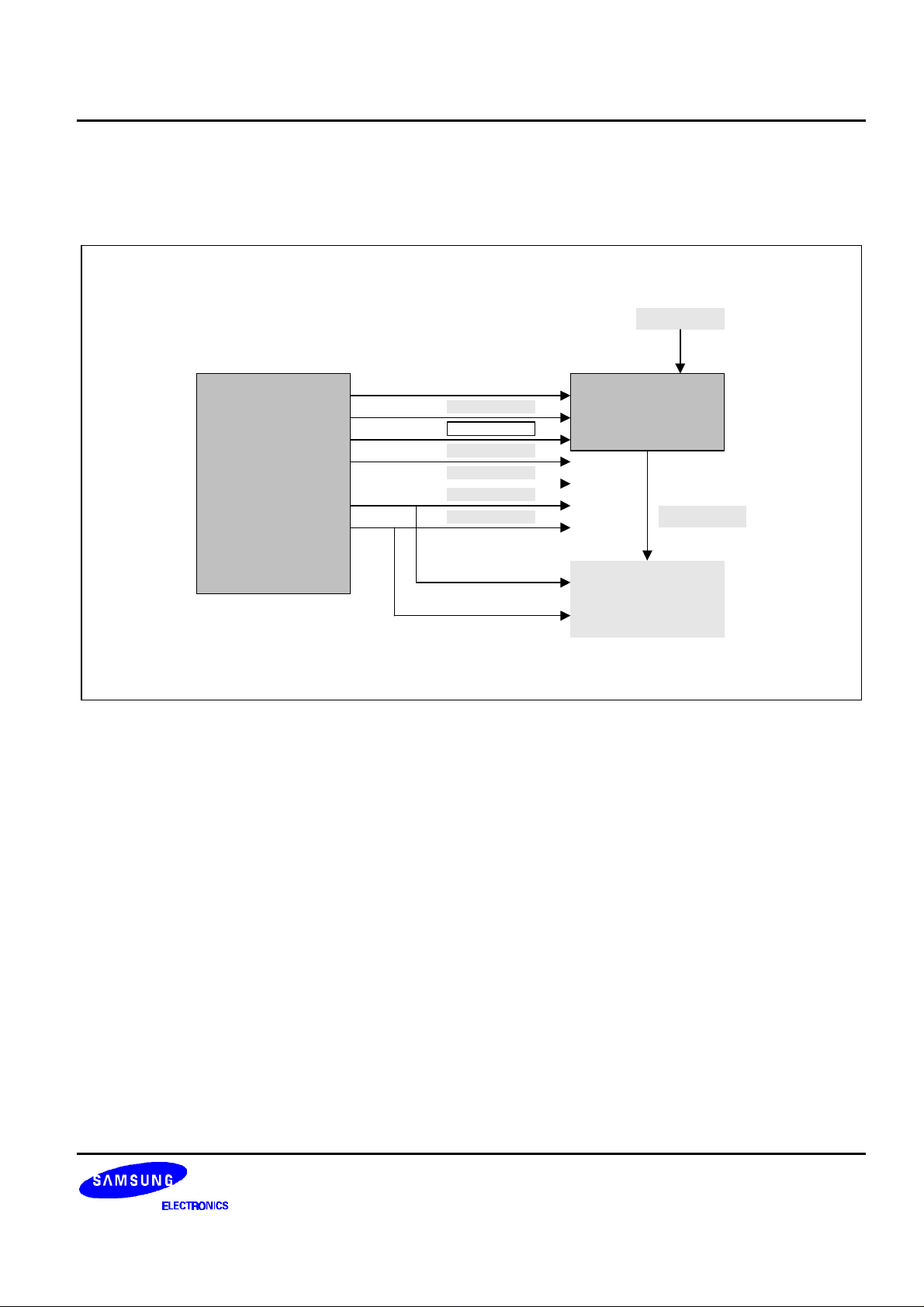
1.1 SYSTEM BLOCK DIAGRAM
CKIN
VOCODER
RESB
SCL
SDA
DIN
FS
MCLK
VIP
DOUT
VOICE
CODEC
1
Page 2
KD16903 DATA PROCESSOR
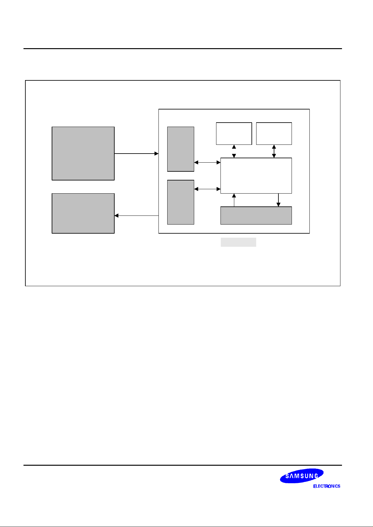
1.2 CHIP BLOCK DIAGRAM
MSM
VOCODER
CODEC
I2C
I/F
Digital
I/F
SRAM
256
VIP
SRAM
256
SSP1611
P.ROM 2K
NOTE: Not Scaled
2
Page 3
DATA PROCESSOR KD16903
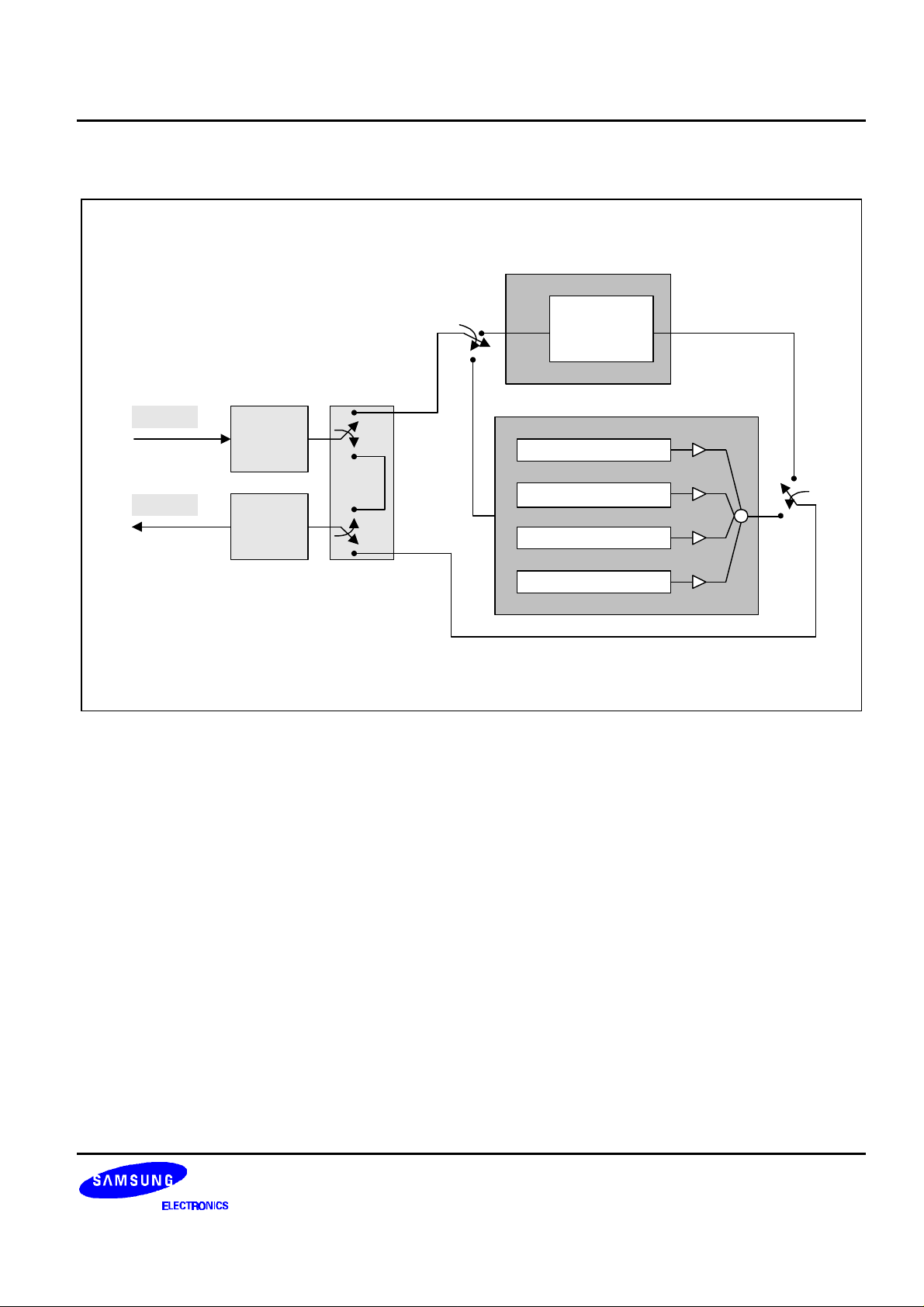
1.3 FUNCTIONAL BLOCK DIAGRAM
Voice
Intelligibility
Proces
DIN
DOUT
PCM
INPUT
I/F
PCM
OUTPUT
I/F
BPF (Center: 300HZ)
BPF (Center: 600HZ)
+
BPF (Center: 1.2kHZ)
HPF (Cutoff: 2.4kHZ)
3
Page 4
KD16903 DATA PROCESSOR
GPO0
VDD1
GPI0
GPI1
GPI2
GPI3
GND1
RESB
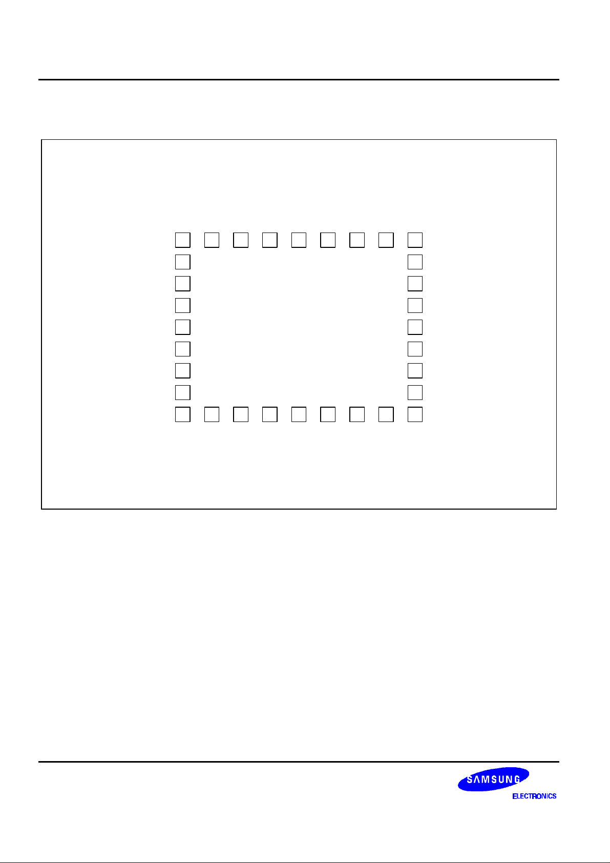
2. PIN ASSIGNMENTS
TCLKDR
TIDR
TSHFTDR
GND3
TUPDDR
TSELDR1
TSEKDR0
VDD3
SAS
VDD4
TODR
GPO3
GPO2
DOUT
GND4
GPO1
25
24 23 22 21 20 19 18
26
27
28
KA16903
29
30
31
32
1 2 3 4 5 6 7 8 9
32BCC
(Top View)
17
16
15
14
13
12
11
10
SCL
SDA
GND2
CKIN
VDD2
MCLK
DIN
FS
4
Page 5
DATA PROCESSOR KD16903
3. PIN DESCRIPTION
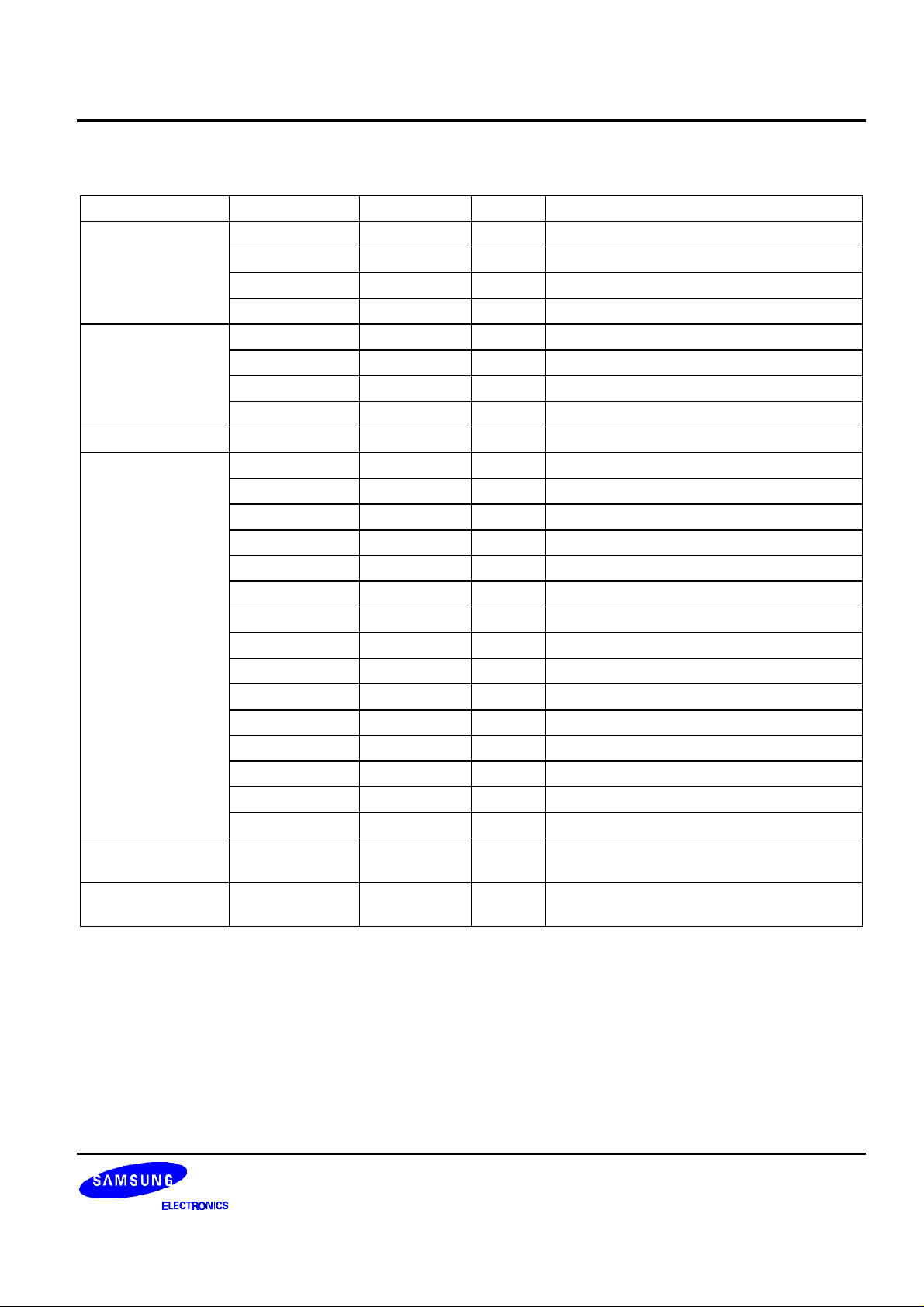
Related Block PIN NAME PIN NO. I/O Description
RESB 8 I Reset: Active Low with CKIN(Min 10 cycle)
HIU SDA 15 I/O I2C Serial Data
SCL 16 I I2C Serial Clock
SAS 17 I I2C Address Selection
DIN 10 I 16 Bit PCM Serial Data In
CIU DOUT 30 O 16 Bit PCM Serial Data Out
FS 9 I PCM Data Frame Sync.
MCLK 11 I PCM Data Bit Clock
System CKIN 13 I System Clock (9.84MHz)
GPI0 3 I Test Pin0 (Host INT. Indicator)
GPI1 4 I Test Pin1(0:No Fade, 1:Fade)
GPI2 5 I Test Pin2 (0:RAM Test)
GPI3 6 I Test Pin3 (0:Codec Bypass)
TSELDR0 19 I Test Pin for JTAG
TSELDR1 20 I Test Pin for JTAG
TEST TUPDDR 21 I Test Pin for JTAG
TSHFTDR 23 I Test Pin for JTAG
TIDR 24 I Test Pin for JTAG
TCLKDR 25 I Test Pin for JTAG
TODR 27 O Test Pin for JTAG
GPO0 1 O Host Ack. Pin
GPO1 32 O Host Test Output
GPO2 29 O Host Test Output
GPO3 28 O Host Test Output
Power VDD1, VDD2
VDD3, VDD4
Ground GND1, GND2
GND3, GND4
2, 12,
18, 26
7, 14,
22, 31
P Digital Power (+3.0V)
G Digital GND
5
Page 6
KD16903 DATA PROCESSOR
~
~
4. DSP PORT ASSIGNMENT FOR I/F WITH PERIPHERALS
I/F Read/ Write Port Interrupt
HIU Read EXT1
INT1
Write EXT1
CIU Read EXT0
INT0
Write EXT0
5. HARDWARE SPECIFICATION
5.1 CODEC INTERFACE UNIT (CIU)
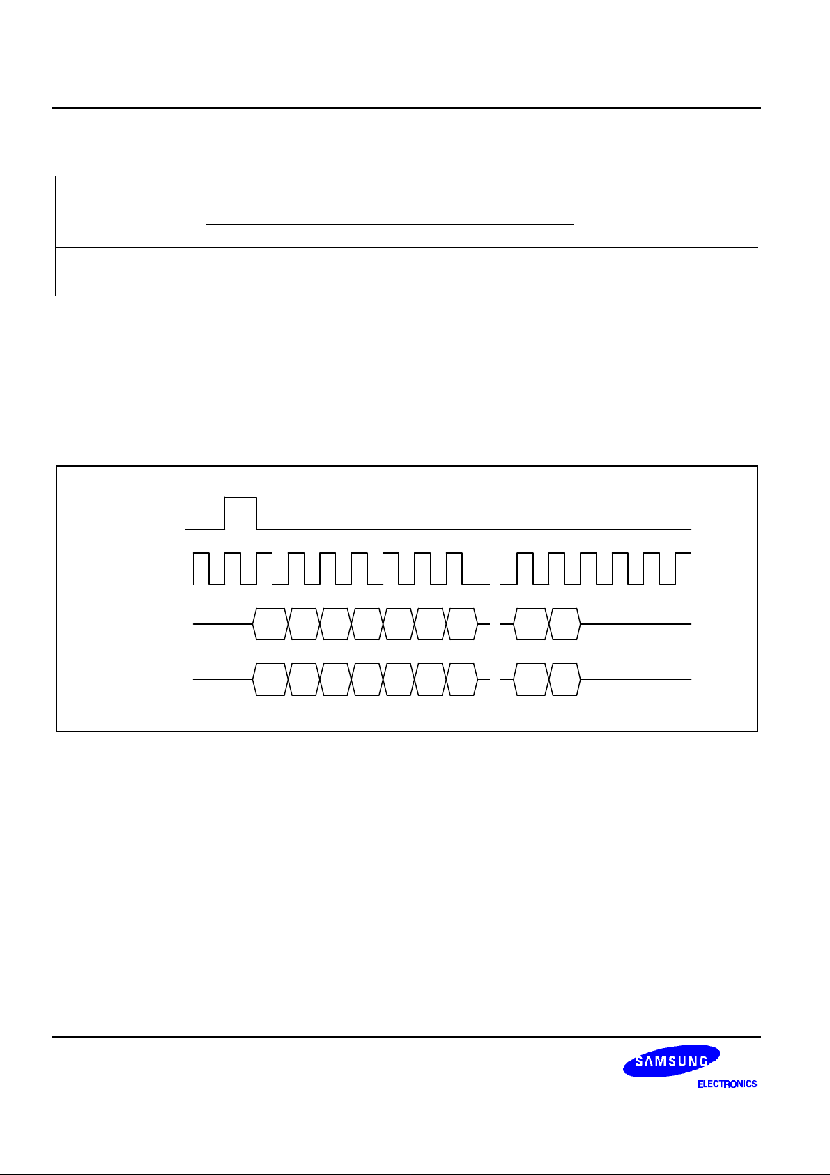
- Time Diagram
FS
MCLK
~
~
DIN
DOUT
1 2 3 4 5 6 15 16
1 2 3 4 5 6 7
7
~
~
15 16
Important!:
During FS (Frame Sync. Clock) high, the falling edge of MCLK (PCM Bit Clock) should exist one time.
6
Page 7
DATA PROCESSOR KD16903
5.2 HOST INTERFACE UNIT (HIU)
- I2C Bus Interface
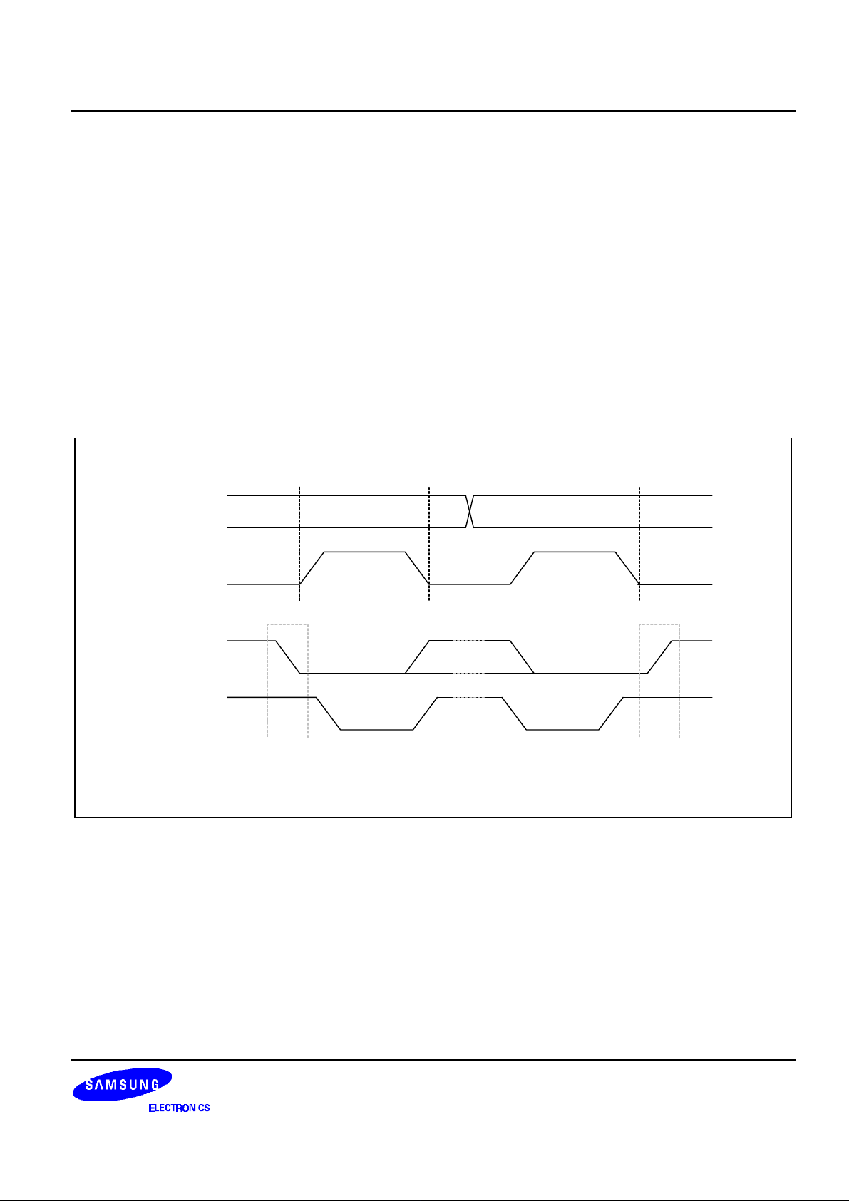
The VIP can be controlled by a microcontroller via the 2-line I2C bus, SDA (Serial Data Line) and SCL (Serial
Clock Line). Both lines must be connected to a positive supply via pull-up resistor. Data transfer may be initiated
only when the bus is not busy. When the bus is free, both lines are high. The data on the SDA line must be stable
during the high period of clock, SCL. When the SCL is low, the SDA can change. Every byte transferred through
the SDA line must contain 8 bits including programmable slave address and read/write direction control bit. Each
byte must be followed by acknowledge bit which is sent back to the microcontroller by the VIP by pulling down the
SDA line. The MSB is transferred first.
- I2C bus interface start and stop condition
The start condition is high to low transition of the SDA line while the SCL is high. The stop condition is low to high
transition of the SDA line while SCL is high.
SDA
SCL
SDA
SCL
Data Valid
S P
Change
of data
Allowed
Start
Condition
Stop
Condition
7
Page 8
KD16903 DATA PROCESSOR
- I2C Bus Interface Acknowledge
The acknowledge related clock pulse is generated by a microcontroller.
The transmitter releases the SDA line (high) during the acknowledge clock pulse. The receiver must pull down
the SDA line during the acknowledge clock pulse so that it remains stable low during the high period of this clock
pulse. The slave-transmitter generates negative acknowledge when read operation processes. The negative
acknowledge is generated by a master (microcontroller).
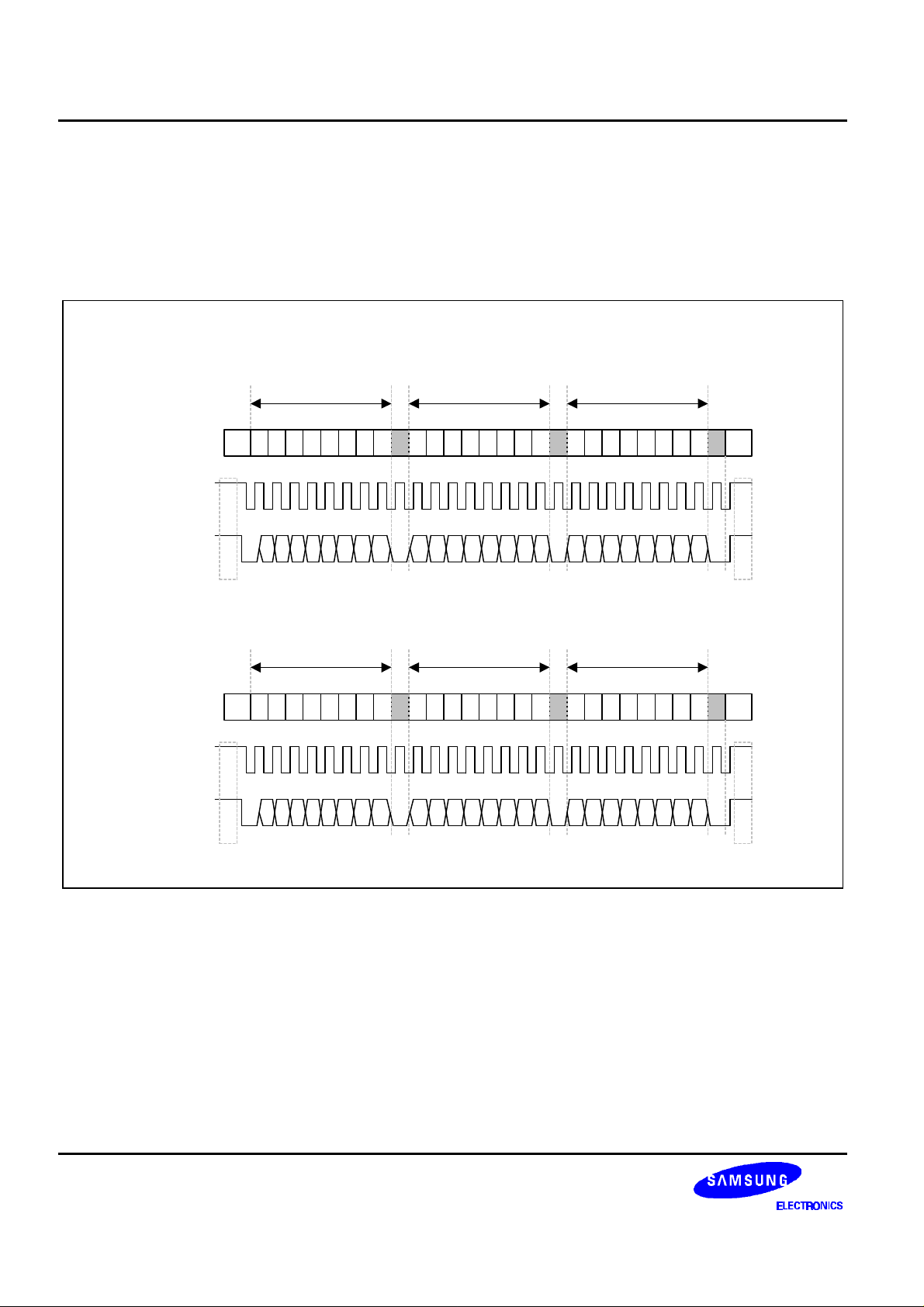
I2C Bus Interface Format-Write Operation
SCL
SDA
SCL
SDA
Chip Address
S 1 0 0 0 0
1 0 0 0 0 0 0 0
S
Chip Address
S 1 0 0 0 0
1 0 0 0 0 0 0 1
S
Function Address
LSBMSB
A0
LSBMSB
AW A A P0
I2C Bus Interface Format-Read Operation
Function Address
LSBMSB
A0
AR A
LSBMSB
DATA
DATA
LSBMSB
P
LSBMSB
N/
P0
A
P
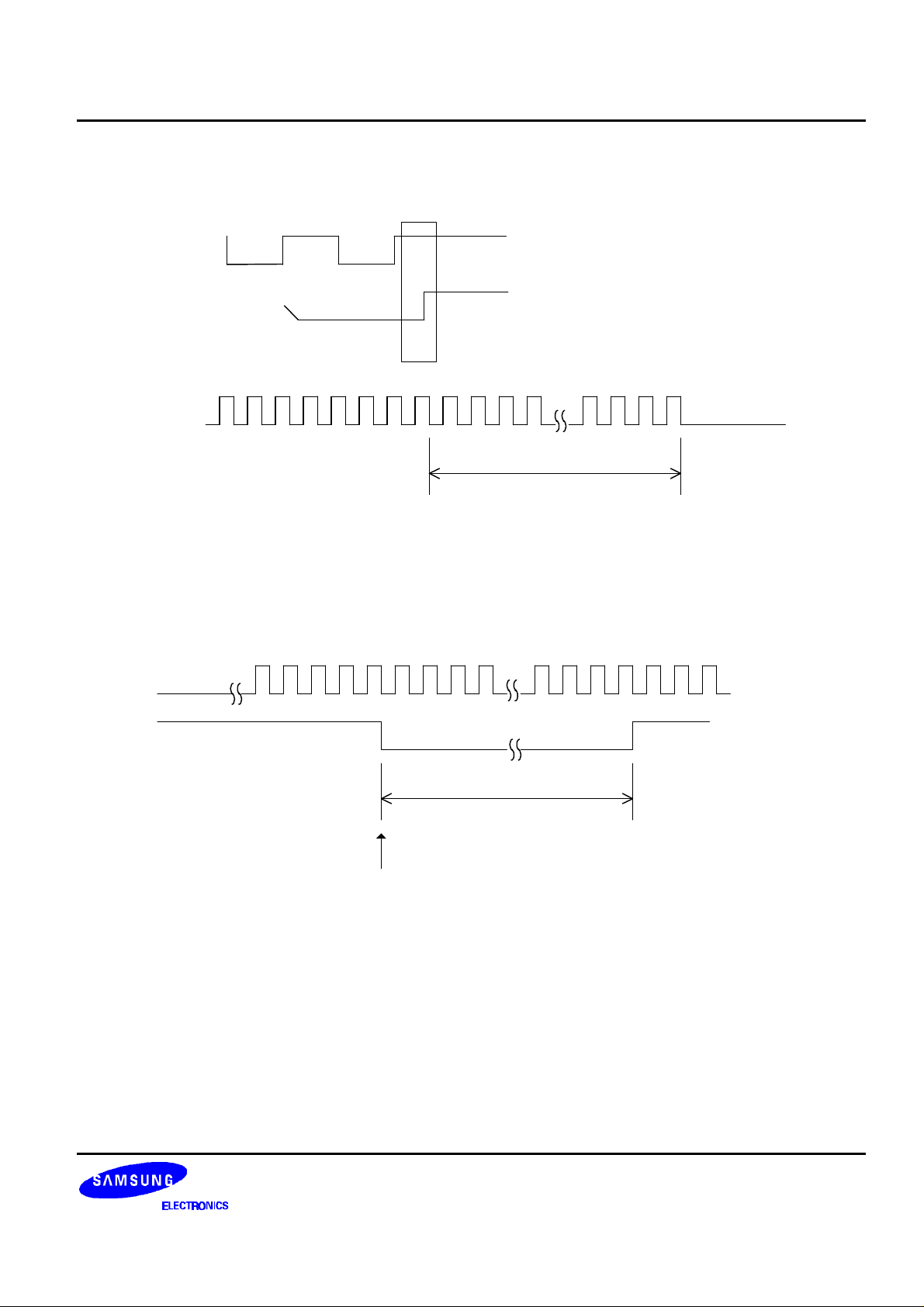
- Relationship between the I2C Bus Interface signal SCL/SDA and main clock of KD16903(CKIN)
Commands are sent from MSM to KD16903 via the I2C (SDA/SCL) bus, triggered by the input signal CKIN. To
achieve immunity towards noise, the glitch protection circuitry must be put into operation, thereby meeting the
I2C specification.
Thus CKIN should be input with the SDA/SCL.
Another issue is, at least 100 clock(CKIN) cycles are needed to execute the command completely by the
KD16903. Even as the end condition of the I2C interface is met, the MSM must supply KD16903 with CKIN, as
8
Page 9
DATA PROCESSOR KD16903
long as the command is being processed.
SCL
SDA
STOP Condition
CKIN
more than 100 clock cycles
RESET Mechanism
RESB should be held "LOW" for more than 10 cycles.
CKIN
RESB
more than 10 clock cycles
CKIN becomes valid at this point
Using RESB
The KD16903 consists of an DSP Unit, Host Interface, and a Codec Interface. And between these internal units,
information is exchanged via the interrupt mechanism.
None of the internally exchanged informations are available outside the KD16903.
On the handphone, signals FS, MCLK, CKIN are controlable by the MSM. However, it is also likely that the
KD16903 may fall into a state of deadlock, since none of these signals are monitorable externally.
9
Page 10

KD16903 DATA PROCESSOR
Furthermore trying to escape from the deadlock state by resupplying the FSK, MCLK, CKIN may not guarantee
nominal operation.
One way to escape from this deadlock state is to use the external reset mechanism. However, it is a good
practice using the internal reset mechanism, supplied at a every new CKIN set, hence avoiding this deadlock
state altogether.
To avoid deadlock, Rest must be used for following three cases.
1. Initialization to enter stable state of KD16903.
2. When changing CKIN(CHIPX8) from Hold to Running.
3. When start running Vocoder.
Please note that the corresponding commands for the functions (VIP/EQ) must be downloaded after the Reset.
- Hardware Recommendation for Reset
Separate GPIO port must be assigned for RESB.
10
Page 11
DATA PROCESSOR KD16903
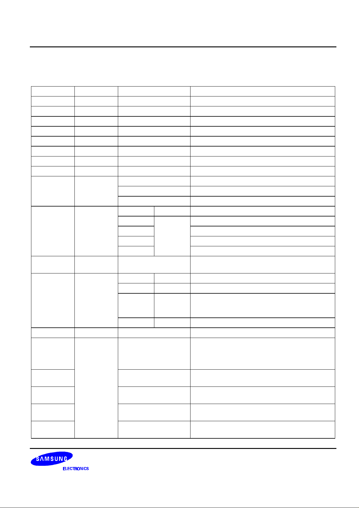
6. COMMAND
6.1 SUMMARY
IC Address Command Data Description
80H 01H - Bypass (Default, DSP OFF)
80H 02H - VIP
80H 03H - Equalizer
80H 04H - Equalizer Flat
80H 05H - Equalizer Mode1
80H 06H - Equalizer Mode2
80H 07H - Equalizer Mode3
80H 08H - Equalizer Mode4
00H VIP Level 100%
80H 09H 01H VIP Level 80%
02H VIP Level 60%
Bit[7:5] Bit[4:0]
000B Band1 Gain Control
80H 0AH 001B 00000H - Band2 Gain Control
010B 11000H Band3 Gain Control
011B Band4 Gain Control
80H 0BH * * H Host Test Mode (Return **H).
Read after IC Read Address 0x81
Bit [7:4] Bit [3:0]
0H 0H - CH VIP Filter1 Gain Control
80H 0CH
...
9H 0H - CH VIP Filter10 Gain Control
80H 0DH 00H - FFH Noise Level Selection
80H 01H Return Current Status followed by IC Read Address
80H 01H Return Band1 Tone Level Status followed by IC
80H 0EH 02H Return Band2 Tone Level Status followed by IC
80H 03H Return Band3 Tone Level Status followed by IC
80H 04H Return Band4 Tone Level Status followed by IC
0H - CH
Bit [3:0] = 0H: +12dB,
Bit [3:0] = CH: 0dB,
1dB Step
0x81, [7:4] = Unused, [3:2] = VIP Level,
[1] = Working Mode(0:VIP, 1:EQ), [0] = Bypass
Flag (0: DSP ON, 1: DSP OFF)
Read Address 0x81 (00H: -12dB - 18H: + 12dB)
Read Address 0x81
Read Address 0x81
Read Address 0x81
11
Page 12
KD16903 DATA PROCESSOR
6.2 DESCRIPTION
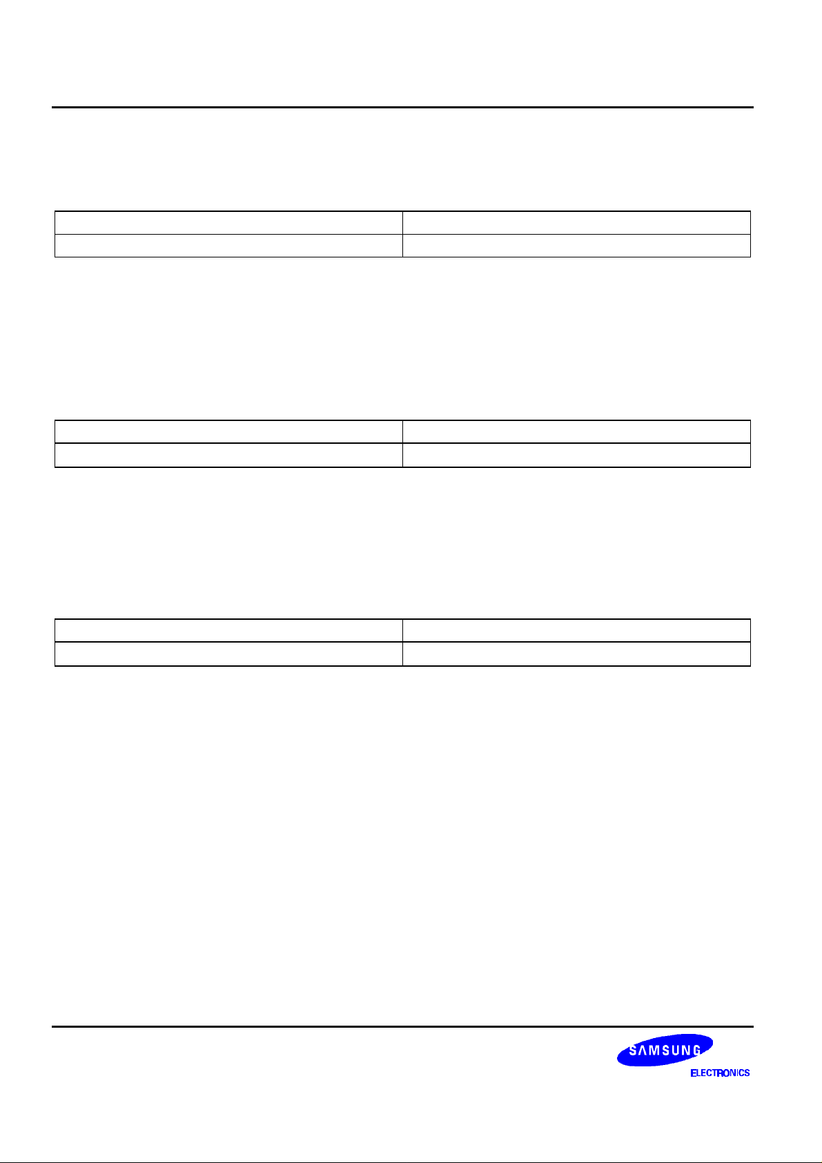
- Bypass Mode
•
Format
Command Code (Hex) Command Name
01 Bypass
• Description
In bypass mode, DIN (PCM input data line) is directly connected to DOUT (PCM output data line) and the DSP is
in stop mode.
- VIP Mode
•
Format
Command Code (Hex) Command Name
02 VIP
•
Description
This one byte command selects VIP mode.
- Equalizer Mode
•
Format
Command Code (Hex) Command Name
03 EQ
•
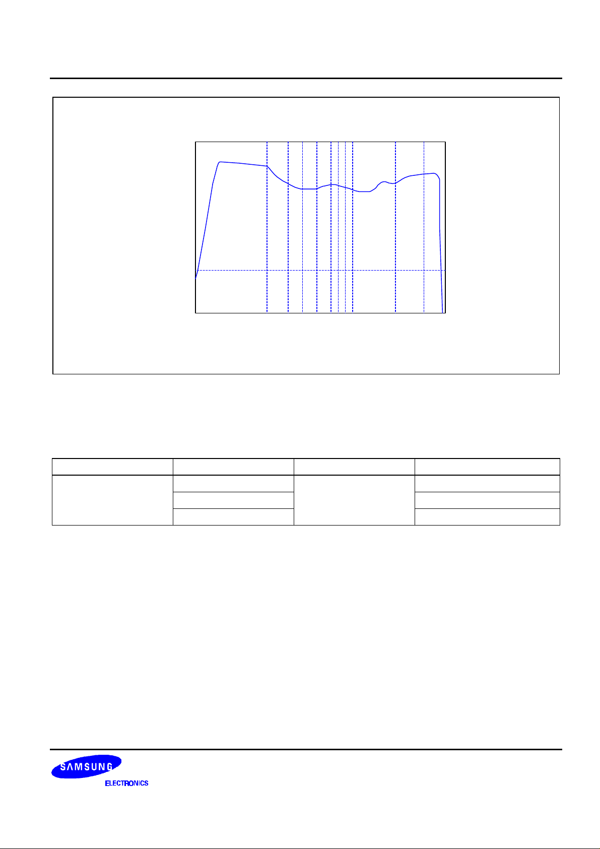
Description
This one byte command selects Equalizer mode. Default tone levels are dipicted in
12
Page 13
DATA PROCESSOR KD16903
10
0
-10
-20
-30
10
2
10
3
Figure 1: Default Tone Level (Band1: + 4dB, Band2: 0dB, Band3: 0dB, Band4: +1dB)
- VIP Level Select
• Format
Command Code (Hex)
00 100% (Max.)
Data (Hex) Command Name Description
09 01 VIP Level 80% (Mid.)
02 60% (Min.)
•
Description
When the current mode is the VIP, its level can be changed using incoming data byte after the command. The
default VIP level is 80%.
13
Page 14
KD16903 DATA PROCESSOR
- EQ Mode Select
•
Format
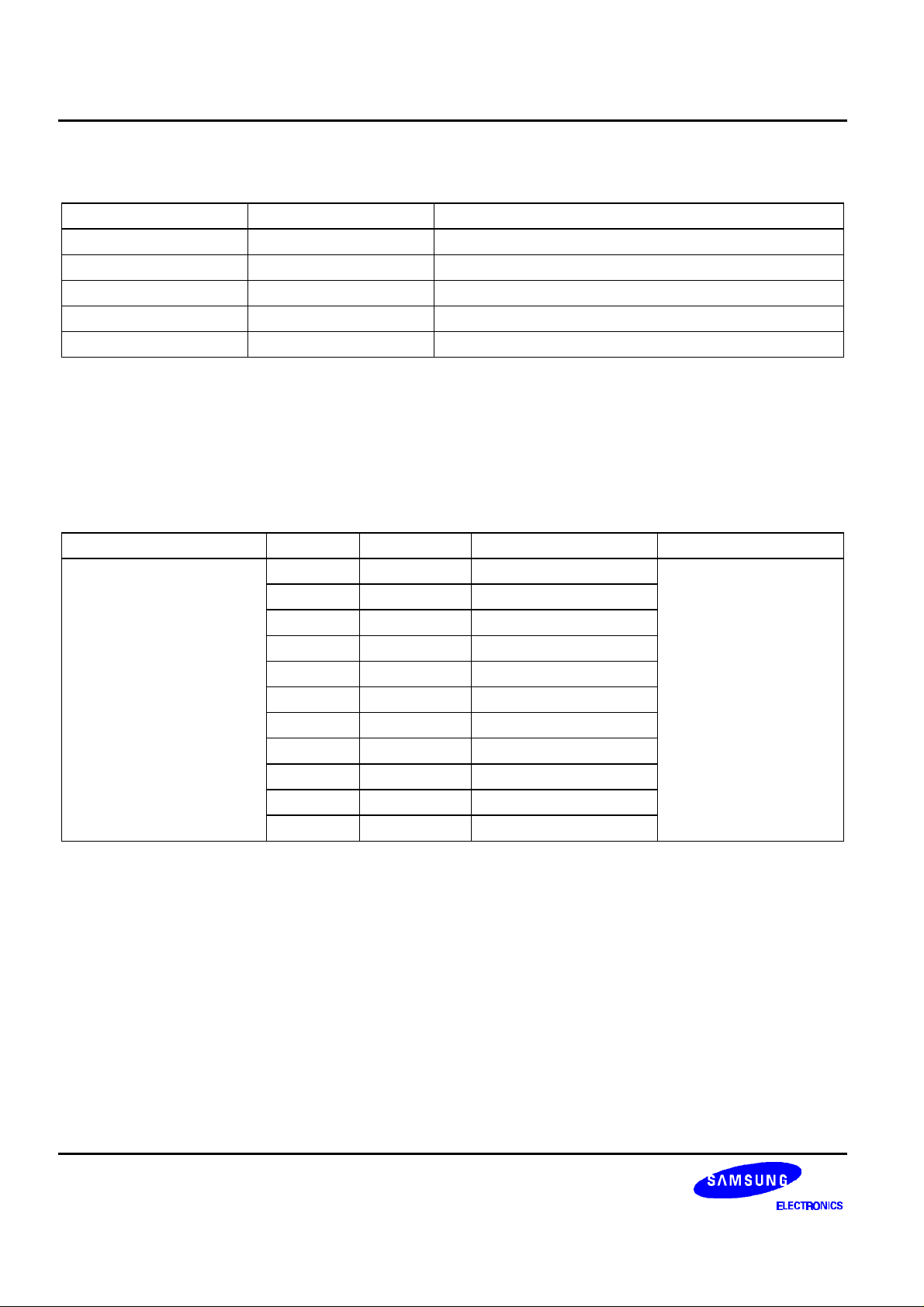
Command Code (Hex)
04 EQ Flat All Bands are set to 0dB
Command Name Description
05 EQ Mode1 Band1: +3dB, Band2: -1dB, Band3: -1dB, Band4: +1dB
06 EQ Mode2 Band1: +3dB, Band2: 0dB, Band3: 0dB, Band4: +3dB
07 EQ Mode3 Band1: +5dB, Band2: 0dB, Band3: 0dB, Band4: 0dB
08 EQ Mode4 Band1: +5dB, Band2: 0dB, Band3: 0dB, Band4: +1dB
•
Description
Although equalizer can control all four bands, it assigns five preset tone level modes.
- EQ Tone Select
• Format
Command Code (Hex) Data Description Command Name
[7:5] 00 Band1 Select
01 Band2 Select
10 Band3 Select
11 Band4 Select
[4:0] 00000 +12dB
0A 00001 +11dB Tone Control
…
01100 0dB
…
10111 -11dB
11000 -12dB
•
Description
The equalizer controls four different frequency bands. The gain for each frequency band can be controlled
between -12dB and +12dB. The [7:5] in data byte after the command determines the frequency band to be
controlled and [4:0] determines gain level.
14
Page 15
DATA PROCESSOR KD16903
- VIP Filter Gain Selection
•
Format
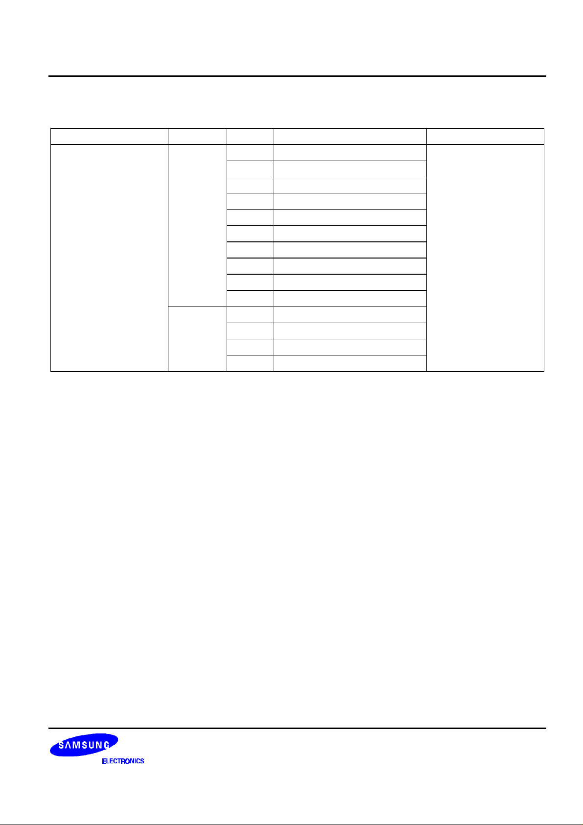
Command Code (Hex) Data (Hex)
0 150Hz Filter Gain to Servo
Description Command Name
1 300Hz Filter Gain to Servo
2 150Hz & 300 Hz Sum Gain
3 600Hz Filter Gain to Servo
[7:4] 4 1.2kHz Filter Gain to Summer
5 1.2kHz Filter Gain to Servo
0B 6 2.4kHz Filter Gain to Summer VIP Filter Gain Control
7 2.4kHz Filter Gain to Servo
8 4.8kHz Filter Gain to Summer
9 4.8kHz Filter Gain to Servo
0 + 12dB
[3:0] 1 + 11dB
…
C 0dB
•
Description
These commands select the gains of filter outputs in the VIP mode. The detailed description of filter structure can
be found in "VIP specification" published by SRS Labs.
15
Page 16
KD16903 DATA PROCESSOR
- Noise Level Selection
•
Format
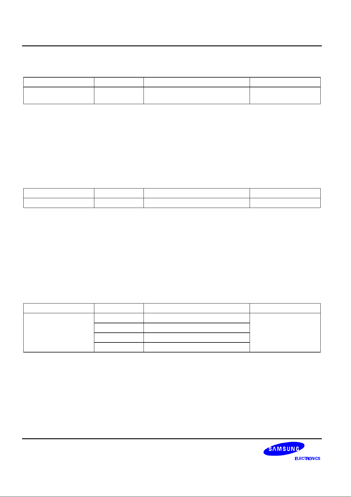
Command Code (Hex)
0D 00 - FF Assume the value in data as noise
Data (Hex) Description Command Name
Noise Level Select
level
•
Description
When the input from ADC has small noise, this noise can incresed in VIP or EQ mode since the specific
frequency levels are increased. To avoid this problem in mute, the input data is tested for 25ms. If the absolute
values of input data are less than noise level specified in Data and stay for 25ms, then the input is considered as
zeros and are processed. Default noise level is set to 0x1F.
- Current Status
•
Format
Command Code (Hex)
0E 01 Return current status register contents Current Status
Data (Hex) Description Command Name
•
Description
It returns the contents of the current status register as:
Status [7:4] = unused
Status [3:2] = VIP Level (00: 100%, 01: 80%, 10: 60%)
Status [1] = Working Mode (0: VIP, 1:EQ)
Status [0] = DSP On/Off (0: DSP On, 1: DSP Off)
- EQ Tone Level Status
•
Format
Command Code (Hex)
02 Return current band1 tone level
Data (Hex) Description Command Name
0E 03 Return current band2 tone level Current Tone Level
04 Return current band3 tone level Status
05 Return current band4 tone level
•
Description
These commands return the current tone levels in EQ mode. Returned byte value is between 0x00 (-12dB) and
0x18 (+12dB).
16
Page 17
DATA PROCESSOR KD16903
7. MEMORY SIZE AND REQUIRED MIPS
7.1 MEMORY SIZE
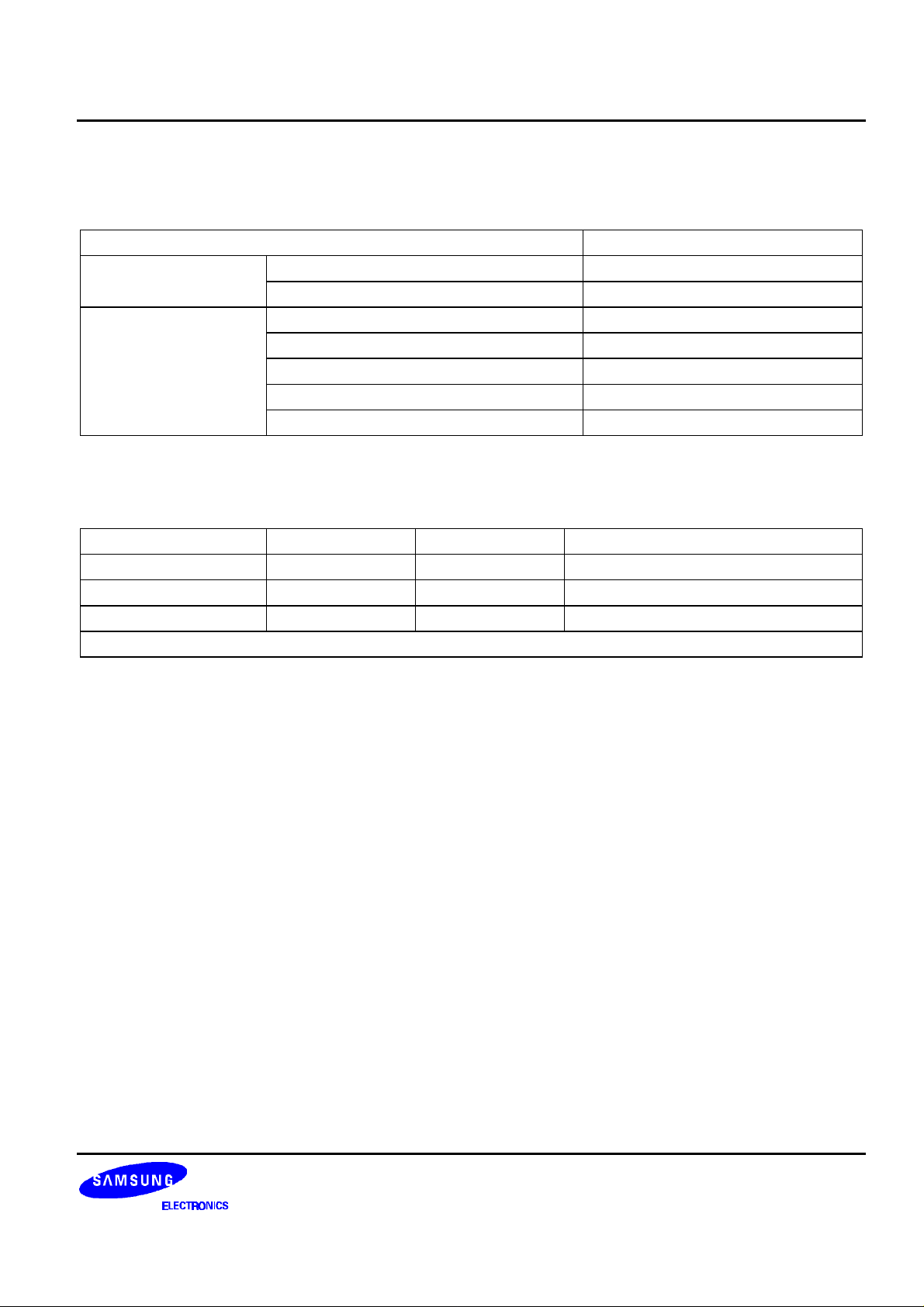
Memory Size (word*)
Data Bank 0 256
Bank 1 256
VIP 800
4band EQ 500
Program Test 400
Others 100
Total 1860
* word = 16 bit
7.2 MIPS
Routines No. of Cycles MIPS Remark
VIP 650 5.2 -
4band EQ 400 3.2 Working only when VIP is OFF
Others 80 0.64 -
Total (VIP ON) = 650 + 70 + 80 = 800 (6.4 MIPS)
17
Page 18
KD16903 DATA PROCESSOR
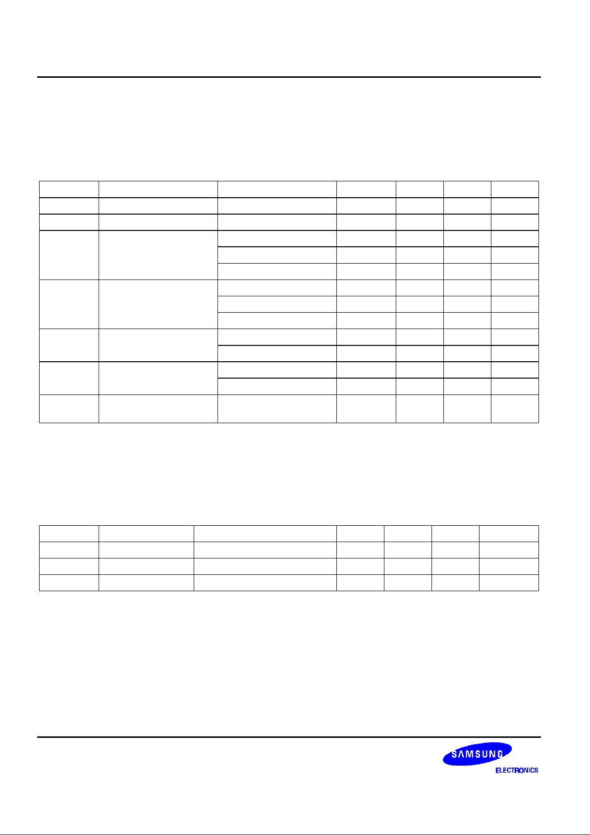
8. ELECTRICAL CHARACTERISTICS
(Unless otherwise specified, Vcc = 2.7V to 3.3V, TA = -30°C to 85°C ; typical characteristic are specified at
Vcc = 3.0V, TA = 25°C; all signals are referenced to GND)
8.1 DIGITAL INTERFACES
Symbol Parameter Test Condition Min. Typ. Max. Unit
VIL Input Low Voltage
VIH Input High Voltage
IOL = 1uA
VOL Output Low Voltage IOL = 4mA (see Note1)
IOL = 8mA (see Note 2)
0.8
IOH = -1uA VDD-0.05
VOH Output High Voltage IOH = -4mA (see Note1) 2.4
IOH = -8mA (see Note2)
IIL Input Low Current VIN = Vss -10
VIN = VSS (see Note3) -60 -30 -10 uA
IIH Input High Current VIN = VDD -10
IOZ Output Current in High
VIN = VDD (see Note4) 60 30 10 uA
VOUT = VSS or VDD -5
impedance (Tri-state)
1.9 V
0.05 V
0.4 V
10 uA
10 uA
5 uA
V
V
V
NOTES:
1. Normal Output Pin
2. SDA ,SCL Output Pin
3. Input Buffer with pull -up (3, 4, 5, 6, 8 Pin)
4. Input Buffer with pull -down (17, 19, 20, 21, 23, 24, 25 Pin)
8.2 POWER DISSIPATION (@3.3V)
Symbol Parameter Test Condition Min. Typ. Max. Unit
ICC0 Operation Current VIP or EQ Operation Mode - 3 4 mA
ICC1 Bypass Current Bypass Operation Mode - 100 150 uA
ICC2 Static Current No Operation (Sleep Mode) - 10 uA
18
Page 19
DATA PROCESSOR KD16903
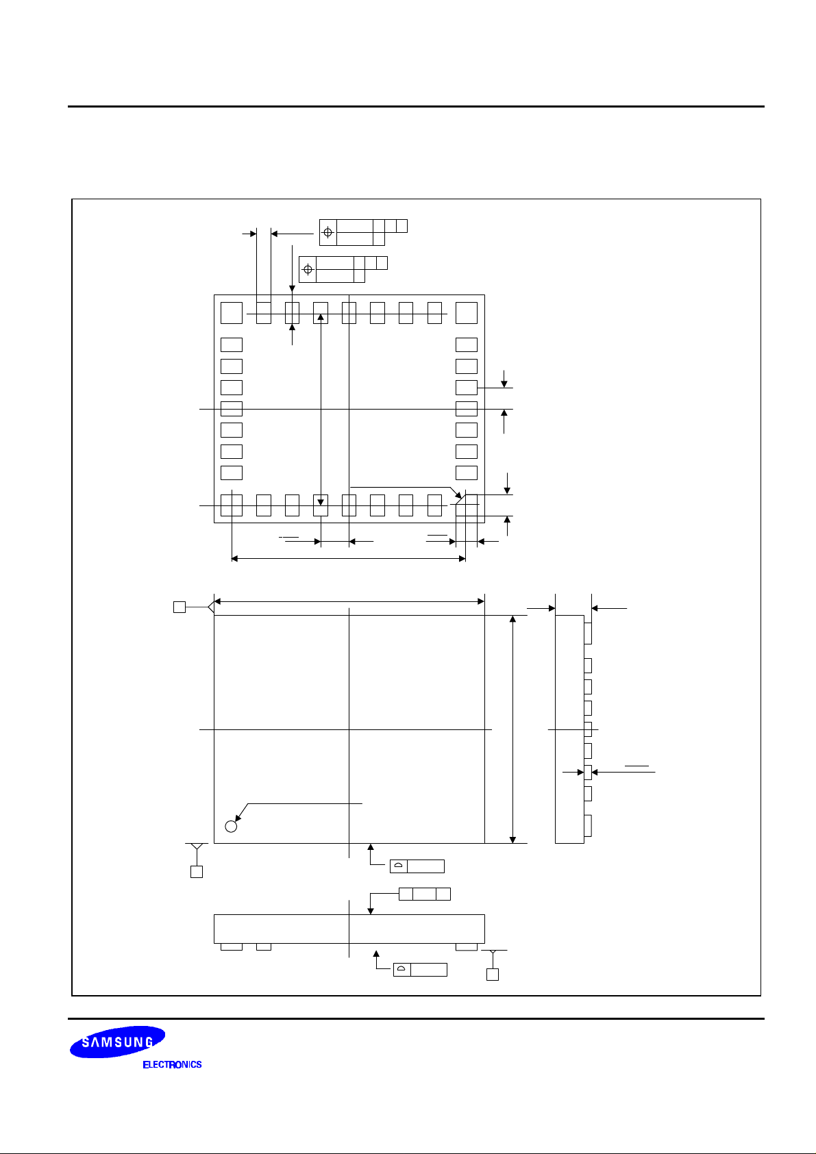
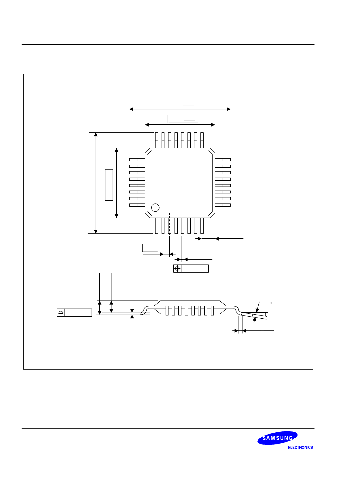
9. PACKAGE DIMENSION
9.1 32 BCC TYPE
0.15
0.03CC
0.15
0.03CC
0.40 + 0.10
4.20
0.50 + 0.10
4.15
B
A B
A B
0.50 + 0.10
PIN CD.2
0.50 + 0.10
0.45 + 0.10
0.60 MAX
5.00 + 0.10
0.75 + 0.025
INDEX
???? MARKING TYPES
4X
A
0.15
/ / 0.20 C
0.15
C
19
Page 20
KD16903 DATA PROCESSOR
0.05 MIN
9.00 + 0.30
7.00 + 0.20
0.10 MAX
9.00 + 0.30
7.00 + 0.20
#32
1.40 + 0.10
170 MAX
0.80
#1
0.30 + 0.10
0.10 MAX
(0.70)
0.127
+ 0.10
- 0.05
0-8
0.50 + 0.20
20
 Loading...