

Page 1
_________________________________________________________________________________________
KC778B Rev C, 1996
KC778B
Master PIR Control Chip (MPCC)
Specification
___________________________________________________________________________
General :
The MPCC has been designed for easy implementation
of AC control functions that use a Passive Infra-Red
(PIR) motion detector. Due to its high sensitivity and
reliability, it is also widely used in security product.
• Minimum external component
• High senstivity
• High RFI immunity
• Daylight adjustment
• Off delay timer
Features:
A) Circuit design maximizes performance while minimizing external component count and board layout space.
B) Low cost solution for PIR motion control switching applications.
C) High sensitivity PIR input with special noise cancellation circuitry.
D) Choice of two PIR gain settings: 62 db and 68 db.
E) Adjustable PIR sensitivity.
F) Internal switched capacitor bandpass filter reduces external component count and improves reliability by
minimizing sensitivity to external component values.
G) RFI noise immunity exceeds 30 V/m from 1 MHz to 1000 MHz.
H) High immunity to line frequency noise.
I) Daylight detector circuitry is designed to use either silicon photo diode or CdS detector.
J) Adjustable daylight detector sensitivity.
K) Adjustable OFF timer accuracy is determined by external components.
L) Output can directly drive TRIACs, opto-couplers and small relays (no buffering required).
M) Four main operating modes can be used in any combination:
1)Auto-ON: Load turns on when motion is detected (adjustable sensitivity).
Adjustable daylight detector disables Auto-ON during daytime.
Auto-ON mode can be disabled.
Daylight detector can be disabled.
2)Auto-OFF: Adjustable OFF timer activates whenever motion stops.
Load turns off if there is no motion during the time delay.
If Auto-ON mode is disabled, the load will turn on if there is motion within 6 seconds
after turn-off. (If the load goes off because you stopped moving (reading a book for
example), you have 6 seconds to wave your arm to turn the load back on.)
Auto-OFF mode can be disabled.
3)Manual-ON: Load turns on manually, with a momentary contact switch.
4)Manual-OFF: Load turns off manually, with a momentary contact switch.
Load will remain off for 25 seconds, even if there is motion during this time (to give you
time to leave the room).
N) If the ON/AUTO/OFF input is held either high or low, the load will be held ON or OFF respectively,
overriding all other modes, until the input returns to the AUTO position.
O) If the Toggle input is held low, the load will change from on to off or from off to on, and will be held in
that state, overriding all other modes, until the input returns high.
P) When power is restored after an outage, the load will be OFF and motion will be ignored for 25 seconds.
Q) Operating chip voltage is 4 - 15V.
R) Operating chip current is typically 300 µA.
S) Chip is ESD protected to more than 1000 V (human body model).
T) Operates with 50-60 Hz AC line frequency.
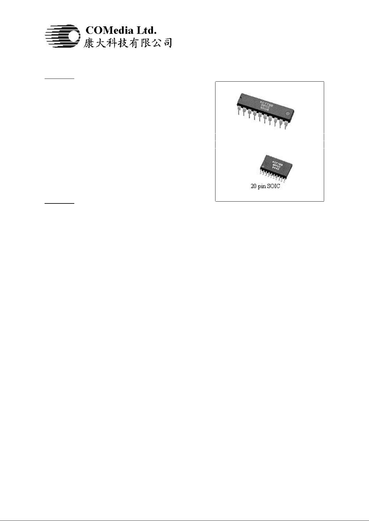
20 pin DIP
Page 2
_________________________________________________________________________________________
2 KC778B
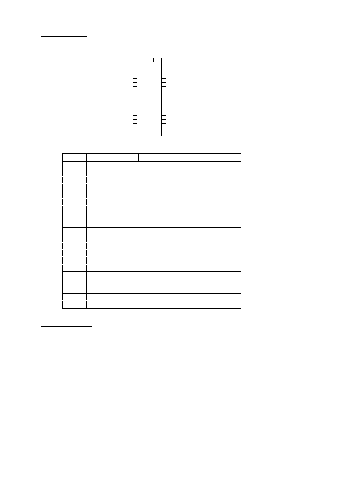
Pin Assignment :
Pin Descriptions
1. Vcc : This is the regulated supply voltage to the chip (nominally 5 V).
2. Sensitivity Adjust: This pin is used to adjust the sensitivity threshold of the motion comparators. When the
voltage on this pin equals the pyro drain reference voltage on pin 7 the PIR sensitivity will be minimum
(±500 mV). When the voltage on this pin is Gnd the PIR sensitivity will be maximum (±125 mV).
Intermediate voltages will provide intermediate sensitivities.
3. Offset Filter: This pin connects to an external capacitor of 10 µF and holds the average value of the
switched capacitor bandpass filter output. Motion is detected when the difference between this average and
the actual filter output is greater than the sensitivity setting. The output of the switched capacitor bandpass
filter can be seen directly on this pin if the external capacitor is disconnected, however, motion will not be
detected under these conditions.
4. Anti-Alias: This pin connects to an external capacitor of 0.1 µF providing low pass filtering of the PIR
input signal, blocking input signals at and above the switching frequency of the switched capacitor
bandpass filter.
1 20
2 19
3 18
4 17
5 16
6 15
7 14
8 13
9 12
10 11
20 pin DIP or SOIC
Pin Name Description
1 Vcc Supply Voltage (5 V)
2 Sensitivity Adjust PIR Motion Sensitivity Input
3 Offset Filter PIR Motion Offset Filter
4 Anti-Alias PIR Anti-Alias Filter
5 DC CAP PIR Gain Stabilization Filter
6 VReg Voltage Regulator Output
7 Pyro (D) Pyro Drain Reference
8 Pyro (S) Pyro Source Input Signal
9 Gnd (A) Analog Circuitry Ground
10 Gnd (D) Digital Circuitry Ground
11 Daylight Adjust Daylight Adjustment and CdS Input
12 Daylight Sense Silicon Photo Diode Input
13 Gain Select PIR Gain Select Tri-State Input
14 ON/AUTO/OFF Mode Select Tri-State Input
15 Toggle Mode Select Toggle Input
16 OUT Lights ON/OFF Output
17 LED PIR Motion Indicator Output
18 C OFF Timer Oscillator Input
19 R OFF Timer Oscillator Output
20 FRef Frequency Reference Oscillator
Page 3

_________________________________________________________________________________________
MPCC 3
5. DC CAP: This pin connects to an external capacitor of 10 µF and holds the average pyro source voltage.
The difference between this average and the actual pyro source voltage is amplified and coupled to the
switched capacitor bandpass filter. The 10 µF capacitor must be a low leakage capacitor, such as a
Tantalum capacitor.
6. VReg: This pin outputs a voltage that can be used directly drive an external NPN/PNP volatage regulator,
or the gate of an external depletion mode JFET voltage regulator pass element. This pin need not be
connected if an external voltage regulator, such as a three pin regulator, is used to generate Vcc for the
chip.
7. Pyro (D): The pyro drain reference voltage is output on this pin. This voltage is power supply independent
and is connected internally to special noise cancellation circuitry to improve the performance and reliability
of the PIR interface. Externally, this pin is connected to the pyro drain and to a 0.1 µF capacitor. This
voltage can also be divided down by an external pot to supply the Sensitivity Adjust voltage to pin 2.
8. Pyro (S): This is the pyro source input pin that receives the PIR input signal. It is connected externally to
the pyro source, a 200 pF capacitor and a 47 K
Ω
resistor to Gnd. This is a sensitive node and the length of
the external interconnect to this pin should be made as short as possible. There should be a ground plane
on the PC board under the PIR sensor.
9. Gnd (A): This pin is the electrical ground for the internal analog circuitry of the chip.
10. Gnd (D) : This pin is the electrical ground for the internal digital circuitry of the chip.
11. Daylight Adjust: This pin is the output of the Daylight Sense amplifier and the input to the daylight
comparator. When using a silicon photo diode daylight sensor, this pin is connected to Daylight Sense (pin
12) by a resistor or pot. The amount of resistance determines the gain of the Daylight Sense amplifier and
hence the sensitivity of the daylight detector. When using a CdS daylight sensor, a pot is connected
between this pin and Vcc, while the CdS sensor is connected across one side of the pot (two fixed resistors
can be used instead of the pot). Daylight Sense (pin 12) must be connected to Vcc when using a CdS
sensor. To disable the daylight detector, Daylight Adjust (pin 11) must be unconnected and Daylight Sense
(pin 12) must be connected to Vcc. To disable Auto-ON mode, Daylight Adjust (pin 11) and Daylight
Sense (pin 12) must both be connected to Vcc (the daylight detector is not used when Auto-ON mode is
disabled).
12. Daylight Sense: This pin is the input to the Daylight Sense amplifier. When using a silicon photo diode
daylight sensor, this pin is connected to the cathode of the silicon photo diode and to a feedback resistor (or
pot) from Daylight Adjust (pin 11). In all other cases, this pin is connected to Vcc.
13. Gain Select: The Gain Select pin is a tri-state input used to select the gain of the PIR circuitry. When this
pin is connected to Gnd, the PIR gain is set to 62 db. When this pin is unconnected or connected to Vcc,
the PIR gain is set to 68 db. Normally this pin is unconnected except when less gain is required by a
particular PIR sensor.
14. ON/AUTO/OFF: This pin is a tri-state input used to determine the operation of the chip. Normally this
pin is unconnected, allowing the chip to operate in its configured operating mode. If this pin is connected
to Gnd, the load will turn off unconditionally and will remain off as long as this pin is connected to Gnd. If
this pin is connected to Vcc, the load will turn on unconditionally and will remain on as long as this pin is
connected to Vcc.
15. Toggle: This pin is a toggle input used to determine the operation of the chip. Normally this pin is
unconnected, allowing the chip to operate in its configured operating mode. If this pin is connected to
Gnd, the load will change from on to off or from off to on and will remain in the new state unconditionally
as long as this pin is connected to Gnd. If the ON/AUTO/OFF (pin 14) and Toggle (pin 15) switches are
pressed such that one is trying to turn the load on unconditionally and the other is trying to turn the load off
unconditionally, the load will be turned off (off overrides on).
16. OUT : The output from this pin is used to turn the external load on or off through a TRIAC, relay or opto-
coupler. The impedance of this pin is less than 35
Ω
, enabling it to directly drive a small (100 Ω DC coil
resistance) pulse relay through a 150 µF series capacitor. For proper operation, the load should come on
when this pin goes high, the load should go off when this pin goes low.
Page 4

_________________________________________________________________________________________
4 KC778B
17. LED: The output from the motion comparator drives this pin through an internal 500
Ω
current limiting
resistor, enabling it to directly drive an LED motion indicator. Whenever motion is detected this pin will
go high and the LED will light. When there is no motion this pin will be low.
18. C: This pin is the input to the OFF timer oscillator. It is connected externally to a pot (or resistor) from R
(pin 19) and to a capacitor. The OFF timer delay, in seconds, will be 5678 x (40,000 + pot resistance in
Ohms) x (capacitance in Farads). To disable Auto-OFF mode, this pin can be connected to Gnd or Vcc.
For minimum time delay, C(pin 18) and R(pin 19) can be shorted together with no external resistor or
capacitor. In this configuration, the output at OUT(pin 16) should be the same as the output at LED(pin
17).
19. R : The output of the OFF timer oscillator drives this pin through an internal 40 K
Ω
series resistor. This
pin is connected externally to C (pin 18) through a pot (or resistor). This pin can be connected directly to
C (pin 18) for the minimum OFF timer delay (maximum oscillator frequency).
20. FRef : This is the 160 Hz reference oscillator input. It is connected externally through a 330K
Ω
resistor to
Vcc and a 0.022µF capacitor to Gnd. Other values of resistance and capacitance can be chosen, provided
this input oscillates at 160Hz. This frequency is used to drive the internal switched capacitor bandpass filter
and the timing delays.
Electrical Specifications
Below are the specifications at room temperature (25 °C).
Parameter Min. Typ. Max. Unit
Vcc 4 5 15 V
Icc 300 µA
Input Voltage on any Pins Gnd - 0.5 Vcc + 0.5 V
PIR Power Supply Rejection Ratio 74 dB
PIR Input Gain 62 68 dB
Overall gain variation 5 %
Overall threshold variation 7 %
Daylight Adjust (pin 11) Pull-down Current 5
µA
Gain Select (pin 13) Pull-up Current 5 µA
ON/AUTO/OFF (pin 14) Pull-up Current 10 µA
ON/AUTO/OFF (pin 14) Pull-Down Current
10 µA
Toggle (pin 15) Pull-up Current 5 µA
Pyro (D) (pin 7) Reference Voltage 2.3 2.5 2.7 V
OUT (pin 16) Output Impedance 35
Ω
LED (pin 17) Output Impedance 375 500 625
Ω
R (pin 19) Output Impedance 30 40 50
K
Ω
Operating Temperature -25 +100 °C
Storage Temperature -55 +125 °C
Application Notes:
1. Normally, Gain Select (pin 13) is unconnected, providing a PIR gain of 68 db. For reduced sensitivity, Gain
Select is connected to Gnd, providing a gain of 62 db.
2. Auto-ON mode can be disabled by connecting both Daylight Sense (pin 12) and Daylight Adjust (pin 11) to
Vcc.
3. Auto-OFF mode can be disabled by connecting C (pin 18) to Gnd or Vcc.
4. Daylight detector can be disabled by connecting Daylight Sense (pin 12) to Vcc.
5. With a 5 M
Ω
Daylight adjust pot, the daylight sensitivity can be adjusted from complete darkness (always
on) to complete daylight (always off). Additional fixed resistors and possibly a smaller pot can be used to
restrict the range for specific applications.
6. The OFF timer range can be set by selecting a pot and capacitor and possibly additional fixed resistors that
will produce the minimum and maximum time delays at the extremes of the pot.
Page 5

_________________________________________________________________________________________
MPCC 5
7. OFF timer delay = 5678 x (R+40,000) x C seconds, R is in Ohms, C is in Farads.
8. The Sensitivity Adjust pot is used to select a voltage between the pyro drain reference voltage (minimum
sensitivity) and Gnd (maximum sensitivity). The value of the pot is not critical and any value between 100
K
Ω
and 5 MΩ can be used.
9. The output of the switched capacitor bandpass filter can be seen on pin 3 (Offset Filter) when the external
capacitor(10µF) is disconnected. The filter response can be measured in this way. (Disconnecting the
external capacitor prevents motion from being detected.)
10. Pin 8 (Pyro (S)) is a sensitive node and the external interconnect to this pin should be made as short as
possible. This node should also be closely surrounded by a ground plane.
Block Diagram
VCC
Sensitivity
Adjust
Offset Filter
Pyro (D)
Pyro (S)
Gain Select
Anti-Alias
DC Cap
FRef
R
C
On/Auto/off
Toggle
Daylight
Sense
Daylight
Adjust
GND
PIR Front End
Amplifiers and
Noise Cancellation
Circuitry
Switched
Capacitor
Bandpass Filter
Oscillation and
Synchronization
Circuitry
Threshold
Comparators
and Timing
Circuitry
Daylight Detector
Amplifier and
Comparator
Voltage Regulator
LED
OUT
Vreg
Page 6

_________________________________________________________________________________________
6 KC778B
Application Circuit
1. Typical Hook-up
Below is a typical hook up for connecting KC778B to a PIR sensor, a TRIAC light switch and a silicon
photodiode daylight detector. VReg is used for voltage regulation. 2 slide switches are used. One for select
ON/AUTO/OFF and the other one used for enable, disable the daylight sensor and disable auto-on function.
A simple AC regulation circuit is used in this system such that only a small gate current TRIAC can be
used.
(L)
LIGHT
100
1W
400V
.47uF
470K
X24004
1N
470
8550
10uF 470uF
C9014
12V
.1uF
.01uF
400V
TRIAC
AC
200V
(N)
1K
330K
.022uF
20OSC
1 VCC
KC778B
500K
MAX
MIN
10uF
23PIR
SENS
OFFSET
FILTER
1819C
R
OFF TIMER
R
C
AUTO
TOGGLE ON-OFF
15
16
17
TOGGLE
OUT
LED4
5
6
LP
FILTER
DC
CAP
VREG
10uF
TAN
.1uF
PIR
.1uF
47K
7
8
9
PYRO
PYRO
GND
(D)
(S)
(A)
12
13
14
DAY
SENS
GAIN
ON/OFF
NC
ON
OFF
DISABLE AUTO-ON
DISABLE DAY SENS
20K
5M PHOTO
DIODE
DAY SENSOR11DAY
ADJ
SW 2P3T
10 GND
(D)
200pF
Note : Off Time Delay = 5678 x (R+40,000) x C Second
R in Ohm, C in Farad
Page 7

_________________________________________________________________________________________
MPCC 7
2. Hook-up with with relay
The following is similar to the typical hook-up. Due to the higher current require by relay, the bridge
regulation method is used in AC circuit. This application is suitable to a high current loading such as
heater, flood light, motor and etc.
(L)
100
1W
400VX4
1uF
200
1N4004
470
8550
10uF 470uF
C9014
12V
470K .01uF
400V
(N)
200V AC
100uF
330K
500K
MIN
MAX
12VCC
PIR
SENS
KC778B
1920R
R
OFF TIMER
OSC
C
.022uF
LOAD
RELAY(12VDC)
4001
8050
1K
TOGGLE ON-OFF
16
17
18
OUT
LED
COFFSET
FILTER
LP
FILTER
DC
CAP
3
4
510uF
TAN
.1uF
10uF
PIR
.1uF
6
7
8
PYRO
PYRO
(D)
(S)
VREG
13 NC
14
15
GAIN
ON/OFF
TOGGLE
ON
OFF
AUTO
DISABLE AUTO-ON
20K
5M PHOTO
DIODE
DAY SENSOR
DISABLE DAY SENSE
11
12
DAY
ADJ
DAY
SENS
GND
GND
(A)
(D)
9
10
200pF
47K
SW 2P3T
Note : Off Time Delay = 5678 x (R+40,000) x C Second
R in Ohm, C in Farad
Page 8

_________________________________________________________________________________________
8 KC778B
3. Hook-up with minimun regulator
Below is an example of 110V application. Only one stages of regulator is used in the system by use of
zener diode
LIGHT
(L)
100
1W
400VX2
470K
1uF
4004
1N
220
1N4148
10uF
5.6V
470uF
.1uF .01uF
400V
TRIAC
110v
AC
(N)
.022uF
330KKC778B
500K
MAX
MIN
1
2
310uF
VCC
PIR
SENS
OFFSET
FILTER
18
19
20
C
R
R
OFF TIMER
OSC
C
1K
TOGGLE ON-OFF
15
16
17
TOGGLE
OUT
LEDLP
FILTER
DC
CAP
VREG
4
5
6
10uF
TAN
.1uF
.1uF
PIR
7
8
947K
PYRO
PYRO
GND
(D)
(S)
12
13 NC
14
DAY
GAIN
ON/OFF
ON
OFF
AUTO
DISABLE AUTO-ON
20K
5M PHOTO
DIODE
DAY SENSOR
DISABLE DAY SENS
11DAY
ADJ
SENS
GND
(A)
(D)
10
200pF
SW 2P3T
Note : Off Time Delay = 5678 x (R+40,000) x C Second
R in Ohm, C in Farad
Page 9

_________________________________________________________________________________________
MPCC 9
4. Hook-up with 12VDC system
Below is an example of Auto camp light which uses an auto battery (12VDC). Internal voltage regulator is
used, it needs 12V to start up but can work down to 7V.
C1
470uF
Q1
8550
Q2
9013
C2
220uF
KC778B
R1
330K
C9
223
LP1
LAMP
1920R
OSC
R2
120K
12VCC
PIR
SENS
C3
10uF
D1
1N4001
BT1
12V
C4
104
C5
10uF
34OFFSET
FILTER
LP
FILTER
17
18
LED
C
C8
104
D2
1N4148
K1
RELAY
Q3
8050
R5 1K
R3
20K
S1
MANUAL OVERRIDE
15
16
TOGGLE
OUT56DC
CAP
VREF
TAN
C6
104
PIR
78PYRO
PYRO
(D)
(S)
13
14
GAIN
ON/OFF
R6
100K
CdS
R7
510k
11
12
DAY
ADJ
DAY
SENS
910GND
GND
(A)
(D)
C7
200P
R4
47K
5. Hook-up with Door Chime and Alarm circuit
A 2P3T slide switch is used in the system.When it is positioned at Chime, the LED output of KC778B will
trigger the door bell COB at anytime. If the switch is positioned at OFF, power will be cut off. When switch
to Alarm position, after 25sec delay, the KC778B start working. It outputs a high signal when motion is
detected. This signal will charge up the cap such that the siren COB will be triggered after the charge up
delay time. It forms a very simple alarm product.
SW1
2P3T
CHIME
R1
330K
R5
100
C4
100uF
C5
470uF
D2
IN4148
OFF
ALARM
BT1
6V
C1
223
1
2
3
4
5
6
7
8
9
10 11
12
13
14
15
16
17
18
19
20
U1
KC778B
R2
220K
C2
103
PIEZO
T1
CHOKE
COB
DOOR BELL
TRG
R3
56
D1
1N4148
R4
68K
SW2
2P3T
Q1
8050
SIREN
COB
TRG
C3
100uF
 Loading...