

Page 1
®
KBMFxxSC6
A.S.D.
FOR PS/2 MOUSE OR KEYBOARD PORTS
MAIN APPLICATION
EMI Filter and line termination for mouse and keyboard ports on:
- Desktop computers
- Notebooks
- Workstations
- Servers
DESCRIPTION
On the implementation of computer systems,
theradiatedand conducted EMI should bekept
within the required levels as stated by the FCC
regulations. In addition to the requirements of
EMC compatibility, the computing devices are
required to tolerate ESD events and remain
operational without user intervention.
TheKBMFimplementsa low pass filter to limit EMI
levels and provide ESD protection which exceeds
IEC 61000-4-2 level 4 standard. The device also
implementsthepull up resistors neededtobias the
data and clock lines. The package is the
SOT23-6L which is ideal for situations where
board space is at a premium.
FEATURES
■
Integrated low pass filters for Data and Clock
lines
■
Integrated ESD protection
■
Integrated pull-up resistors
■
Small package size
■
Breakdown voltage: VBR=6Vmin
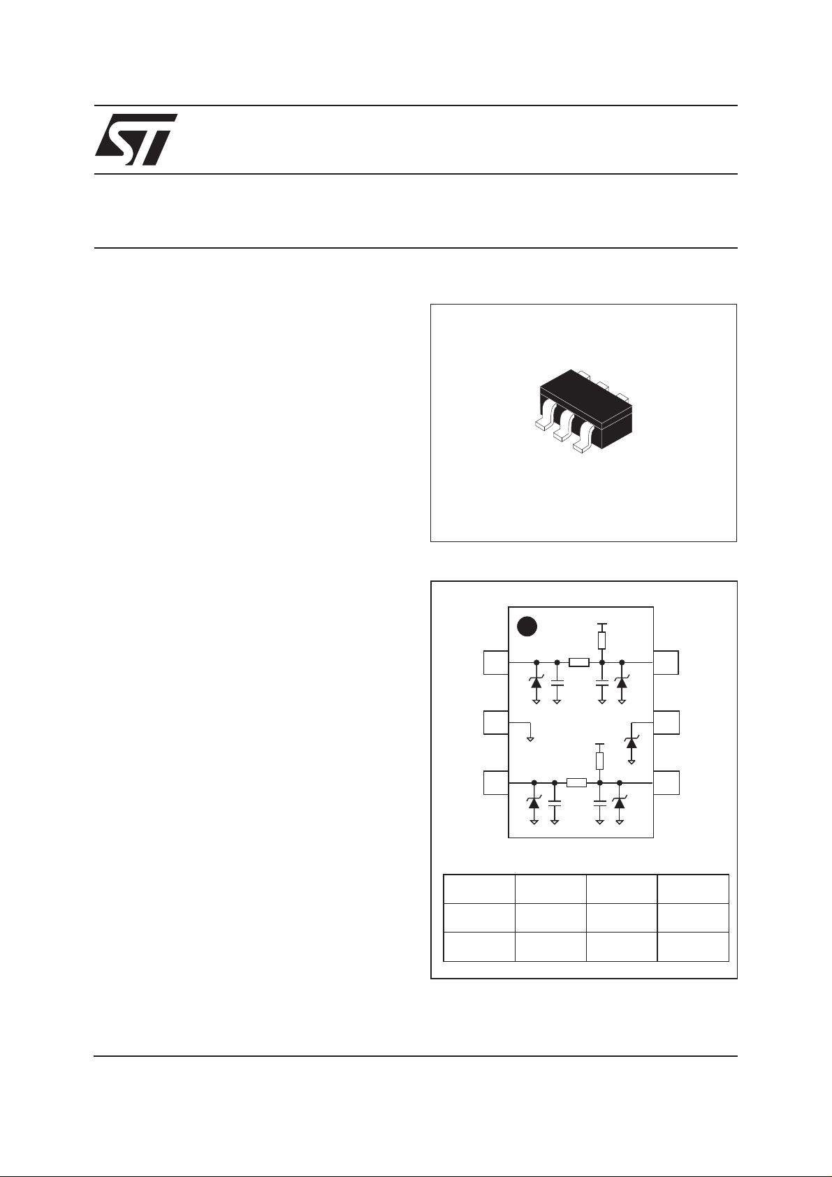
EMI FILTER AND LINE TERMINATION
SOT23-6L
FUNCTIONAL DIAGRAM
Rs
Dat In
CRpC
Gnd
Rs
Clk In
CRpC
+Vcc
Dat Out
+Vcc
+Vcc
Clk Out
BENEFITS
■
EMI / RFI noise suppression
■
ESDprotectionexceeding IEC61000-4-2 level4
■
High flexibility in the design of high density
boards
TM: ASDandTRANSIL are trademarks of STMicroelectronics.
February 2002 - Ed : 1D
Rs Rp C
code 01 39Ω 4.7kΩ 120pF
Tolerance ±10% ±10% ±20%
1/8
Page 2
KBMFxxSC6
COMPLIES WITH THE FOLLOWING ESD
STANDARDS:
IEC 61000-4-2 (R = 330Ω C = 150pF), level 4
±15 kV (air discharge)
±8 kV (contact discharge)
MIL STD 883C, Method 3015-6
Class 3 C = 100 pF R = 1500 Ω
3positivestrikes and 3negative strikes (F=1Hz)
ABSOLUTE MAXIMUM RATINGS (T
amb
= 25°C)
Symbol Parameter Value Unit
V
PP
ESD dischargeR=330Ω C = 150pF contact discharge
ESD discharge - MIL STD 883 - Method 3015-6
T
j
T
stg
T
L
T
op
P
r
Junction temperature
Storage temperature range
Lead solder temperature (10 second duration)
Operating temperature Range
Power rating per resistor
ELECTRICAL CHARACTERISTICS (T
amb
= 25°C)
±12
±25
150 °C
- 55 to +150 °C
260 °C
0to70 °C
100 mW
Symbol Parameters Testconditions Min Typ Max Unit
I
R
Diode leakage current VRM= 5.0V
10 µA
kV
kV
V
BR
V
F
2/8
Diode breakdown voltage IR= 1mA
Diode forward voltage drop IF= 50mA
6V
0.9 V
Page 3
KBMFxxSC6
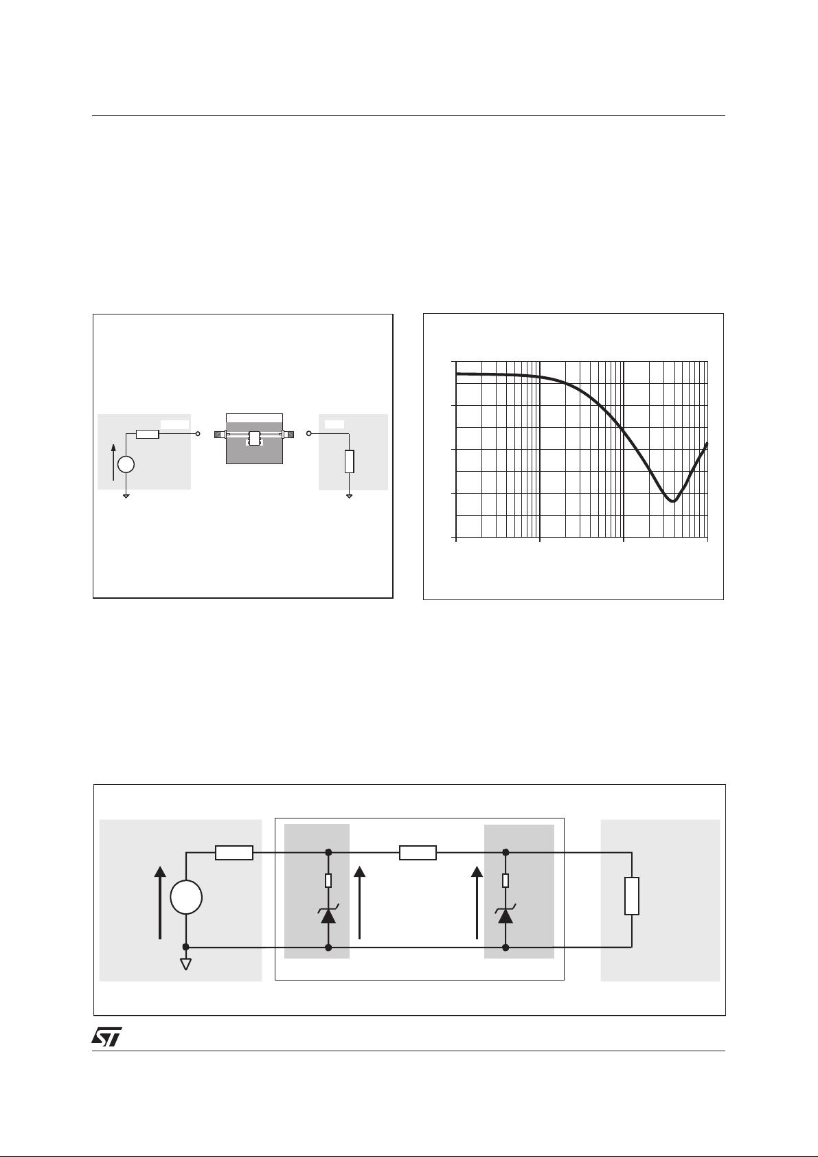
TECHNICAL INFORMATION
EMI FILTERING
TheKBMFxxSC6ensurea filtering protection against ElectroMagnetic and RadioFrequency Interferences
thanks to its low-pass filter structure. This filter is characterized by the following parameters :
- cut-off frequency
- Insertion loss
- high frequency rejection
Fig. A1: Measurements configuration
TG OUT
50 Ω
Vg
TEST BOARD
KM1
RF IN
50 Ω
Fig. A2: KBMFxxSC6 attenuation curve
Insertion loss (dB)
0
-10
-20
-30
-40
1 10 100 1000
F (MHz)
ESD PROTECTION
The KBMFxxSC6 is particularly optimized to perform ESD protection. ESD protection is based on the use
of device which clamps at :
Vouput V R I
BR d PP
=+.
This protection function is splitted in 2 stages. As shown in figure A3, the ESD strikes are clamped by the
first stage S1 and then its remaining overvoltage is applied to the second stage through the resistor R.
Such a configuration makes the output voltage very low at the Voutput level.
Fig. A3: ESD clamping behavior
Rg
V
PP
ESD Surge
V
Rd
BR
S1
Rs
Vinput
Voutput
KBMFxxSC6
S2
Rd
V
Rload
BR
Device
to be
protected
3/8
Page 4

KBMFxxSC6
To have a good approximation of the remaining voltages at both Vinput and Voutput stages, we give the
typical dynamical resistance value Rd. By taking into account these following hypothesis : Rt>Rd, Rg>Rd
and Rload>Rd, it gives these formulas:
Vinput
Voutput
RV RV
gBR dg
=
=
+..
R
g
SBR d
R V R Vinput
+..
R
t
The results of the calculation done for V
=8kV, Rg=330Ω (IEC 61000-4-2 standard), Vbr=7V
PP
(typ.) and Rd = 1ohm (typ.) give:
Vinput = 31.2 V
Voutput = 7.8 V
This confirms the very low remaining voltage across the device to be protected. It is also important to note
that in this approximation the parasitic inductance effect was not taken into account. This could be few
tenths of volts during few ns at the input side. This parasitic effect is not present at the output side due the
low current involved after the resistance R
.
S
The measurements done here after show very clearly (Fig. A5) the high efficiency of the ESD protection :
- no influence of the parasitic inductances on output stage
- Voutput clamping voltage very close to Vbr (positive strike) and -Vf (negative strike)
Fig. A4: Measurement conditions
ESD
SURGE
16kV
TEST BO ARD
KM1
Air
Discharge
Vin
Vout
4/8
Page 5

KBMFxxSC6
Fig. A5: Remaining voltage at both stages S1 (Vinput) and S2 (Voutput) during ESD surge.
a. Positive surge
b. Negative surge
Please note that the KBMFxxSC6 is not only acting for positiveESDsurgesbutalsofornegativeones.For
these kind of disturbances it clamps close to ground voltage as shown in Fig. A5b.
LATCH-UP PHENOMENA
The early ageing and destruction of IC’s is often due to latch-up phenomena which is mainly induced by
dV/dt. Thanks to its structure, the KBMFxxSC6 provides a high immunity to latch-up phenomena by
smoothing very fast edges.
CROSSTALK BEHAVIOR
Fig. A6: Crosstalk phenomena
R
G1
V
G1
R
G2
V
G2
Line 1
Line 2
R
L1
R
L2
αβ
αβ
V+ V
1G1 12G2
V+ V
2G2 21G1
DRIVERS
Thecrosstalkphenomena is duetothe coupling between2 lines. Thecouplingfactor ( β
RECEIVERS
orβ21)increases
12
when the gap across lines decreases, this is the reason why we provide crosstalk measurements for
monolithic device to guarantee negligeable crosstalk between the lines. In the example above the expected signal on load R
partofthe V
signalrepresentsthe effect ofthecrosstalk phenomenon oftheline 1 ontheline 2. Thisphe-
G1
is α2VG2, in fact the real voltage at this point has got an extra value β21VG1. This
L2
nomenon has to be taken into account when the drivers impose fast digital data or high frequency analog
signals in the disturbing line. The perturbed line will be more affected if it works with low voltage signal or
high load impedance (few kΩ).
5/8
Page 6

KBMFxxSC6
Fig. A7: Analog Crosstalk measurements configu-
ration
Fig. A8: Typical Analog Crosstalk measurement
crosstalk (dB)
0
-20
TG OUT
50 Ω
Vg
TEST BOARD
KM1
RF IN
50 Ω
-40
-60
-80
-100
-120
1 10 100 1,000
F (MHz)
Figure A7givesthemeasurementcircuitforthe analog crosstalk application. In figure A8, the curve shows
the effect of the Data line on the CLK line. In usual frequency range of analog signals (up to 100MHz) the
effect on disturbed line is less than -37dB.
Fig. A9: Digital crosstalk measurements configu-
Fig. A10: Digital crosstalk measurements
ration
+5V +5V
Square
Pulse
Generator
5KHz
+5V
74HC04
Line 1
V
G1
Line 2
KBMF
01SC6
74HC04
b
V
21
G1
Figure A9 shows the measurement circuit used to quantify the crosstalk effect in a classical digital application.
Figure A10 shows that in such a condition signal from 0 to 5V and rise time of few ns, the impact on the
otherlineisless than 50mV peak topeak.(Below the logic high thresholdvoltage).Themeasurementsperformed with falling edges gives the results within the same range.
6/8
Page 7

APPLICATION EXAMPLE
Fig. A11: Implementation of KBMFxxSC6 in a typical application
KBMFxxSC6
KDAT
KCLK
Vcc
KBMF
01SC6
PS/2 Connector
PS/2 Keyboard
Super I/O
MDAT
KBMF
MCLK
The KBMFxxSC6 device could be used on PS/2 mouse or keyboard as indicated by figure A11.
01SC6
PS/2 Mouse
7/8
Page 8

KBMFxxSC6
PACKAGE MECHANICAL DATA.
SOT23-6L
E
e
D
e
C
θ
L
H
b
A1
RECOMMENDED FOOTPRINT (mm)
0.60
0.024
A
A2
REF. DIMENSIONS
Millimeters Inches
Min. Typ. Max. Min. Typ. Max.
A 0.90 1.45 0.035 0.057
A1 0 0.10 0 0.004
A2 0.90 1.30 0.035 0.0512
b 0.35 0.50 0.0137 0.02
c 0.09 0.20 0.004 0.008
D 2.80 3.00 0.11 0.118
E 1.50 1.75 0.059 0.0689
e 0.95 0.0374
H 2.60 3.00 0.102 0.118
L 0.10 0.60 0.004 0.024
θ 10° 10°
MECHANICAL SPECIFICATIONS
Lead plating Tin-lead
1.20
0.047
25µm max
Lead material Sn / Pb
Lead plating thickness 5µm min
3.50
0.138
2.30
0.090
mm
inch
1.10
0.043
(70% to 90%Sn)
Lead coplanarity 10µm max
Body material Molded epoxy
0.95
0.037
Flammability UL94V-0
MARKING
Type Order Code Weight Marking Package Base Qty
KBMF01SC6 KBMF01SC6 16.7mg KM1 SOT23-6L 3000
Informationfurnished is believedto be accurateandreliable. However, STMicroelectronicsassumes no responsibilityforthe consequences of
useof such informationnor for anyinfringement of patentsor other rightsof third partieswhich may resultfromits use. Nolicense is grantedby
implication or otherwise under any patent or patent rights of STMicroelectronics. Specifications mentioned in this publication are subject to
change without notice. This publication supersedes and replaces all information previously supplied.
STMicroelectronics products are not authorized for use as critical components in life support devices or systems without express written approval of STMicroelectronics.
The ST logo is a registered trademark of STMicroelectronics
© 2002 STMicroelectronics - Printed in Italy - All rights reserved.
STMicroelectronics GROUP OF COMPANIES
Australia - Brazil - Canada - China - Finland - France - Germany
Hong Kong - India - Israel - Italy - Japan - Malaysia - Malta - Morocco - Singapore
Spain - Sweden - Switzerland - United Kingdom - United States.
8/8
http://www.st.com
 Loading...