

Page 1

KBD43W13
Keyboard and PS/2 Mouse Controller
FEATURES
• Supports IBM PC and Compatible System
Designs
• Full Hardwire Design Based on Advanced
VLSI CMOS Technology
• Supports PS/2 Mouse
• 6 MHz to 12 MHz Operating Frequency
• Supports AT Mode and PS/2 Mode for
Different Hardware Configurations
• Automatically Detects PS/2 Mode or AT
Mode
• Much Faster Than Traditional Keyboard
Controllers
• 40 Pin DIP or 44 Pin PLCC Package
GENERAL DESCRIPTION
The KBD43W13 is a keyboard controller
designed to provide the functions needed to
interface a CPU to a keyboard or to a PS/2
mouse. The KBD43W13 can be used with IBM®compatible personal computers or PS/2-based
systems. The controller receives serial data from
the keyboard or PS/2 mouse, checks the parity
of the data, and presents the data to the system
as a byte of data in its output buffer. The
controller will interrupt the system when data is
placed in its output buffer. The keyboard and
PS/2 mouse are required to acknowledge all
data transmissions. No transmission should be
sent to the keyboard or PS/2 mouse until
acknowledgment is received for the previous
byte sent.
This fast keyboard controller can improve the
performance of IBM PC machines and their
compatibles. A hardwired methodology is used in
this controller instead of a software
implementation, as in the traditional 8042
keyboard BIOS. With full hardware
implementation, this enables the keyboard
controller to respond instantly to all commands
sent from the keyboard and PS/2 mouse to the
CPU BIOS.
The keyboard controller enables popular
programs such as AutoCAD®, Microsoft
®
Windows™, NOVELL®, and other programs to
run much faster.
IBM is a registered trademark of International Business
Machines Corporation. AutoCAD is a registered trademark
of Autodesk, Inc. Microsoft is a registered trademark and
Windows is a trademark of Microsoft Corporation.
NOVELL is a registered trademark of Novell, Inc.
Standard Microsystems is a registered trademark and
SMSC is a trademark of Standard Microsystems
Corporation. Other product and company names are
trademarks or registered trademarks of their respective
holders.
Page 2

2
TABLE OF CONTENTS
FEATURES....................................................................................................................................... 1
GENERAL DESCRIPTION ................................................................................................................ 1
PIN CONFIGURATIONS.................................................................................................................... 3
PIN DESCRIPTION ........................................................................................................................... 4
BLOCK DIAGRAM............................................................................................................................ 6
ABSOLUTE MAXIMUM RATINGS..................................................................................................... 7
ELECTRICAL CHARACTERISTICS & CAPACITANCE..................................................................... 7
OUTPUT BUFFER............................................................................................................................. 8
INPUT BUFFER ................................................................................................................................ 8
(A) INPUT PORT DEFINITION (AT MODE) .............................................................................................. 9
(B) OUTPUT PORT DEFINITION (AT MODE)........................................................................................... 9
(C) TEST-INPUT PORT DEFINITION (AT MODE)...................................................................................... 9
STATUS REGISTER (PS/2 MODE)...................................................................................................... 10
INPUT PORT DEFINITION................................................................................................................... 10
OUTPUT PORT DEFINITION................................................................................................................ 11
TEST-INPUT PORT DEFINITION........................................................................................................... 11
COMMANDS (I/O ADDRESS HEX 64) (AT MODE)................................................................................ 11
COMMANDS (I/O ADDRESS HEX 64) (PS/2 MODE)............................................................................. 12
AC TIMING...................................................................................................................................... 14
TIMING WAVEFORMS.................................................................................................................... 15
WRITE CYCLE TIMING ...................................................................................................................... 15
READ CYCLE TIMING........................................................................................................................ 15
RECEIVE DATA FROM K/B................................................................................................................. 16
TYPICAL APPLICATION CIRCUITS................................................................................................ 18
APPLICATION FOR AT MODE............................................................................................................. 18
APPLICATION FOR PS/2 MODE.......................................................................................................... 19
DRIVING FROM EXTERNAL SOURCE.................................................................................................... 20
PACKAGE DIMENSIONS ................................................................................................................ 21
80 Arkay Drive
Hauppauge, NY 11788
(516) 435-6000
FAX (516) 273-3123
Page 3
3
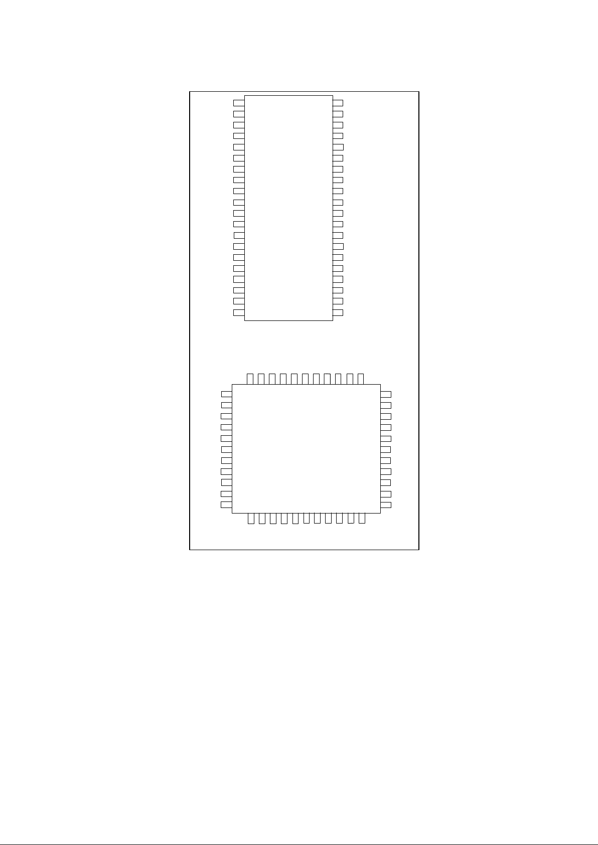
PIN CONFIGURATIONS
T0
X1
X2
nRESET
V
CC
CS
GND
nRD
A2
nWR
NC
D0
D1
D2
D3
D4
D5
D6
D7
GND
1
2
3
4
5
6
7
8
9
10
11
12
13
14
15
16
17
18
19
20
40
39
38
37
36
35
34
33
32
31
30
29
28
27
26
25
24
23
22
21
V
CC
T1
P27(KDAT)
P26(KCLK)
P25(IEMP/MINT)
P24(KINT)
P17(KINH)
P16(DISP)
P15(JUMP)
P14(RAM)
P13
P12
P11
P10
NC
V
CC
P23(NC/MCLK)
P22(NC/MDAT)
P21(nGA20)
P20(nRC)
40 Pin DIP
7
8
9
10
11
12
13
14
15
16
17
nCS
GND
nRD
A2
nWR
NC
NC
D0
D1
D2
D3
1819202122232425262728
D4D5D6
D7
GND
NC
P20
P21
P22
P23
V
CC
39
38
37
36
35
34
33
32
31
30
29
P24
P17
P16
P15
P14
NC
P13
P12
P11
P10
NC
65432
1
4443424140
VCCnRESETX2X1T0NC
VCCT1
P27
P26
P25
44 Pin PLCC
Page 4

4
PIN DESCRIPTION
PIN NO. FUNCTION
(40 Pin
DIP)
(44 Pin
PLCC) I/O NAME AT MODE PS/2 MODE
1 2 I T0 K/B Clock Input K/B Clock Input
2 3 I X1 Crystal Clock I/P Crystal Clock I/P
3 4 I X2 Crystal Clock I/P Crystal Clock I/P
4 5 I nRESET Chip Reset Chip Reset
5 6 - VCC Optional +5V Power
Supply
Optional + 5V Power
Supply
6 7 I nCS Chip Select Chip Select
7 8 - GND Optional Ground
Power
Optional Ground
Power
8 9 I nRD I/O Read I/O Read
9 10 I A2 Connect to AddressA2Connect to Address
A2
10 11 I nWR I/O Write I/O Write
11,26 1,12,13,
23,29,34
- NC Reserved Reserved
12,13,14,
15,16,17,
18,19
14,15,16,
17,18,19,
20,21
I/O
D0−D7 Data Bus D0−D7 Data Bus D0−D7
20 22 - GND Ground Power
Supply
Ground Power Supply
21 24 O P20 Bit 0 of Port2
(nRC: System
Reset)
Bit 0 of Port2
(
nRC
: System Reset)
22 25 O P21 Bit 1 of Port2
(
nGA20
: GATE A20)
Bit 1 of Port2
(
nGA20
: GATE A20)
23 26 I/O P22 Bit 2 of Port2
(NC: User-defined
I/O)
Bit 2 of Port2
(MDAT: Mouse Data
Output)
24 27 I/O P23 Bit 3 of Port2
(NC: User-defined
I/O)
Bit 3 of Port2
(MCLK: Mouse Clock
Output)
25 28 - VCC Optional +5V Power
Supply
Optional + 5V Power
Supply
27 30 I/OPU* P10 Bit 0 of Port1
(User-defined I/O)
Bit 0 of Port1
(K/B Data Input)
28 31 I/OPU* P11 Bit 1 of Port1
(User-defined I/O)
Bit 1 of Port1
(Mouse Data Input)
29 32 I/O P12 Bit 2 of Port2
(User-defined I/O)
Bit 2 of Port2
(User-defined I/O)
30 33 I/O P13 Bit 3 of Port1
(User-defined I/O)
Bit 3 of Port1
(User-defined I/O)
Page 5

5
PIN NO. FUNCTION
(40 Pin
DIP)
(44 Pin
PLCC) I/O NAME AT MODE PS/2 MODE
31 35 I PU* P14 Bit 4 of Port1
(RAM: RAM Jumper
Select)
Bit 4 of Port1
(RAM: RAM Jumper
Select)
32 36 I PU* P15 Bit 5 of Port1
(JUMP: Jumper)
Bit 5 of Port1
(JUMP: Jumper)
33 37 I PU* P16 Bit 6 of Port1
(DISP: Display
Select)
Bit 6 of Port1
(DISP: Display
Select)
34 38 I
PU*
P17 Bit 7 of Port1
(KINH: K/B Inhibit
Switch)
Bit 7 of Port1
(KINH: K/B Inhibit
Switch)
35 39 O P24 Bit 4 of Port2
(KINT: K/B OBF O/P
Interrupt)
Bit 4 of Port2
(KINT: K/B OBF O/P
Interrupt)
36 40 O P25 Bit 5 of Port2
(IEMP: I/P Buffer
Empty)
Bit 5 of Port2
(MINT: Mouse OBF
O/P Interrupt)
37 41 O P26 Bit 6 of Port2
(KCLK: K/B Clock
Output)
Bit 6 of Port2
(KCLK: K/B Clock
Output)
38 42 O P27 Bit 7 of Port2
(KDAT: K/B Data
Output)
Bit 7 of Port2
(KDAT: K/B Data
Output)
39 43 I T1 K/B Data Input Mouse Clock Input
40 44 - Vcc +5V Power Supply +5V Power Supply
* Internal pull-up resistor
Page 6
6
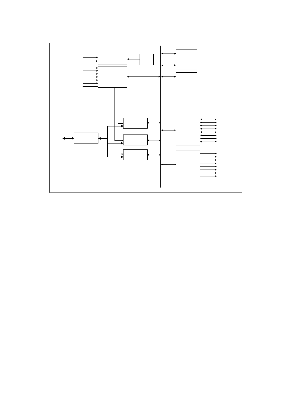
BLOCK DIAGRAM
SCAN
CODE
ROM
RECEIVE
CONTROL
HARDWIRE
CONTROL &
SELECT
LOGIC
STATUS
BUFFER
REGISTER
R64
W60
W64
R60
INPUT
BUFFER
REGISTER
BUFFER
REGISTER
OUTPUT
DATA
BUFFER
REGISTER
D0~D7
T0
T1
nWR
nRD
nCS
A2
nRESET
TRANSMIT
CONTRROL
REGISTER
STATUS
TRANSMIT
REGISTER
INPUT &
OUTPUT
PORT
INTERFACE
OUTPUT
PORT
INTERFACE
P20 (nRC)
P21 (nGA20)
P22 (NC/MDAT)
P23 (NC/MCLK)
P24 (KINT)
P25 (IEMP/MINT)
P26 (KCLK)
P27 (KDAT)
P10
P11
P12
P13
P14 (RAM)
P15 (JUMP)
P16 (DISP)
P17 (KINH)
x2
x1
Page 7
7
ABSOLUTE MAXIMUM RATINGS
PARAMETER RATING UNIT
Ambient Operating Temperature -0 to + 85
°C
Storage Temperature -65 to + 150
°C
Supply Voltage to Ground Potential -0.3 to + 7.0 V
Applied Input/Output Voltage -0.3 to + 7.0 V
Power Dissipation 50 mW
Note: Exposure to conditions beyond those listed under Absolute Maximum Ratings may adversely
affect the life and reliability of the device.
ELECTRICAL CHARACTERISTICS & CAPACITANCE
(Ta = 0° C to + 70° C, VDD = +5V ± 5%)
SYMBOL DESCRIPTION MIN. TYP. MAX. UNIT NOTE
VDD Power Supply 4.75 5.0 5.25 V
VIL Input Low Voltage (except
RESET, T0, T1)
0.8 V
VIL1 Input Low Voltage (RESET,
T0,T1)
0.6 V
VIH1 Input High Voltage (except
RESET, T0, T1, P10, P11)
2.0 V
VIH2 Input High Voltage (P10,P11) 3.0 V
VIH3 Input High Voltage (T0,T1,
RESET)
3.5 V
VOH1 Output High Voltage
(P10−P13, P20−P27)
2.4 V IOH = -2 mA
VOH2
Output High Voltage (D0−D7)
2.4 V IOH = -4 mA
VOL1
Output Low Voltage (P10−P13,
P20−P27)
0.4 V IOL = 2 mA
VOL2
Output Low Voltage (D0−D7)
0.4 V IOL = 4 mA
RIP Min. I/P Resist 10K
Ω
IOFL
O/P Leakage Current (D0−D7,
High Z State)
-10 10
µA
IIH I/P Leakage Current -10 10
µA
VDD = 5.5V,
VIN = VDD
IIL I/P Leakage Current (Except
P10, P11, P14, P15, P16, P17)
-10 10
µA
VDD = 5.5V,
VIN = VSS
IIL1 I/P Leakage Current (P10,
P11, P14, P15, P16, P17)
-10 550
µA
VDD = 5.5V,
VIN = VSS
CL O/P Load Capacity 15 50 pF
Page 8

8
STATUS REGISTER (AT MODE)
The status register is an 8-bit read-only register at I/O address hex 64 that holds information about the
status of the keyboard controller and interface. It may be read at any time.
BIT BIT FUNCTION DESCRIPTION
0 Output Buffer Full 0: Output buffer empty
1: Output buffer full
1 Input Buffer Full 0: Input buffer empty
1: Input buffer full
2 System Flag This bit may be set to 0 or 1 by writing to the system flag bit in
the command byte of the keyboard controller. It is set to 0 after
a power-on reset
3 Command/data 0: Data byte
1: Command byte
4 Inhibit Switch 0: Keyboard is inhibited
1: Keyboard is not inhibited
5 Transmit Time-out 0: No transmit time-out error
1: Transmit time-out error
6 Receive Time-out 0: No receive time-out error
1: Receive time-out error
7 Parity Error 0: Odd parity (no error)
1: Even parity (error)
OUTPUT BUFFER
The output buffer is an 8-bit read-only register at I/O address hex 60. The keyboard controller uses the
output buffer to send the scan code received from the keyboard and data bytes required by commands
to the system. The output buffer should be read only when the output buffer full bit in the register is 1.
INPUT BUFFER
The input buffer is an 8-bit write-only register at I/O address hex 60 or 64. Writing to address hex 60
sets a flag that indicates a data write; writing to address hex 64 sets a flag that indicates a command
write. Data written to I/O address hex 60 are sent to the keyboard (unless the keyboard controller is
expecting a data byte) following the controller's input buffer only if the input buffer full bit in the status
register is set to 0.
Page 9

9
(A) Input Port Definition (AT Mode)
BIT FUNCTION
0 Undefined
1 Undefined
2 Undefined
3 Undefined
4 RAM on System Board
0: Disable second 256 KB of system board RAM
1: Enable second 256 KB of system board RAM
5 Manufacturing Jumper Installed
0: Manufacturing jumper
1: Jumper not installed
6 Display Type Switch
0: Primary display attached to color/graphics
1: Primary display attached to monochrome
7 Keyboard Inhibit Switch
0: Keyboard inhibited
1: Keyboard not inhibited
(B) Output Port Definition (AT Mode)
BIT FUNCTION
0 System Reset
1 Gate A20
2 Undefined
3 Undefined
4 Output Buffer Full
5 Input Buffer Empty
6 Keyboard Clock (Output)
7 Keyboard Data (Output)
(C) Test-input Port Definition (AT Mode)
BIT FUNCTION
0 Keyboard Clock (Input)
1 Keyboard Data (Input)
Page 10

10
Status Register (PS/2 Mode)
BIT BIT FUNCTION DESCRIPTION
0 Output Buffer Full 0: Output buffer empty
1: Output buffer full
1 Input Buffer Full 0: Input buffer empty
1: Input buffer full
2 System Flag This bit may be set to 0 or 1 by writting to the
system flag bit in the command byte of the keyboard
controller. It is set to 0 after a power-on reset.
3 Command/Data 0: Data byte
1: Command byte
4 Inhinit Switch 0: Keyboard is inhibited
1: Keyboard is not inhibited
5 Auxiliary Device Output Buffer 0: Auxiliary device output buffer empty
1: Auxiliary device output buffer full
6 General Purpose Time-out 0: No time-out error
1: Time-out error
7 Parity Error 0: Odd parity
1: Even parity (error)
Input Port Definition
BIT FUNCTION
0 Keyboard Data Input
1 Mouse Data Input
2 Undefined
3 Undefined
4 RAM on System Board
0: Disable second 256 KB of system board RAM
1: Enable second 256 KB of system board RAM
5 Manufacturing Jumper
0: Manufacturing jumper
1: Jumper not installed
6 Display Type Switch
0: Primary display attached to color/graphics
1: Primary display attached to monochrome
7 Keyboard Input Switch
0: Keyboard inhibited
1: Keyboard not inhibited
Page 11

11
Output Port Definition
BIT FUNCTION
0 System Reset
1 Gate A20
2 Mouse Data Output
3 Mouse Clock Output
4 Keyboard Output Buffer Full Interrupt
5 Mouse Output Buffer Full Interrupt
6 Keyboard Clock Output
7 Keyboard Data Output
Test-input Port Definition
BIT FUNCTION
0 Keyboard Clock Input
1 Mouse Clock Input
Commands (I/O Address HEX 64) (AT Mode)
COMMAND FUNCTION
20 Read Command Byte of Keyboard Controller
60 Write Command Byte of Keyboard Controller
BIT
1
2
3
4
5
6
7
0
BIT DEFINITION
Reserved
IBM PC Compatible Mode
IBM PC Mode
Disable Keyboard
Inhibit Override
System Flag
Reserved
Enable Output Buffer Full Interrupt
AA Self-test
AB Interface Test
BIT
04
03
02
01
00
BIT DEFINITION
No Error Detected
K/B Clock Line is Stuck Low
K/B Clock Line is Stuck High
K/B Data Line is Stuck Low
K/B Data Line is Stuck High
AD Disable Keyboard Feature
Page 12

12
COMMAND FUNCTION
AE Enable Keyboard Interface
C0 Read Input Port
D0 Read Output Port
D1 Write Output Port
E0 Read Test Inputs
F0-FF Pulse Output Port
Commands (I/O Address HEX 64) (PS/2 Mode)
COMMAND FUNCTION
20 Read Command Byte of Keyboard Controller
60 Write Command Byte of Keyboard Controller
BIT
1
2
3
4
5
6
7
0
BIT DEFINITION
Reserved
IBM Keyboard Translate Mode
Disable Auxiliary Device
Disable Keyboard
Reserve
System Flag
Enable Auxiliary Interrupt
Enable Keyboard Interrupt
A7 Disable Auxiliary Device Interface
A8 Enable Auxiliary Device Interface
A9 Interface Test
BIT
04
03
02
01
00
BIT DEFINITION
No Error Detected
Auxiliary Device "Clock" line is stuck low
Auxiliary Device "Clock" line is stuck high
Auxiliary Device "Data" line is stuck low
Auxiliary Device "Data" line is stuck low
AA Self-test
Page 13

13
COMMAND FUNCTION
AB Interface Test
BIT
04
03
02
01
00
BIT DEFINITION
No Error Detected
Keyboard "Clock" line is stuck low
Keyboard "Clock" line is stuck high
Keyboard "Data" line is stuck low
Keyboard "Data" line is stuck high
AD Disable Keyboard Interface
AE Enable Keyboard Interface
C0 Read Input Port
C1 Poll Input Port Low
C2 Poll Input Port High
D0 Read Output Port
D1 Write Output Port
D2 Write Keyboard Output Buffer
D3 Write Auxiliary Device Output Buffer
D4 Write to Auxiliary Device
E0 Read Test Inputs
F0-FF Pulse Output Port
Page 14

14
AC TIMING
NO. DESCRIPTION MIN. MAX. UNIT
T1 Address Setup Time from WRB 0 nS
T2 Address Setup Time from RDB 0 nS
T3 WRB Strobe Width 20 nS
T4 RDB Strobe Width 20 nS
T5 Address Hold Time from WRB 0 nS
T6 Address Hold Time from RDB 0 nS
T7 Data Setup Time 50 nS
T8 Data Hold Time 0 nS
T9 Gate Delay Time from WRB 10 30 nS
T10 RDB to Drive Data Delay 40 nS
T11 RDB to Floating Data Delay 0 20 nS
T12 Data Valid After Clock Falling (SEND) 4
µS
T13 K/B Clock Period 20
µS
T14 K/B Clock Pulse Width 10
µS
T15 Data Valid Before Clock Falling (RECEIVE) 4
µS
T16 K/B ACK After Finish Receiving 20
µS
T17 RC Fast Reset Pulse Delay (8 MHz) 2 3
µS
T18 RC Pulse Width (8 MHz) 6
µS
T19 Transmit Timeout 2 mS
T20 Data Valid Hold Time 0
µS
T21
X1/X2 Period (6−12 MHz)
83 167 nS
T22 Duration of CLK inactive 30 50
µS
T23 Duration of CLK active 30 50
µS
T24 Time from inactive CLK transition, used to time when
the auxiliary device sample DATA
5 25
µS
T25 Time of inhibit mode 100 300
µS
T26 Time from rising edge of CLK to DATA transition 5 T28-5
µS
T27 Duration of CLK inactive 30 50
µS
T28 Duration of CLK active 30 50
µS
T29 Time from DATA transition to falling edge of CLK 5 25
µS
T30 Mode detect signal after P10 goes high Typical 1 mS
T31 High pulse of mode detect signal
Typical 220 µS
T32 Low pulse of mode detect signal
Typical 220 µS
T33 Mode detect signal after RESET goes high Typical 1 mS
T34 Time out of AT mode‘ s mode detect signal Typical 64 mS
Page 15

15
TIMING WAVEFORMS
Write Cycle Timing
T1
T3
T7
T8
T9
T17
T18
ACTIVE
DATA IN
A2, CSB
WRB
D0~D7
GA20
OUTPUT PORT
FAST RESET PULSE RC
FE COMMAND
T5
Read Cycle Timing
DATA OUT
ACTIVE
T2
T4
T6
T10 T11
A2,CSB
AEN
RDB
D0-D7
Send Data to K/B
CLOCK
(KCLK)
SERIAL DATA
(KDAT)
D0
D1
D2 D3 D4
D5
D6 D7 P
STOP
START
T12
T14
T13 T16
T19
Page 16

16
Receive Data from K/B
CLOCK
(KCLK)
SERIAL DATA
(T1)
T15
T14 T13
T20
D0
D1 D2 D3 D4
D5
D6 D7 P
STOP
START
X1/X2 Clock
T21
CLOCK
CLOCK
Send Data to Mouse
MCLK
MDAT
T25
T22
T23
T24
D0
D1
D2 D3 D4
D5
D6 D7 P
STOP
Bit
START
Bit
Receive Data from Mouse
T29
T26 T27
MCLK
T28
MDAT
D0
D1 D2 D3 D4
D5
D6 D7 P
STOP
Bit
START
Page 17

17
PS2 Mode's Mode Detect
(P10 released to high by keyboard before RESET goes high)
RESET
P27
P10
T31
T32
T33
PS2 Mode's Mode Detect
(P10 released to high by keyboard after RESET goes high)
RESET
P27
P10
T31
T32
T30
AT Mode's Mode Detect
(P10 internal pull high. As there is no external loop between P27 and P10 so P27 issues pulse until time
out)
RESET
P27
P10
T31
T33
T32
T34
Page 18

18
TYPICAL APPLICATION CIRCUITS
Application for AT Mode
X1
2
X2
3
RESET
4
T0
1
T1
39
A2
9
nCS
6
Vcc
5
nRD
8
nWR
10
D0
12
D1
13
D2
14
D3
15
D4
16
D5
17
D6
18
D7
19
GND
7
GND
20
Vcc
40
Vcc
25
P10
27
P11
28
P12
29
P13
30
P14
31
P15
32
P16
33
P17
34
P20
21
P21
22
P22
23
P23
24
P24/OB
35
P25
36
P26/KCLK
37
P27/KDAT
38
NC
11
NC
26
KB8042-DIP
RAM SELECT JUMPER
MANUFACTURING MODE JUMPER
RCB
GATE20
RESETB
SA2
n8042CS
nIORD
nIOWR
D[0..7]
1 2
74ALS04
KEYBOARD INTERRUPT
Vcc
1 2
7407
KEYBOARD CLOCK
KEYBOARD DATA
1 2
7407
Page 19

19
Application for PS/2 Mode
KEYBOARD INTERRUPT
X1
2
X2
3
RESET
4
T0
1
T1
39
A2
9
nCS
6
Vcc
5
nRD
8
nWR
10
D0
12
D1
13
D2
14
D3
15
D4
16
D5
17
D6
18
D7
19
GND
7
GND
20
Vcc
40
Vcc
25
P10
27
P11
28
P12
29
P13
30
P14
31
P15
32
P16
33
P17
34
P20
21
P21
22
P22
23
P23
24
P24/OB
35
P25
36
P26/KCLK
37
P27/KDAT
38
NC
11
NC
26
KB8042-DIP
PS/2 MOUSE INTERRUPT
RAM SELECT JUMPER
MANUFACTURING MODE JUMPER
RCB
GATE20
RESETB
SA2
n8042CS
nIORD
nIOWR
D[0..7]
1 2
7406
Vcc
PS/2 MOUSE DATA
Vcc
PS/2 MOUSE CLOCK
1 2
7406
1 2
7406
1 2
7406
KEYBOARD CLOCK
KEYBOARD DATA
Page 20

20
Driving from External Source
OPTION 2
PCLK
X1
1 2
2
X2
3
N.C.
OPTION 1
2
X1
3
X2
1 2
PCLK
OPTION 3
+5V
470 470
PCLK
1 2
7404
1 2
7407
2
X1
X2
3
1 2
7407
Page 21

21
PACKAGE DIMENSIONS
40 Pin DIP
44 Pin PLCC
44 40
39
29
2818
17
7
6 1
L
c
1
b
2
A
H
D
D
e
b
E H
E
y
A
A
1
Seating Plane
D
G
G
E
Notes:
Symbol
Min. Nom. Max. Max.Nom.Min.
Dimension in inch
Dimension in mm
A
b
c
D
e
H
E
L
y
A
A
1
2
E
b
1
H
D
G
G
D
E
on final visual inspection spec.
4. General appearance spec. should be based
3. Controlling dimension: Inches
protrusion/intrusion
2. Dimension b1 does not include dambar
flash.
1. Dimensions D & E do not include interlead
0.020
0.145
0.026
0.016
0.008
0.648
0.590
0.680
0.090
0.150
0.028
0.018
0.010
0.653
0.610
0.690
0.100
0.050
BSC
0.185
0.155
0.032
0.022
0.014
0.658
0.630
0.700
0.110
0.004
0.51
3.68
0.66
0.41
0.20
16.46
14.99
17.27
2.29
3.81
0.71
0.46
0.25
16.59
15.49
17.53
2.54
1.27
4.70
3.94
0.81
0.56
0.36
16.71
16.00
17.78
2.79
0.10
BSC
16.71
16.59
16.46
0.658
0.653
0.648
16.00
15.4914.99
0.6300.610
0.590
17.7817.5317.27
0.7000.690
0.680
1. Dimensions D Max & S include mold flash or
tie bar burrs.
2. Dimension E1 does not include interlead flash.
3. Dimensions D & E1 include mold mismatch and
are determined at the mold parting line.
6. General appearance spec. should be based on
final visual inspection spec.
.
1.371.220.0540.048
Notes:
Symbol
Min.
Nom.
Max. Max.
Nom.
Min.
Dimension in inch
Dimension in mm
A
B
c
D
e
A
L
S
A
A
1
2
E
0.050 1.27
0.210
5.33
0.010
0.150
0.016
0.155
0.018
0.160
0.022
3.81
0.41
0.25
3.94
0.46
4.06
0.56
0.008
0.120
0.670
0.010
0.130
0.014
0.140
0.20
3.05
0.25
3.30
0.36
3.56
0.540
0.5500.545
13.72
13.9713.84
17.02
15.2414.99
15.49
0.6000.590 0.610
2.29 2.54 2.790.090 0.100
0.110
B
1
1
e
E
1
a
2.055 2.070
52.20
52.58
0 15
0.090 2.29
0.650
0.630 16.00
16.51
protrusion/intrusion.
4. Dimension B1 does not include dambar
5. Controlling dimension: Inches.
150
Seating Plane
e
A
2
A
a
c
E
Base Plane
1
A
1
e
L
A
S
1
E
D
1
B
B
40
21
20
1
Page 22

© 1998 STANDARD MICROSYSTEMS CORPORATION (SMSC)
Circuit diagrams utilizing SMSC products are included as a means of illustrating typical applications; consequently complete
information sufficient for construction purposes is not necessarily given. The information has been carefully checked and is believed
to be entirely reliable. However, no responsibility is assumed for inaccuracies. Furthermore, such information does not convey to the
purchaser of the semiconductor devices described any licenses under the patent rights of SMSC or others. SMSC reserves the right
to make changes at any time in order to improve design and supply the best product possible. SMSC products are not designed,
intended, authorized or warranted for use in any life support or other application where product failure could cause or contribute to
personal injury or severe property damage. Any and all such uses without prior written approval of an Officer of SMSC and further
testing and/or modification will be fully at the risk of the customer.
KBD43W13 Rev. 10/21/98
 Loading...