

Page 1

KB9224 VIDEO-CD 2ND GENERATION
KB9224
PRELIMINARY
DATA SHEET
1999.6.7
1
Page 2

VIDEO-CD 2ND GENERATION KB9224
INTRODUCTION
The KB9224 is a Servo Signal Processor designed specifically for the Samsung Video-CD designed using the
BICMOS process. RF Block and Picture Quality Enhancing Items are built-in. The processor is a Hard-wired FreeAdjustment Servo with the Pre-signal parts adjustment point automatically adjusted.
FEATURES
• Focus Error Amplifier & Servo Control
• Tracking Error Amplifier & Servo Control
• Sled Amplifier
• Embedded CLV Control LPF
• APC (Auto Laser Power Control) Circuit for Constant Laser Power
• Double Speed Play Available
• Circuit for Interruption Countermeasure
• Mirror, FOK & Defect Detector Circuit
• FE Bias & Focus Servo Offset Free Adjustment
• EF Balance & Tracking Loop Gain Free Adjustment
• Tracking Servo Offset Free Adjustment
• Enhanced Auto-Sequence Algorithm (Fast-Search)
• Tracking Mutting by Window Mirror
• Current, Voltage Pick-up Interaction available
• Embedded RF 3T Boost Circuit
• Enhanced RF Equalize AGC Circuit
• Built-in Envelope EFM Slicer
• Built-in DSP C1-flag Control Circuit
• RF Peaking Prevention Circuit
• Focus & Tracking mutting by EFM Duty Countermeasure
• Built-in Focus, Tracking 2x Filter Adjust
• Single Power Supply: +5 V
•- Related Products
. KS9287 Data Processor
. KA9258D/KA9259D Motor Driver
2
Page 3
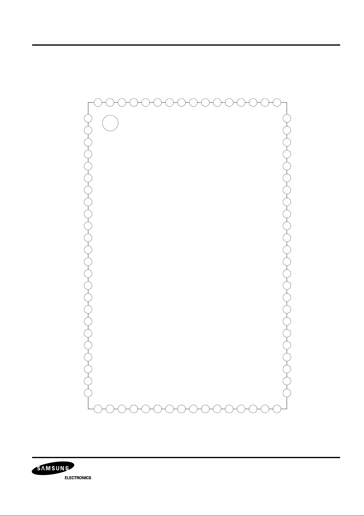
VIDEO-CD 2ND GENERATION KB9224
MIRROR
RESET
MDATA
TRCNT
PIN CONFIGURATION
PDA
PDC
PDB
PDD
F
E
PD
LD
VR
VCC
IVSEL
BOOSTC2
RFL
RF-
RFO
IRF
80
79
78
77
76
75
74
73
72
71
70
69
68
67
66
65
EQI
EQI2
RFI
ARF2
MOC
CAGC
GND
MCP
DCB
FRSH
DCC2
DCC1
FSET
VDDA
ENBR
10
11
12
13
14
15
DVEE
641
FEBIAS
2
3
4
5
6
7
8
9
KB9224
63
62
61
60
59
58
57
56
55
54
53
52
51
50
TG2
TGU
FDFCT
FE1
FE2
TDFCT
DVDD
LPFT
TE1
TE2
TZC
ATSC
TEO
ENC
ENVO
ISET
VREG
WDCK
SMDP
SMON
SMEF
DEFECT
16
17
18
19
20
21
22
23
24
25
FLB
26
FS3
27
FGD
28
LOCK
29
30
ISTAT
31
EFM
32
EFM2
33
ASY
34
VSSA
35
MCK
36
37
MLT
38
39
40
FOK
49
48
47
46
45
44
43
42
41
TE-
FEO
FE-
SPDLO
SPDL-
SL-
SLO
SL+
SSTOP
3
Page 4

VIDEO-CD 2ND GENERATION KB9224
PIN DESCRIPTION
No. Pin Name I/O Description
1 EQI I RF AGC & Eqaualize input pin
2 EQI2 I RF AGC & Equalize input connect switch (controled by Flag)
3 RFI I EFM COMPARATOR input pin
4 ARF O RF AGC & EQ output pin.
5 ARF2 O RF AGC & EQ output connect pin (controled by Falg)
6 CAGC I AGC_EQUALIZE LEVEL control pin, VCA input pin & NOISE eliminating CAP pin
7 GND G Ground (RF block)
8 MCP I Half-wave rectifier CAP pin for MIRROR output
9 DCB I DEFECT MAX DUTY limiting CAP pin
10 FRSH I FOCUS SEARCH generating & charge/discharge CAP pin
11 DCC1 O DEFECT MIN DUTY generating DC eliminating CAP pin. (connected DCC1)
12 DCC2 I DEFECT MIN DUTY generating DC eliminating CAP pin (connected DCC2)
13 FSET I FCOUS,TRACKING,SPINDLE PEAKING frequency compensation BIAS pin
14 VDDA P 5V POWER pin for SERVO
15 ENBR I BIAS pin for ENVELOPE EFM-SLICE
16 ENC I RF ENVELOPE DC BIAS extract voltage input pin
17 ENVO O RF ENVELOPE output pin
18 ISET I FOCUS SERARCH,TRACKING JUMP, SLED KICK voltage generating BIAS pin
19 VREG O 3.4 V REGULATOR output pin
20 WDCK I 88.2KHz input pin from DSP
21 SMDP I SMDP input pin of DSP
22 SMON I SMON input pin of DSP
23 SMEF I External LPF time constant connection pin of CLV servo error signal
24 DEFECT O DEFECT output pin.
25 FLB I CAP pin for FOCUS LOOP rising low band
26 FS3 I FOCUS LOOP’s high frequency gain adjustment pin
27 FGD I FOCUS LOOP’s high frequency gain adjustment pin
28 LOCK I SLED RUN AWAY preventing pin (L: Sled Off and Tracking Gain Up)
29 TRCNT O Track Count output pin
30 ISTAT O INTERNAL STATUS output pin
31 EFM O RFO SLICE EFM output pin (to DSP)
4
Page 5

VIDEO-CD 2ND GENERATION KB9224
PIN DESCRIPTION (Continued)
No. Pin Name I/O Description
32 EFM2 O EFM comparator integrating output pin
33 ASY I AUTO asymmetry control input pin
34 VSSA G SERVO part analog VSSA power supply PIN
35 MCK I MICOM clock pin
36 MDATA I DATA input pin
37 MLT I DATA LATCH input pin
38 RESET I RESET input pin
39 MIRROR O MIRROR detect output pin
40 FOK O FOCUS OK output pin
41 SSTOP I PICK UP's maximum lead-in diameter position check pin
42 SL+ I SLED SERVO non-inverting input
43 SLO O SLED SERVO output
44 SL- I SLED SERVO inverting input
45 SPDL- I SPINDLE AMP inverting input pin
46 SPDLO O SPINDLE AMP output pin
47 FE- I FOCUS SERVO AMP inverting input pin
48 FEO O FOCUS SERVO AMP output pin
49 TE- I TRACKING SERVO AMP inverting input pin
50 TEO O TRACKING SERVO AMP output pin
51 ATSC I ANTI-SHOCK input pin
52 TZC I TRACKING ZERO CROSSING input pin
53 TE2 I TRACKING SERVO input pin
54 TE1 O TRACKING ERROR AMP output pin
55 LPFT I TRACKING ERROR integrating input pin (Auto adjust)
56 DVDD P LOGIC DVDD power supply pin
57 TDFCT I DEFECT TRACKING ERROR integrating CAP connection pin
58 FE2 I FOCUS SERVO input pin
59 FE1 O FOCUS ERROR AMP output pin
60 FDFCT I When DEFECT, FOCUS ERROR integrating CAP connection pin
61 TGU I High frequency TRACKING GAIN SWITCHING CAP connection pin
62 TG2 I Time constant controlling TRACKING LOOP's high frequency gain control pin
63 FEBIAS I FOCUS ERROR BIAS control connect pin
5
Page 6

VIDEO-CD 2ND GENERATION KB9224
PIN DESCRIPTION (Continued)
No. Pin Name I/O Description
64 DVEE G LOGIC DVEE power supply pin
65 PDA I POTO-DIODE A & RF I/V AMP1 inverting input pin
66 PDC I POTO-DIODE C & RF I/V AMP1 inverting input pin
67 PDB I POTO-DIODE B & RF I/V AMP2 inverting input pin
68 PDD I POTO-DIODE D & RF I/V AMP2 inverting input pin
69 F I POTO-DIODE F & TRACKING (F) I/V AMP inverting input pin
70 E I POTO-DIODE F & TRACKING (E) I/V AMP inverting input pin
71 PD I APC AMP input pin
72 LD O APC AMP output pin
73 VR O (VCC+GND)/2 VOLTAGE REFERENCE output pin
74 VCC P RF PART VCC power supply pin
75 IVSEL I Pick-UP Type Select pin(Default Pull Down)
76 BOOSTC2 I RF SUMMING AMP 3T BOOST's CAP connection pin (connected GND)
77 RFL I RF SUMMING AMP NOISE eliminating CAP connection pin (connected RFO)
78 RF- I RF SUMMING AMP inverting input pin
79 RFO O RF SUMMING AMP output pin
80 IRF I RFO DC eliminating input pin (Used in MIRROR, FOK pin)
6
Page 7
VIDEO-CD 2ND GENERATION KB9224
MICOM COMMAND
($0X, $1X)
Item
Focus Control 0 0 0 0
Tracking Control 0 0 0 1 Anti-
Tracking Gain Setting for Anti-Shock
D7 D6 D5 D4
0 0 0 1
Item Hex AS=0 AS=1
Tracking Gain Control
TG1, TG2=1 GAIN UP
AntiShock
Off
Address Data
Symbol D3 D2 D1 D0
FS4
Focus On
Shock
D3 D2 D1 D0
Anti-Shock Lens. Brake TG2 (D3=1) TG1
0 1 0 1 0 1 0 1
AntiShock
On
$10 0 0 0 0
$11 0 1 0 1
Lens
Brake
Off
TG2 TG1 TG2 TG1
Lens
Brake
On
FS3
Gain Down
Brake On TG2
High
Freq.
Gain
FS2
Search On
Gain Set
High
Freq.
Gain
Normal
Gain
FS1
Search Up
TG1
Gain Set
Gain
Up
ISTAT
Output
FZC
ATSC
ISTAT
Output
ATSC
$13,$17,$1B,$1F (AS0)
$13,$17,$18,$1C (AS1)
TRACKING GAIN UP
At this time, MIRROR
MUTTING is OFF
$12 1 0 1 0
$13 1 1 1 1
$14 0 0 0 0
$15 0 1 0 1
$16 1 0 1 0
$17 1 1 1 1
$18 0 0 1 1
$19 0 1 1 0
$1A 1 0 0 1
$1B 1 1 0 0
$1C 0 0 1 1
$1D 0 1 1 0
$1E 1 0 0 1
$1F 1 1 0 0
7
Page 8

VIDEO-CD 2ND GENERATION KB9224
$2X
D7 D6 D5 D4
D3 D2 D1 D0
Tracking Servo Mode Sled Servo Mode
0 0 1 0 Mode TM7 TM6 TM5 TM4 TM3 TM2 TM1
TM1 $20 1 0 1 0 1 1 0
0 Track. Servo Off $21 1 0 1 0 1 0 0
1 Track. Servo On $22 1 0 0 0 1 1 0
TM2 $23 1 1 1 0 1 1 0
0 Sled. Servo Off $24 1 0 1 0 1 1 1
1 Sled. Servo On $25 1 0 1 0 1 0 1
TM4 TM3 Track. Kick $26 1 0 0 0 1 1 1
0 0 FWD. Jump $27 1 1 1 0 1 1 1
0 0 Jump Off $28 1 0 1 0 0 1 0
0 0 REV. Jump $29 1 0 1 0 0 0 0
TM4 TM3 Sled. Kick $2A 1 0 0 0 0 1 0
0 0 FWD. Kick $2B 1 1 1 0 0 1 0
0 0 Kick Off $2C 1 0 1 1 1 1 0
0 0 REV. Kick $2D 1 0 1 1 1 0 0
ISTAT
Output
TZC
TM7 (Jump) $2E 1 0 0 1 1 1 0
1 Lens Brake On $2F 1 0 0 1 1 1 0
8
Page 9

VIDEO-CD 2ND GENERATION KB9224
Tracking Condition for DIRC (Direct 1 Track Jump)
Item Hex DIRC=1 DIRC=0 DIRC=1
TM[6:1} TM[6:1} TM[6:1}
Tracking Mode $20 000000 001000 000011
$21 000010 001010 000011
$22 010000 011000 100001
$23 100000 101000 100001
$24 000001 000100 000011
$25 000011 000110 000011
$26 010001 010100 100001
$27 100001 100100 100001
$28 000100 001000 000011
$29 000110 001010 000011
$2A 010100 011000 100001
$2B 100100 101000 100001
$2C 001000 000100 000011
$2D 001010 000100 000011
$2E 011000 000100 100001
$2F 101000 100100 100001
Resistor $3X
Focus Search Sled Kick Flag Detect Reference
Address
D11 D10 D9 D8 D7 D6
D15~D12
0011
PS4
Search+2
PS3
Search+1
PS2
Kick+2
PS1
Kick+1
Initial 0 1
AFRC SPEAK MODEC On/Off TOCD RFS
Address
D5 D4 D3 D2 D1 D0
D15~D12
0011
Equalize 3T
input Gain
0: 1X
1: 1.5X
Peaking prevent
standard freq.
0: 44 kHz
1: 88 kHz
EFM.SLICE Peaking
prevent On/Off
0: ENVEL.
1: NORMAL
0: 44 kHz
1: 88 kHz
TRACKING
offset adjust
0: OFF
1: ON
D7 D6 Defect Duty
0 0 0.45ms
0 1 0.54ms
1 0 0.63ms
1 1 0.73ms
Focus Servo
Cprak Muting
0: Off
1: ON
Initial 0 1 1 0 1 0
NOTES:
9
Page 10
VIDEO-CD 2ND GENERATION KB9224
1. D7,D6: 11>01>10>00 Equalize precision control
2. D3: Envelope EFM-slice or normal EFM-slice select
3. D1: Tracking Servo offset adjust select§
4. **TOCD: Tracking Balance, Gain, Offset **
5. Register reset command (0: Reset,1: Reset Cancel)
Select (Upper 8 bits out of 16 bits)
D7 D6 D5 D4 D3 D2 D1 D0 ISTAT
0 0 1 1
Focus Servo
Search Level Control
PS4 PS3 PS2 PS1
Sled Servo
Kick Level Control
Search +2 Search +1 Kick +2 Kick +1
Search X1 $30 ~ $33 Kick X1 $30,$34,$38,$3C
DATA MODE
(LEVEL)
Search X2 $34 ~ $37 Kick X2 $31,$35,$39,$3D
Search X3 $38 ~ $3B Kick X3 $32,$36,$3A,$3E
Search X4 $3C ~ $3F Kick X4 $33,$37,$3B,$3F
S.X1, K.X1 S.X2, K.X2 S.X3, K.X3 S.X4, K.X4
DATA
$30 $35 $3A $3F
Auto Sequence Mode
ADDRESS DATA
0 1 0 0 D3 D2 D1 D0
Auto-Sequence Cancel 0 0 0 0
Auto-Focus 0 1 1 1
SSTOP
1-Track Jump 1 0 0
10-Track Jump 1 0 1
2N-Track Jump 1 1 0
M-Track Jump 1 1 1
Fast Search 0 1 0
0: FWD
1: REV
10
Page 11

VIDEO-CD 2ND GENERATION KB9224
RAM Resistor Set
Item Data
Address D11 D10 D9 D8 D7 D6 D5 D4 D3 D2 D1 D0
BLIND A, E
OVERFLOW. C
BRAKE. B 0.36 ms0.18 ms0.09 ms0.04
FAST F 23.2 ms11.6 ms5.80 ms2.90
FAST K 0.72 ms0.36 ms0.18 ms0.09 msI/V
KICK D $6XXX 11.6 ms5.80 ms2.90 ms1.45
FAST R 23.2 ms11.6 ms5.80 ms2.90
PWM DUTY
PD
PWM WIDTH
PW
2N TRA N
M TRA. M
FAST SEARCH T$7XXX 163848192 4096 2048 1024 512 256 128 64 32 16 8
$5XX 0.18 ms0.09 ms0.04 ms0.02
ms
ms
I/V->1: Current Type 58K SHORT
ms
INI 1 0 1 0 1 0 0 0 0 0 0 0
ms
ms
8 4 2 1
INI. 0 1 1 1 1 0 1 0 0 0 1 0
$7XXX 4096 2048 1024 512 256 128 64 32 16 8 4 2
T.RST->1: Adjust value RESET
T.RST
SEL
EFMBC:0-Single Asy compensation
1-Double ASY compensation
FJTS: 0:Track mutt off Fast Search
1:Track mutt on Fast Search
5.80 ms2.90 ms1.45 ms0.75
adjust
EFMBCFJTS
ms
INI. 0 0 0 0 0 0 1 1 1 1 1 1
BRAKE POINT P$BXXX 163848192 4096 2048 1024 512 256 128 64 32 16 8
INI. 0 0 0 0 0 0 1 1 1 0 0 0
NOTES:
1.
Warning
1. Out of the 16 settings, PWM Width (PW) can select only one of 1, 2, 4, or 8 (not a 4-bit mixture)
2. When using a 2N Track or an M Track, more than 512 Tracks is not recommended (potential for error
within the algorithm)
3. There can be a 1~2 error in the PWM Duty (PD), so set to fixed value + 2
4. $5XXXs I/V SEL command (0: pick-up configuration using both voltage and current, 1: current-type only)
11
Page 12
VIDEO-CD 2ND GENERATION KB9224
ABSOLUTE MAXIMUM RATINGS
Item Symbol Min Typ Max Unit
Supply Voltage V
Operating Temperature T
Storage Temperature T
max
OPR
STG
- 20 25 70 °C
- 55 25 150 °C
5 V
Permissible Loss Pd 150 mW
ELECTRICAL CHARACTERISTICS
No Item Symbol Block Min Typ Max Unit
1 Supply current 6v ICCHI
2 Supply current 5v ICCTY 15 32 50 mA
Supply
current
20 40 60 mA
3 Supply current 4v ICCLO 10 25 40 mA
4 RF AMP offset voltage Vrfo
-85 0 +85 mV
5 RF AMP Oscillation voltage Vrfosc 0 50 100 mV
6 RF AMP voltage gain Grf 16.2 19.2 22.2 dB
7 RF AMP voltage gain 2 Grf2 16.2 19.2 22.2 dB
8 RF RHD charac. RFTHD - - 5 %
9 RF AMP maximum output
Vrfpp1 3.8 - - V
voltage
10 RF AMP minimum output
voltage
Vrfpp2 - - 2.0 V
RF AMP
11 1X RF AC charac. RFAC1 1.00 1.50 2.0 12 2X RF AC charac. RFAC2 0.50 1.25 4.0 13 RF AC coupling charac. RFAC3 0.7 1 1.3 14 RF AC coupling charac. 2 RFAC4 0.2 0.5 0.8 15 RF IVSEL connection charac. ACRFSELAC 35 55 75 Kohm
16 RF IVSEL connection charac. BDRFSELBD 35 55 75 Kohm
17 RF IVSEL connection charac.
AC2
18 RF IVSEL connection charac.
RFSELAC2
70 110 150 Kohm
RF Boost
RFSELBD2 70 110 150 Kohm
Option
BD2
12
Page 13

VIDEO-CD 2ND GENERATION KB9224
No Item Symbol Block Min Typ Max Unit
19 FOCUS ERROR OFFSET
voltage
20 FOCUS ERROR AUTO voltage VFEO2 -35 0 +35 mV
21 ISTAT after FEBIAS adjust VISTAT1 4.3 - - V
22 FOCUS ERROR voltage gain 1 GFEAC 18 21 24 dB
23 FOCUS ERROR voltage gain 2 GFEBD 18 21 24 dB
24 FOCUS ERROR voltage gain
difference
25 FOCUS ERROR AC difference VFEACP 0 50 100 mV
26 FERR maximum output
voltage H
27 FERR minimum output voltage LVFEPPL - - 0.6 V
28 AGC max. gain GAGC
29 AGC EQ gain GEQ 0 1 2 dB
30 AGC normal gain GAGC2 3.0 6 9 dB
31 AGC compress ratio CAGC 0 2.5 5 dB
32 AGC frequency FAGC -1.5 0 2.5 dB
VFEO1
Focus Error
Delta GFE -3 0 +3 dB
VFEPPH 4.4 - - V
AMP
RF AGC &
Equalizer
-525 -250 -50 mV
16 19 22 dB
33 AGC level control 1 AGCL1 1.03 1.15 1.3 34 AGC level control 2 AGCL2 1.0 1.15 1.3 35 AGC level control 3 AGCL3 1.0 1.15 1.25 -
13
Page 14

VIDEO-CD 2ND GENERATION KB9224
No Item Symbol Block Min Typ Max Unit
36 TERR gain voltage gain 1 GTEF1
37 TERR gain voltage gain 2 GTEF2 1 1.7 2.4 38 TERR gain voltage gain 3 GTEF3 1 1.3 1.6 39 TERR gain voltage gain 4 GTEF4 1 1.45 1.9 40 TERR gain voltage gain 5 GTEF5 1 1.55 2.1 41 TERR gain voltage gain 6 GTEF6 1 1.45 1.9 42 TERR gain voltage gain 7 GTEF7 1 1.45 1.9 43 TERR balance gain GTEE 10.5 13.5 16.5 dB
44 TERR balance mode 1 TBE1 1.0 1.05 1.1 45 TERR balance mode 2 TBE2 1.0 1.05 1.1 46 TERR balance mode 3 TBE3 1.0 1.05 1.1 47 TERR balance mode 4 TBE4 1.0 1.10 1.5 48 TERR balance mode 5 TBE5 1.0 1.20 1.4 49 TERR balance mode 6 TBE6 1.0 1.3 1.75 50 TERR EF voltage gain
difference
51 TERR maximum output voltage HVTPPH 3.5 - - V
Delta GTEF 10.0 13.0 16.0 dB
Tracking
Error Gain &
Balance
-1.5 0.5 2 dB
52 TERR minimum output voltage
L
53 APC PSUB voltage L APSL
54 APC PSUB voltage H APSH 3.8 - - V
55 APC NSUB voltage L ANSL - - 1.2 V
56 APC NSUB voltage H ANSH 3.8 - - V
57 APC PSUB voltage LDOFF APSLOF 4.0 - - V
58 APC NSUB voltage LDOFF ANSLOF - - 1.0 V
59 APC current drive H ACDH 2.5 - - V
60 APC current drive L ACDL - - 2.5 V
61 MIRROR minimum operting
freq.
62 MIRROR maximum operting
freq.
63 MIRROR AM charac. FMIRA - 400 600 HZ
64 MIRROR minimum input
voltage
65 MIRROR maximum input
voltage
VTPPL - - 1.5 V
- - 1.2 V
Automatic
Power
Control
(APC)
FMIRB
FMIRP 30 75 - Khz
MIRROR
VMIRL - 0.1 0.2 V
VMIRH 1.8 - - V
- 550 900 HZ
14
Page 15

VIDEO-CD 2ND GENERATION KB9224
No Item Symbol Block Min Typ Max Unit
66 FOK THRESHOLD voltage VFOKT
67 FOK output voltage H VFOHH 4.3 - - V
68 FOK output voltage L VFOKL - - 0.7 V
69 FOK freq. charac. FFOK 40 45 50 KHZ
70 DEFECT BOTTOM voltage FDFCTB
71 DEFECT Cutoff voltage FDFCTC 2.0 4.7 - KHZ
72 DEFECT minimum input
voltage
73 DEFECT maximum input
voltage
74 NORMAL EFM DUTY voltage 1 NDEFMN
75 NORMAL EFM DUTY symmetry NDEFMA 0 5 10 %
76 NORMAL EFM DUTY voltage 3 NDEFMH 0 +50 +100 mV
77 NORMAL EFM DUTY voltage 4 NDEFML -100 -50 0 mV
78 NORMAL EFM minimum input
voltage
79 NORMAL EFM DUTY
difference 1
VDFCTL - 0.3 0.5 V
VDFCTH 1.8 - - V
NDEFMV - - 0.12 V
NDEFM1 30 50 70 mV
FOK
DEFECT
Normal
EFM Slice
-420 -350 -300 mV
- 670 1000 HZ
-50 0 +50 mV
80 NORMAL EFM DUTY
difference 1
81 ENV EFM DUTY voltage 1 EDEFMN1
82 ENV EFM DUTY voltage 2 EDEFMN2 -50 0 +50 mV
83 ENV EFM DUTY symmetry EDEFMA 0 5 10 %
84 ENV EFM DUTY voltage 3 EDEFMH1 0 +50 +100 mV
85 ENV EFM DUTY voltage 4 EDEFMH2 +160 +250 +340 mV
86 ENV EFM DUTY voltage 5 EDEFML1 -100 -50 0 mV
87 ENV EFM DUTY voltage 6 EDEFML2 -340 -250 -160 mV
88 ENV EFM minimum input
voltage
89 FZC THRESHOLD voltage VFZC 35 69 100 mV
90 ANTI-SHOCK detect H VATSCH 7 32 67 mV
91 ANTI-SHOCK detect L VATSCL -67 -32 -7 mV
92 TZC THRESHOLD voltage VTZC -30 0 +30 mV
93 SSTOP THRESHOLD voltage VSSTOP -100 -65 -30 mV
NDEFM2 30 50 70 mV
-50 0 +50 mV
Envelope
EFM Slice
EDEFMV - - 0.12 V
15
Page 16

VIDEO-CD 2ND GENERATION KB9224
No Item Symbol Block Min Typ Max Unit
94 TRACKING GAIN WIN T1 VTGWT1 200 250 300 mV
95 TRACKING GAIN WIN T2 VTGWT2 100 150 200 mV
96 TRACKING GAIN WIN I1 VTGWI1 250 300 350 mV
97 TRACKING GAIN WIN I2 VTGWI2 150 200 250 mV
98 TRACKING BAL WIN T1 VTGW11 -50 0 +50 mV
99 TRACKING BAL WIN T2 VTGW12 -40 0 +40 mV
100 VREG voltage VREG
101 Reference voltage VREF -100 0 +100 mV
102 Reference current H IREFH -100 0 +100 mV
103 Reference current L IREFL -100 0 +100 mV
Reference
Voltage
3.20 3.45 3.65 V
16
Page 17

VIDEO-CD 2ND GENERATION KB9224
No Item Symbol Block Min Typ Max Unit
104 F.SERVO OFF OFFSET VOSF1 Focus
105 F.SERVO DAC ON OFFSET VOSF2 0 +250 +550 mV
106 F.SERVO AUTO OFFSET VAOF -65 0 +65 mV
107 F.SERVO AUTO ISTAT VISTAT2 4.3 - - V
108 FERR FEBIAS status VFEBIAS -50 0 +50 mV
109 F.SERVO loop gain GF 19 21.5 24 dB
110 F.SERVO output voltage H VFOH 4.4 - - V
111 F.SERVO output voltage L VFOL - - 0.75 V
112 F.SERVO maximum output
voltage H
113 F.SERVO maximum output
voltage L
114 F.SERVO osillation voltage VFOSC 0 +100 +185 mV
115 F.SERVO FEED through GFF - - -35 dB
116 F.SERVO search voltage H VFSH +0.35 +0.50 +0.65 V
117 F.SERVO voltage L VFSL -0.65 -0.50 -0.35 V
118 FOCUS full gain GFSFG 40.5 42.5 45.0 dB
VFOMH 3.68 - - V
VFOML - - 1.32 V
Servo
-100 0 +100 mV
119 F.SERVO AC gain 1 GFA1 19.0 23.0 27.0 dB
120 F.SERVO AC phase 1 PFA1 30 65 90 deg
121 F.SERVO AC gain 2 GFA2 14.0 18.5 23.0 dB
122 F.SERVO AC phase 2 PFA2 30 65 90 deg
123 F.SERVO mutting GMUTT - - -15 dB
124 F.SERVO AC charac. 1 GFAC1 0.75 0.85 0.95 125 F.SERVO AC charac. 2 GFAC2 0.68 0.78 0.88 126 F.SERVO AC charac. 3 GFAC3 0.60 0.70 0.80 127 F.SERVO AC charac. 4 GFAC4 0.68 0.78 0.88 128 F.SERVO AC charac. 5 GFAC5 0.94 1.04 1.14 129 F.SERVO AC charac. 6 GFAC6 0.73 0.83 0.93 130 T.SERVO DC gain GTO 13.5 15.0 17.75 dB
131 T.SERVO OFF offset VOST1 -100 0 +100 mV
132 T.SERVO DAC offset VTDAC 150 320 550 mV
133 T.SERVO ON offset VOST2 -250 0 +250 mV
134 T.SERVO AUTO offset VTAOF -50 0 +50 mV
135 T.SERVO oscillation VTOSC 0 +100 +185 mV
136 T.SERVO ATSC gain GATSC 17.5 20.5 23.5 dB
17
Page 18

VIDEO-CD 2ND GENERATION KB9224
No Item Symbol Block Min Typ Max Unit
137 T.SERVO LOCK gain GLOCK 17.5 20.5 23.5 dB
138 T.SERVO gain up GTUP 17.5 20.5 23.5 dB
139 T.SERVO output voltage H VTSH 4.48 - - V
140 T.SERVO output voltage L VTSL - - 0.52 V
141 T.SERVO maximum output
voltage H
142 T.SERVO minimum output
voltage L
143 T.SERVO JUMP H VTJH 0.35 0.5 0.65 V
144 T.SERVO JUMP L VTJL -0.65 -0.5 -0.35 V
145 T.SERVO DIRC H VDIRCH 0.35 0.5 0.65 V
146 T.SERVO DIRC L VDIRCL -0.65 -0.5 -0.35 V
147 T.SERVO output voltage L GTFF - - -39 dB
148 T.SERVO AC gain 1 GTA1 9.0 12.5 16.0 dB
149 T.SERVO AC phase 1 PTA1 -140 -115 -90 deg
150 T.SERVO AC gain 2 GTA2 17.5 21.5 25.5 dB
151 T.SERVO AC phase 2 PTA2 -195 -150 -100 deg
152 T.SERVO full gain GTFG 29.5 32 34.75 dB
153 T.SERVO AC charac. 1 GTAC1 0.59 0.69 0.90 154 T.SERVO AC charac. 2 GTAC2 0.75 0.85 0.95 155 T.SERVO AC charac. 3 GTAC3 0.65 0.75 0.85 -
VTSMH 3.68 - - V
VTSML - - 1.32 V
156 T.SERVO AC charac. 4 GTAC4 1.30 1.35 1.50 157 T.SERVO AC charac. 5 GTAC5 1.15 1.25 1.35 158 T.SERVO AC charac. 6 GTAC6 1.01 1.11 1.21 159 T.SERVO LOOP MUTT TSMUTT -250 0 +250 mV
160 T.SERVO LOOP MUTT AC TSMTAC 0 +50 +100 mV
161 T.SERVO INT MUTT M1 TSMTM1 0 +50 +100 mV
162 T.SERVO INT MUTT M2 TSMTM2 0 +50 +100 mV
163 T.SERVO INT MUTT M4 TSMTM4 0 +50 +100 mV
164 SL.SERVO DC gain GSL 20.5 22.5 24.5 dB
165 SL.SERVO FEED through GSLF - - -34 dB
166 SL.SERVO lock SLOCK 0 +50 +100 mV
167 SLED forward kick VSKH 0.45 0.60 0.75 V
168 SLED reverse kick VSKL -0.75 -0.60 -0.45 V
169 SLED output voltage H VSLH 4.48 - - V
18
Page 19

VIDEO-CD 2ND GENERATION KB9224
No Item Symbol Block Min Typ Max Unit
170 SLED output voltage L VSLL - - 0.52 V
171 SLED maximum output voltage HVSLMH 3.68 - - V
172 SLED minimum output voltage
L
173 SP.SERVO 1X gain GSP 14.0 16.5 19.0 dB
174 SP.SERVO 2X gain GSP2 19.0 23.0 27.0 dB
175 SP.SERVO output voltage H VSPH 4.48 - - V
176 SP.SERVO output voltage H VSPL - - 0.52 V
177 SP.SERVO maximum output
voltage H
178 SP.SERVO minimum output
voltage L
179 SP.SERVO AC gain 1 GSPA1 -7.0 -3.5 0 dB
180 SP.SERVO AC phase 1 PSPA1 -120 -90 -60 deg
181 SP.SERVO SMEF gain GSMEF 13.0 16.5 20.0 dB
182 SP.SERVO AC gain 2 GSPA2 5.5 9.0 12.5 dB
183 SP.SERVO AC phase 2 PSPA2 -120 -90 -60 deg
VSLML - - 1.32 V
VSPMH 3.68 - - V
VSPML - - 1.32 V
19
Page 20

VIDEO-CD 2ND GENERATION KB9224
AUTO-SEQUENCE
This feature automatically carries out the following commands: Auto-Focus, Track Jump, and Move. During AutoSequence, it Latches the Data when MLT is L, and outputs H when ISTAT is L and at the end.
AUTO FOCUS
Flow CHart
Auto Focus
Focus Search Up
FOK = H
Yes
FZC = H
Yes
FZC = L
Yes
Focus Servo On
End
No
No
No
Repeat this action
during Blind "E" time
set by Register 5,
until FOK and FZC are
both "H".
Timing Chart
The AUTO-FOCUS carries out the Focus Search UP by receiving the Auto-Focus command from MICOM in Focus
Search DOWN status. SSP is Focus Servo ON when the internal FOK and FZC satisfy the all H time set Blind E
(Register $5X) and transfer FZC to L. Then the internal Auto-Focus is finished, and transmitted to MICOM through
the ISTAT output.
20
Page 21

VIDEO-CD 2ND GENERATION KB9224
$47 Latch
MLT
FOK
FZC
Focus
Output
ISTAT
Internal
Status
Blind Time, E
Seach Down
$02 $03 $03 $03 $08
Serach Up
Focus Servo On
21
Page 22

VIDEO-CD 2ND GENERATION KB9224
1 TRACK JUMP {$48 (FWD), $49 (REV)}
FLOW-CHART
1 Track Jump
Track Jump
Sled Servo Off
Wait Blind "A"
TRCNT = ?
Yes
Track REV Jump
Wait Brake "B"
$48: Foward Jump
$49: Reverse Jump
Wait using the WDCK
Standard clock for Blind
"A" time, set by register 5.
(1 WDCK = 0.011 mS)
Repeat checks if TRCNT is
continuously "H" at rising
No
edge of WDCK, during
Blind time "B" set by
Register 5.
Track, Sled Servo On
End
1 Track Jump Timing Chart
NOTE: Inside () means Reverse.
Track Jump is carried out after receiving $48 ($49), and the blind time and the brake time is set by Register $5X.
22
Page 23

VIDEO-CD 2ND GENERATION KB9224
10 TRACK JUMP {$4A (FWD), $4B (REV)}
10 Track Jump
Track FWD Jump
Sled FWD Kickf
Wait Blind "A"
TRCNT = 5 ?
Yes
Track REV Jump,
Sled FWD Kick
C = Overflow?
Yes
$4A: Foward Jump & Kick
$4B: Reverse Jump & Kick
Wait using the WDCK Standard
clock for Blind "A" time, set by
register 5. (1 WDCK = 0.011 mS)
No
$4A: Tracking REV Jump & Sled FWD Kick
$4B: Tracking FWD Jump & Sled REV Kick
Repeat check the TRCNT 1 period
using the WDCK standard clock to
No
see if it is longer than the Overflow C
time set by Register 5.
Track, Sled Servo On
End
10 Track Jump Timing Chart {$4A(FWD), $4B(REV), inside () is Reverse}
23
Page 24

VIDEO-CD 2ND GENERATION KB9224
$4A ($4B)
MLT
TRCNT
Track
Output
Track Servo On
Blind Time, A
Tracking Forward Jump
Trcnt 5 count
Reverse Jump
Overflow time C,
Check Trcnt 1 period
Track Servo On
FWD
REV
Sled
Output
Sled Servo On
Sled Forward Kck Sled Servo On
ISTAT
Internal
Status
$25 $2A ($2F) $25
$2A ($2F) $2E ($2B)
10 Track Jump carries out Tracking Forward Jump until the Trcnt 5 track count. It carries out Tracking reverse
Jump until one period of Trcnt is longer than the Overflow C select time, then turns the Tracking Servo and Sled
Servo On. This function is to check if the Actuator speed is enough to turn the Servo On.
24
Page 25

VIDEO-CD 2ND GENERATION KB9224
2N TRACK JUMP
Flow-Chart
2N Track Jump
Track FWD Jump
Sled FWD Kickf
Wait Blind "A"
TRCNT = N ?
Yes
Track REV Jump,
Sled FWD Kick
C = Overflow?
Yes
Wait Kick "D"
$4C: Foward Jump & Kick
$4D: Reverse Jump & Kick
Wait using the WDCK Standard
clock for Blind "A" time, set by
register 5. (1 WDCK = 0.011 mS)
No
$4C: Tracking REV Jump & Sled FWD Kick
$4D: Tracking FWD Jump & Sled REV Kick
Repeat check the TRCNT 1 period
using the WDCK standard clock to
No
see if it is longer than the Overflow C
time set by Register 5.
$4C: Sled FWD Kick
$4D: Sled REV Kick is continuously
executed for KICK "D" time
Track Servo On
Sled FWD Kick
Track, Sled Servo On
End
25
Page 26

VIDEO-CD 2ND GENERATION KB9224
2N Track Jump Timing Chart {$4C(FWD), $4D(REV), inside () is Reverse}
$4A ($4D)
MLT
TRCNT
Track
Output
Track Servo On
Blind Time, A
Tracking Forward Jump
Trcnt N count C
Reverse Jump
Overflow time C,
Check Trcnt 1 period
Track Servo On
FWD
REV
Sled
Output
ISTAT
Internal
Status
Sled Servo On
$25+$17 $2A ($2F)
Sled Forward Kck Sled Servo On
During D time,
D
Sled FWD Kick
Q data Read possible
$2A ($2B) $2E ($2B)
$26
($27)
$25+$18
Similar to 10 track. KICK D time is added to the Sled Kick and carried out. Servo is turned On after Lens Brake
execution.
26
Page 27

VIDEO-CD 2ND GENERATION KB9224
M TRACK JUMP {$4E(FWD), $4F(REV)}
FLOW-CHART
M Track Move
Track Servo Off
Sled FWD Kick
$4E: Foward Jump & Kick
$4F: Reverse Jump & Kick
Wait using the WDCK Standard
Wait Blind "A"
clock for Blind "A" time, set by
register 5. (1 WDCK = 0.011 mS)
Count M of Trcnt set by
TRCNT = M ?
Yes
No
Register 7
Track & Sled Servo On
End
M Track Jump Timing Chart {$4E(FWD), $4F(REV), inside () is Reverse}
27
Page 28

VIDEO-CD 2ND GENERATION KB9224
$4E ($4F)
MLT
TRCNT
Track
Output
Blind Time, A
Trcnt M count
Track Servo On Tracking Servo Off Track Servo On
FWD
REV
Sled
Output
Sled Servo On
Sled Forward Kck Sled Servo On
ISTAT
Internal
Status
$25 $22 ($23)
$22 ($23) $22 ($23)
$25
Sled Kick is carried out by counting Trcnt for the set M count value set by Register 7, using the clock.
28
Page 29

VIDEO-CD 2ND GENERATION KB9224
FAST SEARCH
FLOW-CHART
Fast Search
Track Servo On
Sled FWD Kick
Wait Blind time "F"
Track FWD Jump,
Sled FWD Kick
Wait Blind time "F"
TRCNT = P ?
Yes
Track FWD Jump,
Sled FWD PWM Kick
TRCNT = T ?
Yes
$44: Foward Jump & Kick
$45: Reverse Jump & Kick
$44: Tracking FWD Jump & Sled FWD Kick
$45: Tracking REV Jump & Sled REV Kick
No
Count P of Trcnt set by
Register 7
Repeat checks Trcnt, until TRCNT equals T set by
Register 7, like the PD and PW set by Register 6,
PWMs Duty is decided with the PWs PWM 1 period
No
width used as the period, and PDs High, Low Duty
used as standard 4 bits (number selected from
0~15).
Track Servo On
Sled REV Kick
Wait (REV Kick "R")
Track, Sled Servo On
End
$44: Sled REV Kick
$45: Sled FWD Kick is continuously
executed for KICK "R" time
29
Page 30

VIDEO-CD 2ND GENERATION KB9224
$44 ($45)
MLT
TRCNT
Track
Output
Sled
Output
Track Servo On
Sled Servo On
Blind Time, F
Blind
K
Tracking Forward Jump
Sled Forward Kck
Trcnt P
count
Trcnt T
count
PWM
Count
Kick, R
REV
Kick
FWD
REV
Track Servo On
Sled Servo On
ISTAT
Internal
Status
$25+$17 $26 ($27)
$2A ($2F)
$26
($27)
$25+$18
**** $5XXX FJTS=1: Tracking Forward Jump Changed Tracking Mutting ****
Suggestions for using AUTO-SEQUENCE
• Tracking Gain Up and Brake On ($17) must be transmitted when carrying out 1, 10, 2n, Track Jump, and Fast
Search.
• The entire Auto-sequence modes Mlt becomes L, and the Sequence process is carried out at the initial Wdck
Falling Edge after Data Latch.
• Please judge Play status not by Istat, but by Fok and Gfs.
• Tracking Gain Up, Brake, Anti-shock and Focus Gain Down are not carried out in Auto-sequence, and needs a
separate command.
• If the Auto-sequence does not operate as Istat Max Time Over, apply $40 and clear the Ssps internal status,
then try again.
• The WDCK mentioned above is input from DSP as 88.2 kHz (2x --> 176 kHz).
• The Auto-sequence internal count differs a little from the actual count.
• 2N and M Track have the potential for errors within the Algorithm, when jumping more than 512 Tracks, so
please try to limit use for Track Jumps within 512.
• Please limit the use of the Fast-Search Algorithm for more than 512 Tracks.
30
Page 31

VIDEO-CD 2ND GENERATION KB9224
AUTOMATIC ADJUST COMMAND
Tracking Balance, Gain Adjust
ADDRESS ADDRESS DATA ISTAT TRCNT
D11 D10 D9 D8 D7 D6 D5 D4 D3
Tracking Balance
$80XX~$81XX
Initial Value 0 1 1 1 1 1
Tracking Gain
$81X~$83X
Initial Value 1 0 0 0 0
Tracking Balance, Gain Adjust Window
Address
$84X Tracking Gain
Adjust Window
TRCNT:ISTAT
0-250MV:200MV
1-150MV:300MV
Initial Value 0 0 0 0
APC (Automatic Power Control)
0 0 0 B5 B4 B3 B2 B1 B0
0 0 0
D3 D2 D1 D0
Tracking
Balance Adjust
Window
0:-10MV~15MV
1:-20MV~20MV
D4
G4
D3
G3
Data
Focus. Servo
Offset Adjust
0:OFF, 1:ON
D2
G2
D1
G1
Fe.bias Offset
Adjust
0:OFF,1:ON
D0
G0
BAL TRCNT
TGH TGL
ISTAT TRCNT
$841
(F.ERR)
$842
(F.SER)
TRCNT
Data
Address
$85XX APC ON/OFF
0: APC ON
1: APC OFF
Initial Value 1 0 0 0
Address D3 D2 D1 D0
$85XX FlagSel FlagCon FlagInv Clock
Initial Value 0 1 1 1
D7
LDON
APC P/N SEL
0:PSUB
1:NSUB
0:Hard Control 0:L falg-SW On 0:FlagB-SW On 0:Lock=1
1:Micom Data 1:H flag-SW Off 1:Flag-SW Off 1:Lock=0,1 by
D6
PNSEL
D5
INTC2
0
0
1
1
D4
INTC
0
1
0
1
TRACKING S.
WINDOW MUTT
11 kHZ ~ 0.7 kHZ
Cpeak Mutting
2.75 kHz ~ 0.7 kHz
5.5 kHz ~ 0.7 kHz
DSP
ISTAT TRCNT
31
Page 32

VIDEO-CD 2ND GENERATION KB9224
Register Set 1
Address
$86XX Focus
INITIAL. Value 1 1 1 1 0 1 0 1
Register Set 2
Address
D7 D6 D5 D4 D3 D2 D1 D0
Trcnt
Servo
Offset Value
Reset
0:Reset
1:Set
TRCNT select is chosen by the MONITOR(D6), TGL is output when Tracking Gain adjust
command ($82X~$83X) is given. Others when FOKSEL is “0”, FOK is output to the TRCNT
pin, when “1” TRCNT is output.
D7
DIRC
Output
Type
Select
(Monitor=1)
0:Fok
1:Trcnt
D6
DIRCID5AGCL1D4AGCL2
Trcnt,
Monitor
Select
1:Fok,TGL
TRCNT
0:TEST
Data
Febias
Focus S.
Offset
Clock
0:46ms
1:5.8ms
Data
D3
ATSCF
Flag
Hold
Time
92.8ms
D2
MT0
Flag
Hold
Time
46.4ms
D1
MT1
Flag
Hold
Time
23.2ms
D0
MT2
Flag
Hold
Time
11.6ms
–
$87XX DIRC
Setting
0:DIRC
ON
1:DIRC
OFF
Initial Value 1 1 1 1 0 1 1 1
Febias
Offset
Value
0:Reset
1:Set
AGC Level Setting
0 0 1.6V
0 1 1.45V
1 0 1.25V
1 1 1.0V
Envelope
EFM Slice
mode
controled
by Lock
0:Off
1:ON
0 0 0 Cpeak
0 0 1 Fscmpo
0 1 0 BALH
0 1 1 Flag
1 0 0 Dfcint
1 0 1 Fecmpo
1 1 0 BALL
1 1 1 LOCKG
32
Page 33

VIDEO-CD 2ND GENERATION KB9224
Register Set 3
Data
Address
D7
EC8
D6
EC7
D5
EC6
D4
EC5
D3
EC4
D2
EC3
D1
EC2
D0
EC1
–
$8EXX Tracking Servo
Center Peak Freq.
0 0 1.2K
1 0 1.3K
0 1 1.4K
1 1 1.5K
Initial Value 0 0 0 0 0 0 0 0
Register Set 4
Address
$8FXX FOK
D7
TEST
Defect
Mirror
Output
On/Off
0: On
1: Off
D6
EC10
EFM
ASY
Gain
0: 1X
1: 2X
Track
Servo
Phase
Shift
0:Off
1:On
D5
EC9
Envelope
EFM Slice
Gain
0: 2X
1: 1.5X
Track
Servo
Gain
Shift
0:Off
1:On
TOA4
Tracking Servo Loop Offset Control
$8F1F(-160mV ) - > $8F00(+160mV)
Monitor Window is same to
Tracking Balance Window
Focus Servo
Center Peak Freq.
0 0 1.2K
1 0 1.3K
0 1 1.4K
1 1 1.5K
Data
D4
TOA3
D3
D2
TOA2
Focus
Servo
Gain
Shift
0:Off
1:On
D1
TOA1
Focus
Servo
Phase
Shift
0:Off
1:On
D0
TOA0
–
Initial Value 0 0 0 1 0 0 0 0
33
Page 34

VIDEO-CD 2ND GENERATION KB9224
TRACKING BALANCE ADJUST CONCEPT
The Tracking Balance Adjust automatically adjusts using the following process: The Tracking error DC offset
extracted from the pre-set DC voltage window level, and the external LPF are comparison monitored by MICOM.
F
beam
E
beam
69
70
F
E
I/V Amp
I/V Amp
Vd
RHI
c
-
RHO
+
+
RLO
AND
Logic
TBAL
30
ISTAT
To MICOM
-
RLI
Gain Adjust
6 bit Array
6 bit (B5~B0)
from MICOM
LPF
MIRROR
TZC
DCKQ
29
TRCNT
Process Summary
Tracking balance adjust is accomplished in the following manner: With the focus On and spindle servo On, the
tracking and sled servo loop is turned off to make the tracking loop into an open loop. The error signal which has
passed through the wide-range pick-up and the tracking error amp, passes through the external LPF to extract the
DC offset. The DC offset is compared with the pre-selected window comparator level to extract the tracking error
amps DC offset within the window, to inform MICOM using the ISTAT that the balance adjust is complete.
At this time, Tracking E beam-side I/V amps gain is selected by MICOM, and the 6-bit resistance arrays resistance
value is selected by the 6-bit control signal.
The values that MICOM applies are 000000XXX-->111111XXX. If you select the switch, TE1s DC offset increases
the (2.5 V-delta V) --> (2.5 V + delta V) one step at a time, to enter the pre-selected DC window level. When it
enters that level, the balance adjust is completed, and the switch condition is latched at this time.
In this adjust process, the TE1 signals frequency distribution is from DC to 2 kHz, so if DC components are
included, the DC offset which passed LPF are not accurate DC values. Therefore, if the frequency of the TE1
signal is above 1 kHz, MICOM monitors the window comparator output. The frequency check at this time monitors
the Trcnt Pin. Balance Adjust completes the adjustment when the TBAL output is H.
Vdc < RLI < RHI RLI < Vdc < RHI RLI < RHI < Vdc
RHO H H L
RLO L H H
TBAL (AND gate) L H L
RHI: High level threshold value
34
Page 35

VIDEO-CD 2ND GENERATION KB9224
RLI: Low level threshold value
Vdc: Window comparator input voltage
TBAL: Window comparator outputs AND gate output value
Tracking Balance Adjust Example
Out of $8000->$81FFs 64steps, the 22 steps excepting the upper and lower 5 steps, are used ($8040~$81AF).
The limit adjust flow applies the gain to $8300 at the Focus, Tracking ON point, and checks the TRCNTs
frequency. Check if 7 TRCNT came in during 10 ms, and if the answer is YES, check ISTAT, and if NO, repeat the
TRCNT number check 3 times, then go to ISTAT Check.
If the 3x repeat fails as well, increase the balance switch one step.
Also, just in case ISTAT does not immediately go to H when ISTAT Checking, wait 10 ms. Check if it is H after the
3x repeat, and if not, increase the balance switch one step. Adjust the wait mentioned above 10 ms, when the
system is running.
Average the values found by repeating the balance adjust three times.
If only two out of the three tries were successful in getting a balance value, average the two values.
Set as balance switch, this average value, +2. This is because the balance for the system and the minus value for
the DC is stable in the system.
Precision is important in balance adjust, and about 1~2 sec is spent as adjust time, which is accounted for.
35
Page 36

VIDEO-CD 2ND GENERATION KB9224
Balance Adjust Flowchart 1
Start :$804
B0 to B5
Switch control.
1 step increase
from $8040 to
$81AF
No
*Settings*
FOCUS On $08
Spindle On CLV-S
Tracking Off $20
Sled Off Gain$830
Balance window
level select
TRCNT = 10 ?
during 10 ms
Yes
ISTAT = H ?
Yes
After current adjust
value +2 step,
Adjust complete
Other method
1. Can balance afjust while in track mode.
2. Trcnt freq. check is easy in $F3 apply 2X
mode.
-10 ~ +15 mV :$84 X0XX
-20 ~ +20 mV :$84 X1XX
Most select is + 20 mV.
No
3 times repeat. If failure again after 3
tries, switch cahnge.
After 10 ms Wait, 3 times repeat check to
see if 10 ms ISTAT = "H".
If failure again after 3 tries, switch
cahnge.
Repeat Balance ADJ 3 times and
average the thrice-repeated balance
switch value to set the balance
switch,. If only 2 repeats out of 3 is
OK, take the average of 2 repeats.
End
36
Page 37

VIDEO-CD 2ND GENERATION KB9224
Balance Adjust Flowchart 2
Start :$800
B0 to B5
Switch control.
1 step increase
from $8000 to
$81FF
No
*Settings*
FOCUS On $08
Spindle On CLV-S
Tracking Off $20
Sled Off Gain$830
Balance window
level select
Is TRCNT high
enough?
Yes
ISTAT = H ?
Yes
End
Other method
1. Can balance afjust while in track mode.
2. Trcnt freq. check is easy in $F3 apply 2X
mode.
-10 ~ +15 mV :$84 X0XX
-20 ~ +20 mV :$84 X1XX
Most select is + 20 mV.
No
1 kHz check
When Executing Tracking Balance Adjust
• The Balance adjust is from $8000 to $81FF, and the Switch Mode is changed one STEP at a time by 16-bit
Data transmission. After Adjust is completed, a separate Latch Pulse is not necessary.
• If the Trcnt Freq. is not high enough, the Balance can be adjusted at $F3 applied 2x Mode.
• Here, we have suggested Tracking Off status for the Balance Adjust, but the same amount of Flow can be
Balance adjusted while in Track Move.
• The Tracking Balance window Select level can be selected by D2 bit out of 12-bit Data. 0: -10 mv ~ +15 mv, 1:
-20 mv ~ +20 mv.
• When the Tracking Balance Adjust is complete, start the Tracking Gain Adjust.
37
Page 38

VIDEO-CD 2ND GENERATION KB9224
Tracking Balance Equivalant Resistor
Fixed R and
DATA
TRACKING BALANCE
TE1
offset
F Resi
Equa.
E Resi.
Equa.
Parallel R
value(440K->0)
75K//
6bit R
6bit
µî°¡
6Bit Resister matrix
13K 27K 56K
110K220K440
K
NOTE
$800 391K 531K 6.29K 6.87K 1 1 1 1 1 0,1
252K
$801 391K 523.6K 6.47K 7.09K 1 1 1 1 0 0,1
$802 391K 515K 6.68K 7.33K 1 1 1 0 1 0,1
F Equav. R
26K
$803 391K 507.5K 6.89K 7.58K 1 1 1 0 0 0,1
$804 391K 500.5K 7.09K 7.84K 1 1 0 1 1 0,1
$805 391K 492.5K 7.33K 8.12K 1 1 0 1 0 0,1
252K
$806 391K 484.8K 7.58K 8.44K 1 1 0 0 1 0,1
$807 391K 477.1K 7.85K 8.77K 1 1 0 0 0 0,1
E Equav. R
6bit±¸¼º
$808 391K 467.5K 8.21K 9.22K 1 0 1 1 1 0,1
$809 391K 459.7K 8.52K 9.62K 1 0 1 1 0 0,1
$80A 391K 451K 8.88K 10.1K 1 0 1 0 1 0,1 1) 220K//110K=73.33K
$80B 391K 444.8K 9.21K 10.5K 1 0 1 0 0 0,1 2) 56K//27K=18.21K
$80C 391K 437K 9.62K 11.0K 1 0 0 1 1 0,1 3) 27K//13K=8.775K
$80D 391K 429.4K 10.0K 11.6K 1 0 0 1 0 0,1 4) 110K//56K=37.10K
$80E 391K 422K 10.5K 12.2K 1 0 0 0 1 0,1 5) (1)//(2)=14.58K
$80F 391K 413.5K 11.0K 13K 1 0 0 0 0 0,1 6) (3)//(4)=7.09K
$810 391K 398.4K 12.2K 14.6K 0 1 1 1 1 0,1 7) 56K//13K=10.55K
$811 391K 391.6K 12.9K 15.6K 0 1 1 1 0 0,1 8) (1)//(7)=9.223K
$812 391K 383.8K 13.7K 16.8K 0 1 1 0 1 0,1 9) 56K//220K=44.63K
$813 391K 376K 14.6K 18.2K 0 1 1 0 0 0,1 A)56//110/220=31.74K
$814 391K 368.6K 15.6K 19.7K 0 1 0 1 1 0,1 B)13//56//110=9.62K
$815 391K 360.8K 16.8K 21.6K 0 1 0 1 0 0,1 C)(1)//27K=19.73K
$816 391K 353K 18.2K 24K 0 1 0 0 1 0,1 D)27K//110K=21.67K
13K
6.8K
$817 391K 345K 19.8K 27K 0 1 0 0 0 0,1 E)27K//220K=24.04K
$818 391K 336K 22.3K 31.7K 0 0 1 1 1 0,1
$819 391K 327.9K 24.8K 37.1K 0 0 1 1 0 0,1
$81A 391K 320K 27.9K 44.6K 0 0 1 0 1 0,1
$81B 391K 312K 32.1K 56K 0 0 1 0 0 0,1
$81C 391K 305K 37K 73.3K 0 0 0 1 1 0,1
$81D 391K 297K 44.6K 110K 0 0 0 1 0 0,1
$81E 391K 289K 55.9K 220K 0 0 0 0 1 0,1
$81F 391K 282K 75K 0K 0 0 0 0 0 0,1
38
Page 39

VIDEO-CD 2ND GENERATION KB9224
GAIN ADJUSTMENT
F
beam
E
beam
69
70
F
I/V Amp
Resistance
Array
E
I/V Amp
Controlled by
5 bit switch
(B4~B0)
from MICOM
LPF
Vd
GH
I
c
-
TGH
+
+
TGL
AND
Logic
TGO
30
ISTAT
To MICOM
-
GLI
29
TRCNT
TE2LPFTTE1
1 K, 103
Process Summary
The Signal TE1 output by the Tracking Error Amp outputs resistance divide (DC+AC) passes through LPF and the
DC Offset extract signal (DC) difference AMP. Only pure AC components are compared with the pre-selected
Window Comparators Gain select value to carry out the Tracking Gain Adjustment.
The Resistance Divide changes the 5-bit resistance combination with the MICOM Command, to change the Gain.
Tracking Gain Adjustment is carried out in the same conditions as Balance Adjustment, which is: Focus Loop On,
Spindle Servo On, Tracking Servo Off and Sled Servo Off. It adjusts the Tracking Error Amps Gain and the widerage Pick-ups amount of reflection.
The external LPFs Cut-off Frequency is set to 10 Hz ~ 100 Hz.
The Window Comparators comparison level can be chosen from +150 mv ~ +300 mv, and +250 mv ~ +200 mv by
MICOM command.
TGL outputs +150 MV and +250 MV comparator output to TRCNT.
TGH outputs +300 MV and +200 MV comparator output to ISTAT.
Vac < GLI < GHI GLI < Vac < GHI GLI < GHI < Vac
TGH H H L
TGL L H H
Gain Adjustment is complete when the output is H.
39
Page 40

VIDEO-CD 2ND GENERATION KB9224
When Adjusting the Tracking Gain
• In Gain Adjustment, the Switch Mode is changed one Step at a time from $83F --> $820 by 12-bit DATA
transmission. A separate Latch Pulse is not needed after Adjust completion.
• Trcnt and TGL outputs H Duty Check standard is above 0.1 ms.
• Adjustment is carried out by choosing the most appropriate out of the 4 adjustment modes, including the ones
listed above.
• The Tracking Balance Window select level can be selected by the D3 bit out of the 12-bit DATA.
0: +250 mv (TGL) ~ +200 mv (TGH)
1: +150 mv (TGL) ~ +300 mv (TGH)
• When Tracking Gain Adjustment is complete, Tracking & Sled Servo Loop On and TOC Read is initiated.
Start :$83F
G0 to G4
Switch control.
32 step decrease
from $83F to $820
No
*Settings*
FOCUS On $08
Spindle On CLV-S
Tracking Off $20
Sled Off $830
Gain window level
select
Is TRCNT high
enough?
Yes
End
If Gain adjusting after Balance adjustment,
separate environment settings are not needed.
-150 ~ +300 mV :$84 1XXX
+250 ~ +200 mV :$84 0XXX
Gain Adjust proceeds from Status 1 -->2 -->3 when the MICOM Command carries out Down Command from $83F
--> $820, in order. Adjustment is complete when in Status 2.
Gain Adjustment Method 1
MICOM monitors Trcnts TGL output, and if the outputs H Duty (0.1 ms) is detected, the adjustment is complete. At
this time, the Window Comparator Level is +150 mv ~ +300 mv.
40
Page 41

VIDEO-CD 2ND GENERATION KB9224
Gain Adjustment Method 2
MICOM monitors ISTATs TGO output, and if the outputs H Duty (0.1 ms) is detected, the adjustment is complete.
At this time, the Window Comparator Level is +150 mv ~ +300 mv.
Gain Adjustment Method 3
MICOM monitors Trcnts TGL output, and if the outputs H duty (0.1 ms) is detected, the Window Comparator Level
is changed from +150 mv ~ +300 mv to +250 mv ~ +200 mv. And when MICOM again monitors Trcnts TGL output
and the outputs H duty (0.1 ms) is detected, the adjustment is complete. If you latch the former MICOM Command
value and the latter MICOM Command values median, it is possible to Gain adjust +200 mv.
Gain Adjustment Method 4
MICOM monitors Trcnts TGL output, and if the outputs H Duty (0.1 ms) is detected, MICOM Command goes 1
Step Down, and adjustment is completed. At this time, the Window Comparator Level is +150 mv ~ +300 mv.
Gain Adjustment Method 5
Gain Adjustment is set to a total of 32 steps, and Gain Window is set to +250 mv. That is, the process starts at
$83F and carries on to $820. It first sets $83F, monitors the Trcnt Pin and checks if 5 Trcnt were detected during 10
ms. If Yes, adjustment is complete, and if No, carry on lowering the Gain Switch 1 step at a time. Repeat the above
process three times and set the Gain Adjustment Switch with the average value.
Gain Adjustment Flowchart 2
Start :$83F
G0 to G4
Switch control.
32 step decrease
from $83F to $820
No
*Settings*
FOCUS On $08
Spindle On CLV-S
Tracking Off $20
Sled Off $830
Gain window level
select
5 TRCNT during
10 ms ?
Yes
End
If Gain adjusting after Balance adjustment,
separate environment settings are not needed.
-150 ~ +300 mV :$84 1XXX
+250 ~ +200 mV :$84 0XXX
Average the 3 repeat executions, then
Gain switch setting
41
Page 42

VIDEO-CD 2ND GENERATION KB9224
Tracking Gain Equivalant Resistance
Tracking Gain
TERR
Data
Tot. Gain
$83F 0.108
$83E 0.303 0.101 10.0K 1.125K 1 1 1 1 0
$83D 0.419 0.139 10.0K 1.625K 1 1 1 0 1
$83C 0.575 1.191 10.0K 2.375K 1 1 1 0 0
$83B 0.699 0.233 10.0K 2.875K 1 1 0 1 1
$83A 0.798 0.266 10.0K 3.625K 1 1 0 1 0
$839 0.876 0.292 10.0K 4.125K 1 1 0 0 1
$838 0.981 0.327 10.0K 4.875K 1 1 0 0 0
$837 1.048 0.349 10.0K 5.375K 1 0 1 1 1
$836 1.139 0.379 10.0K 6.125K 1 0 1 1 0
$835 1.195 0.398 10.0K 6.625K 1 0 1 0 1
$834 1.273 0.424 10.0K 7.375K 1 0 1 0 0
$833 1.321 0.440 10.0K 7.875K 1 0 0 1 1
$832 1.389 0.463 10.0K 8.625K 1 0 0 1 0
$831 1.431 0.477 10.0K 9.125K 1 0 0 0 1
$830 1.490 0.496 10.0K 9.875K 1 0 0 0 0
$82F 1.52 0.506 5.23K 5.375K 0 1 1 1 1
$82E 1.618 0.539 5.23K 6.125K 0 1 1 1 0
$82D 1.676 0.558 5.23K 6.625K 0 1 1 0 1
$82C 1.755 0.585 5.23K 7.375K 0 1 1 0 0
$82B 1.800 0.600 5.23K 7.875K 0 1 0 1 1
$82A 1.8675 0.622 5.23K 8.625K 0 1 0 1 0
$829 1.907 0.635 5.23K 9.125K 0 1 0 0 1
$828 1.961 0.653 5.23K 9.875K 0 1 0 0 0
$827 1.994 0.664 5.23K 10.375K 0 0 1 1 1
$826 2.040 0.680 5.23K 11.125K 0 0 1 1 0
$825 2.069 0.689 5.23K 11.625K 0 0 1 0 1
$824 2.108 0.702 5.23K 12.375K 0 0 1 0 0
$823 2.133 0.711 5.23K 12.875K 0 0 0 1 1
$822 2.167 0.722 5.23K 13.625K 0 0 0 1 0
$821 2.188 0.729 5.23K 14.125K 0 0 0 0 1
$820 2.219 0.739 5.23K 14.875K 0 0 0 0 0
TERR
Gain
96K
/
32K
->
3.0
Times
5bit Gain
Ratio
0.036 10.0K 0.375K 1 1 1 1 1
Compared
Value
Combination
Value
5.0K 5.0K 2.5K 1.25K 0.75K Note
The GAIN ratio
is calculated in
the TE1 pin.
42
Page 43

VIDEO-CD 2ND GENERATION KB9224
FEBIAS OFFSET ADJUST
164 K
vb
32 K
-
59
FE1
FEbias
63
sev_stop
X1 X2 X4 X8 X16
va
32 K
+
160 K
4 K
3 K
-
-
+
vc
+
MICOM sends the Febias Offset Adjust Command $841 to start the adjustment. In the Focus Error Amp Final
output block, the Focus output is compared with the 1/2 Vdd. If the Focus Error Amp output goes above 1/2 VDD,
the Febias offset adjust is completed. The Focus Offset Adjusts voltage change per step is about 17 mv. Transition
is carried out 1 step at a time from 112 mv to -112 mv by the total 5-bit resistance DAC, and after completion,
about -8 mv of Offset is added to 1/2 step. Normally, the Offset distribution after Febias Offset adjust is between -8
mv ~ +8 mv. The design is such that after Focus Offset, you have the option to vary the Febias by turning On the
switch that connects the exterior and interior of the Febias block (pin 63). This Control signal is Sev_stop, and it is
switched On after Focus Servo Offset adjust.
fcmpo
When Febias block is Open, the Focus Error Offset remains unchanged, the same as Febias Adjust Offset. The
time spent per step is 5.8 ms, and since there are 5 bits, a total of 32 steps and maximum 256 ms can be spent.
The Adjustment is carried out by Hardware, and it transitions from Minus Offset to Plus Offset.
For Febias Offset Readjust, 4-bit DAC is Reset by $878, and Reset can be canceled only when the $87F-applied
D2 bit goes from 0 --> 1.
In order to prevent system errors such as static electricity, the Febias DAC Latch Blocks Reset is not carried out by
the RESET block (System Reset), but by MICOM DATA.
43
Page 44

VIDEO-CD 2ND GENERATION KB9224
Example of System Control Program
DIS C C H ANG E
100m s m axious
100m s m axious
2s m axiou s
TIME
POW ER ON
DISC TRAY
CHECK
OPE N
LOAD IN GREPLAY
Focus error febias Au to Adjust Start
$878+ $87F+ $841 Tr a n sm it
Focus offset cancel Auto Adju st Start
$08+ $867+ (200ms wa it)+
$86F+ $842 Transm it
Trackin g offset cancel Auto Adjust Start
$8F1X- > $8F0X(IS TAT- > H)
LASE R D IO DE ON
LD ON ,P- SUB $ 854 Transm it
Befor c h e ck 86F p41- > sstop
LIM IT SW CH ECK
After check 86B p41- > defec
FOCUSIN G
Auto- Focusin g $ 47 Tra n sm it
FOCUS OK ?
FOK H?
YES
Spin dle Se rvo Loop On
Tracking &Sled loop Off
$20 Tra n sm it
CLOS E
t
NO
After 100m s
ISTAT L - > H ?
After 100m s
ISTAT L - > H ?
NO
TR Y COUN T
3 ?
YES
LASE R OFF
$85C Tran sm it
FEbias Offset Setting
300ms maxious
Trackin g B a la n c e
Adju st
Tracking G ain
Adjust
TOC READ
Com plete ?
PASS
DIS C 8/12Cm
Check
PLAY BAC K
FAI L
DISPLAY
( NO DISC )
STAND BY
LASE R OFF
$85C Tran sm it
DISPLAY
( ER R OR ), TR AY OPE N
STAND BY
44
Page 45

VIDEO-CD 2ND GENERATION KB9224
* Application when adjusting offset from
0 mV ~ +100 mV
VDD (5 V)
Rx
FEBIAS
Rx
VDD/2
VDD - VDD/2
( Rx + 4 K )
= Voff
Focus Offset Adjust
Optional Offset Voltage
(Voff)
Example) When Power is 5 V
( 5 - 2.5 ) V
( Rx + 4 K )
* Application when adjusting offset from
-100 mV ~ 0 mV
FEBIAS
Rx
4 K = Voff
4 K
VDD/2
10 K
( Rx + 4 K )
= Voff
MICOM sends the Focus Offset Adjust Command $842 to start the adjustment. In the Focus Error Amp Final
output block, the Focus output is compared with the 1/2 Vdd. If the Focus Error Amp output goes above 1/2 VDD,
the Focus offset adjust is completed. The Focus Offset Adjusts voltage change per step is about 40 mv. Transition
is carried out 1 step at a time from 320 mv to -320 mv by the total 4-bit resistance DAC, and after completion, about
+20 mvdml of Offset is added to 1/2 step. Normally, the Offset distribution after Focus Offset adjust exists between
-20 mv ~ +20 mv. The design is such that after Focus Offset, you have the option to vary the Focus by turning On
the switch that connects the exterior and interior of the Focus block (pin 63).
When Febias block is Open, the Focus Error Offset is the same as Febias Adjust Offset. The time spent per step is
5.8 ms, and since there are 4 bits, a total of 16 steps and maximum 128 ms can be spent. Also, Lens-collisionsounds can be generated when adjusting the pick-up with a sensitive Focus Actuator, so the Time division that
uses 46 ms per step, spending a total of 736 ms, is used. That is carried out by setting the $86Xs lowest D0 bit to
0. The Adjustment is carried out by Hardware, and it goes from Minus Offset to Plus Offset.
For Febias Offset Readjust, 4-bit DAC is Reset by $878, and Reset can be canceled only when the $87F-applied
D2 bit goes from 0 --> 1.
In order to prevent system errors such as static electricity, the Focus DAC Latch Blocks Reset is not carried out by
the RESET block (System Reset), but by MICOM DATA.
FEBIAS Adjust
FEBIAS OFFSET is automatically adjusted from 0 mV, and can be adjusted from the exterior at +/-100 mV. When
adjusting the FEBIAS at 0 mV ~ +100 mV, Rx connect to VDD, and if adjusting the FEBIAS at -100 mV ~ 0 mV, Rx
connect to GND.
After FEBIAS OFFSET automatic adjust is complete, the FEBIAS external resistance and FOCUS ERROR internal
resistance is connected, so adjusting Pin 63 (FEBIAS) to an optional OFFSET value is possible.
45
Page 46

VIDEO-CD 2ND GENERATION KB9224
Pg. 39
11. RF SUMMING AMPLIFIER APPLICATION
The internal switch is for selecting the 1, 2x speed-related filter. It is On when 1x, and Off when 2x. Please adjust
the according to the Set.
PDA
PDC
PDB
PDD
65
66
67
68
58 K
58 K
58 K
58 K
VC
VC
BOOSTC2
58 K
-
2 K
+
-
58 K
-
2 K
+
vc
300 pF 250 pF
76
RF-
78
RFL
77
RFO
79
2 pF
1 K
0.39 K
2 pF
3.9 K
+
46
Page 47

VIDEO-CD 2ND GENERATION KB9224
RF EQUALIZE & AGC
Vin(t)
Modulator
Vcagc(t)
I/V Converter
Control Range I*10 K
Vo(t)
Ablout 3X Gain
AMP
-
+
Vp
Vn
HPF
(3 dB: 50 kHz)
ARF-AGC
Output
Full Wave
Rectifier
(RF peak envelope)
The Modulator output is the product of the input and Vcagcs Tanh Term. It goes through about 3x of Gain Blocks,
then is output to the ARF Pad. The output goes through the HPF with the pole frequency of 50 kHz, then is fullwave rectified to follow-up the RF Levels Peak Envelope.
At this time, the HPFs Pole frequency is set to 50 kHz so that the 3t~11t frequency components can pass without
diminution. After full-wave rectification, the RF levels Peak value is integrated to the 115pf CAP Node. If this peak
voltage is smaller than the pre-determined voltage, it outputs a sinking current, and if larger, it outputs a sourcing
current. The maximum current peak value is 10 uA, and this current is I/V converted and applied as a Modulator
Control Voltage.
When Sinking, the voltage of Vcagc is increased up to Iout x 10 K and multiplied with Tanh(1-X), and when
Sourcing, the voltage of Vcagc is decreased to Iout x 10 K and multiplied with Tanh(1+X). At this time, X is (Vcagc/
2Vt).
Overall, after detecting the 3t and 11ts level by full-wave rectification, it is compared to Tanh using the Modulator
and multiplied to the Gain to realize the wave-form Equalize. The above is related to the AGC concept, which
means that a specific RF level is always taken.
OTHER BLOCK
13.1 TRACKING ERROR AMPLIFIER
The Side Spot Photo Diode current which is input into blocks E and F, goes through the E Loop I-V and F Loop I-V
Amp. It is then converted into voltage, in order to gain the difference signal in the Tracking Error Amp. It is MICOM
47
Page 48

VIDEO-CD 2ND GENERATION KB9224
programmed so that the balance is adjusted in E block, and gain is automatically adjusted in Te1.
LPFTTE2TE1
555354
6970F
I/V Amp
WIN COMP
+
E
I/V Amp
B_REF_CNTR
WIN COMP
16R R2R4R8R
G_REF_CNTR
BAL [4:0] Gain Up/down
GAIN [4:0]
29 TRCNT
FOCUS OK CIRCUIT
The Focus OK Circuit compares the DC difference value between the Rfi and Rfo blocks to the standard DC value.
If the Rf level is above standard, Fok outputs L->h to make a Timing Window for turning the Focus On during Focus
Search status.
40 K
40 K
40 K
-
57 K
-
40
+
+
90 K
VC+0.625 V
FOKB
RFO
RFI
79
80
MIRROR CIRCUIT
The Mirror signal amplifies the RFI signal, than Peak and Bottom Holds it. Peak Hold can follow-up on Defect-type
Traverse, and Bottom Hold can follow-up on Rf Envelope to count the Tracks. The Mirror output is the following: L
48
Page 49

VIDEO-CD 2ND GENERATION KB9224
within Disc tracks, H between tracks, and H when a defect above 1.4 ms is detected.
1.5 K
8
39
MCP
MIRROR
IRF
80
17 K
19 K
-
38 K
-
+
Peak and
Bottom Hold
80 k
+
96 K
+
17 K
+
EFM COMPARATOR
The EFM Comparator makes the Rf signal into a secondary signal. The Asymmetry generated by a fault during
Disc production cannot be eliminated by only AC coupling, so control the standard voltage of the EFM Comparator
to eliminate it.
ENCENVO
17 16
RF envelope detect and
ENVR
15
asymmetry / envelope DC
compensation and slice AC level
summing system
Compensation Asy. DC
X5
ASY33
EFM232
RFI
-
3
+
40 K
EFM31
DEFECT CIRCUIT
After Rfo signal inversion, Bottom Hold is carried out using only , , 2 . Except, the Bottom Hold of Holds the
coupling level just before the coupling. Differentiate this with the Coupling, then Level Shift it. Compare the signals
49
Page 50

VIDEO-CD 2ND GENERATION KB9224
to either direction to generate the Defect detect signal.
DCC1 DCC2
75 K
12 11
RFO
79
VC+0.6254 V
37.5 K
28 K
75 K
VC
+
Bottom
Envelope
Hold
9
DCB
Bottom
Envelope
Hold
43 K
-
+
24
DEFECT
APC CIRCUIT
If you operate the Laser Diode in constant current, since it has a negative temperature characteristic with a large, it
is controlled by the Monitor Photo Diode so that the output is kept regular.
PD
71
+
-
150 K
LDON
150 K
150 K
+
-
300 K
PN
0.75 K
72
5.5 K
13.7 Center Voltage Generation Circuit
This circuit makes the Center Voltage using the Resistance Divide.
30 K
30 K
+
30 K
30 K
73
VC
50
Page 51

VIDEO-CD 2ND GENERATION KB9224
13.8 Rf Equalize Circuit
The AGC block maintains a steady Rf Peak to Peak level, and has a built-in 3t gain boost function. It detects the Rf
Envelope and compares it with the standard voltage to perform comparison gain adjustment.
The received Rf output stabilizes the Rf Level to 1vp-p, and this output is applied as the EFM Slice input.
CAGC
6
EQI
1
VCA
4
Equalize
ARF
13.9 ATSC
The Detect Circuit for the Tracking Gain Up (about Shock) is composed of a Window and a Comparator.
+
-
BPF51
ATSC
Tracking Gain
Up
+
-
13.10 Focus Servo
If set to phase compensate the Focus Servo Loop, the Focus Servo Loop is Muted when Defect is H. At this time,
the Focus Error signal is integrated by the 0.1 uf Capacitor to be connected to the Fdfct block, and the 470
resistance. It is then output through the Servo Loop. Therefore, during Defect, the Focus Error output is Held as the
Error value before the Defect Error. The frequency which maximizes the Focus Loops phase compensation is
changed by the Fset block. If the resistance is 510 kohm, the maximum frequency is 1.2 kHz, and is inversely
proportional to the resistance.
When in Focus Search, Fs4 is On to intercept the Error signal. The Focus Search signal is output through the Feo
block. When Focus is On, Fs2 is On, and the Focus Error signal input through the Fe2 block is output to the output
pin through the Loop.
51
Page 52

VIDEO-CD 2ND GENERATION KB9224
To Digital
FSET
13
Focus Phase
Compensation
40 K
FS2B
VC
+
+
82 K20 K
48
FEO
+
40 K
FE-47
10 K
50 K
5 K
-
+
FS1
FE2
FGD
FS3
58
60
27
26
3.6 K
3.6 K
+
DFCT1
46 K
FZCI
FS4B
580 K
48 K
160 K
470 K
FS3
25
FLB FRCH
10
TRACKING SERVO
After Tracking Servo Loops Phase compensation and during Defect, the Tracking Error signal is integrated through
470 k resistance and the 0.1 uf Capacitor, then output through the Servo Loop. Rtg and Tg2 blocks are Tracking
Gain Up/Down exchange blocks. In Phase Compensation, like Focus Loop, the Peak frequency of the phase
compensation is varied by the Fset block. If the resistance connected to the Fset block changes, the Op Amp
Dynamic Range and the Offset change as well.
52
Page 53

VIDEO-CD 2ND GENERATION KB9224
53
TE2
TDFCT
TGU
TG2
57
61
62
470 K
DFCT1
470 K
20 K
680K
TG1 TG1B
TM1
TG2B
10 K
110 K
82 K
680K
68 pF
Tracking Phase
Compensation
13
FSET
TM4
TM3
10 K 90 K
TM7
TE-
49
+
50
TEO
The Tm7 Switch is a Brake Switch which turns the Tracking Loop On/Off when the Actuator is unstable after a
Jump. After the Servo has jumped 10 tracks the Servo Circuit is out of the liner range, and sometimes the Actuator
follows an unstable track. So this prevents unnecessary jumping caused by unwanted Tracking Errors. Tg2 and
Tgu blocks adjust the Tracking Servo Loops high frequency Gain. It adjusts the gain of the wanted frequency band
zone through the external Cap.
SLED SERVO
This servo integrates the Tracking Servo output to move the pick-up. Also, during Track movement, it outputs Sled
Kick voltage for the Track Jump along the Sled axis.
43
SLO
TM6
TM7
-
+
44
42
SL-
SL+
TM2
53
Page 54

VIDEO-CD 2ND GENERATION KB9224
SPINDLE SERVO & LOW PASS FILTER
200 Hz Lpf is configured by the 20 k resistance and 0.33 uf Cap in order to eliminate carrier components. Fsw
becomes Low in Clv-s mode, so more powerful filter movements are carried out.
22 K 22 K
15 K
20 K
15 K
220 K
220 K
220 K
-
+
220 K
50 K
100 K
FVCO
Double Speed
+
46
SPDLO
-
SPDL-45
SMON
SMDP
22
21
ITEM1. Mirror Mute (Used for Tracking Mute Only)
This circuit is used as an ABEX-725A countermeasure, which handles Tracking Muting when Mirror is detected. Its
MIN and MAX are set, and it detects a minimum of 11 kHz to a maximum of 700 Hz.
Except, Mute does not function in the following four cases.
When transmitting a MICOM tracking gain up command (TG1, TG2 = 1)
When Anti-shock is detected (ATSC)
When LOCK falls to L
When DEFECT is detected
Miiror Mute Operating / APC P-sub APC On APC Off
Interruption On (Mirror 11 kHz~0.7 kHz) $854X $85CX
Interruption Off $855X $85DX
Interruption On (Mirror 2.75 kHz~0.7 kHz) $856X $85EX
Interruption On (Mirror 5.5 kHz~0.7 kHz) $857X $85FX
ITEM2, TRCNT Output
TRCNT is an output generated by Mirror and TZC. Mirror is a Track Movement Detect output by the Main Beam,
and TZC is a Track Movement Detect output by Side Beam. TRCNT receives these 2 inputs and determines if the
Pick-up is currently moving inwards or outwards to use it when in Tracking Brake of $17.
54
Page 55

VIDEO-CD 2ND GENERATION KB9224
MIRROR
TZC edge detect by
TZC CK
inverter elay TZC
rising, falling detect
D
Q
TZC Output
Mirror value is output at
TZC rising, falling detect
55
 Loading...