

Page 1

Headquarters
ENE RESERVES THE RIGHT TO AMEND THIS DOCUMENT WITHOUT NOTICE AT ANY TIME. ENE ASSUMES
NO RESPONSIBILITY FOR ANY ERRORS APPEAR IN THE DOCUMENT, AND ENE DISCLAIMS ANY EXPRESS
NG LIABILITY OR
WARRANTIES RELATING TO FITNESS FOR A PARTICULAR PURPOSE, OR INFRINGEMENT OF ANY
Taipei Office
KB3700
Keyboard Controller
Datasheet
Revision 0.1
July. 2006
OR IMPLIED WARRANTY, RELATING TO SALE AND/OR USE OF ENE PRODUCTS INCLUDI
PATENTS, COPYRIGHTS OR OTHER INTELLECTUAL PROPERTY RIGHTS.
Copyright©2006, ENE Technology Inc. All rights reserved.
4F-1, No.9, Prosperity Rd.,
Science-based Industrial Park,
Hsinchu City, Taiwan, R.O.C
TEL: 886-3-6662888
FAX: 886-3-6662999
http://www.ene.com.tw
9F, No.88, Bauchiau Rd.
Shindian City, Taipei,
Taiwan, R.O.C.
TEL: 886-2-89111525
FAX: 886-2-89111523
Page 2

C
ONTENT
KB3700 Keyboard Controller Datasheet
1. FEATURES................................................................................................................... 4
1.1 F
EATURE SUMMARY
1.2 B
LOCK DIAGRAM
................................................................................................................ 4
.................................................................................................................... 7
2. PIN ASSIGNMENT AND DESCRIPTION...............................................................8
2.1 P
IN LIST
2.2 I/O B
2.3 I/O B
2.4 I/O N
................................................................................................................................. 8
UFFER TABLE
UFFER CHARACTERISTIC TABLE
AMING CONVENTION
................................................................................................................. 9
......................................................................................9
....................................................................................................... 9
3. PIN DESCRIPTIONS................................................................................................ 10
3.1 H
ARDWARE TRAP
.................................................................................................................. 10
4. MODULE DESCRIPTIONS..................................................................................... 10
4.1 C
HIP ARCHITECTURE
4.1.1 Power Planes ....................................................................................................................11
4.1.2 Clock Domains..................................................................................................................11
4.1.3 Reset Domains ..................................................................................................................11
4.2 GPIO....................................................................................................................................11
4.2.1 GPIO Functional Description...........................................................................................11
4.2.2 GPIO Input / Output Control Structure............................................................................ 13
4.3 KBC.................................................................................................................................... 14
4.3.1 KBC Functional Description ........................................................................................... 14
4.3.2 KBC Registers Descriptions (Base Address = FC80h, 32 bytes)..................................... 15
4.4 PWM................................................................................................................................... 15
4.4.1 PWM Functional Description.......................................................................................... 16
4.4.2 PWM Registers Descriptions (Base address_FE00h, 16 bytes)....................................... 16
4.5 GPT .................................................................................................................................... 17
4.5.1 GPT Functional Description............................................................................................ 17
4.5.2 GPT Register Descriptions (Base address = FE50h, 16 bytes) ....................................... 17
4.6 SPI/ISP D
EVICE INTERFACE
.............................................................................................................11
.................................................................................................. 18
4.6.1 SPI/ISP Functional Description....................................................................................... 18
4.6.2 SPI Registers Descriptions (Base address = FE70h, 16 bytes) ....................................... 18
4.6.3 ISP Registers Descriptions (8 bytes)................................................................................ 19
4.7 WDT....................................................................................................................................21
4.7.1 WDT Functional Description........................................................................................... 21
4.7.2 WDT Registers Descriptions (Base address = FE80h, 16 bytes)..................................... 21
Copyright©2006, ENE Technology Inc. 2
Page 3

4.8 LPC.....................................................................................................................................22
4.8.1 LPC / FWH Functional Description ................................................................................ 22
4.8.1.1 LPC Decoding IO Ports................................................................................................ 22
4.8.1.2 LPC Decoding Memory Space...................................................................................... 22
4.8.2 LPC Registers Descriptions (Base address = FE90h, 16 bytes)...................................... 22
4.9 PS / 2 I
4.10 EC..................................................................................................................................... 26
4.10.1.1 Hardware EC Commands ................................................................................................................ 26
4.10.1.2 EC Status Register.............................................................................................................................26
4.10.1.3 EC Command Register.....................................................................................................................26
4.10.1.4 EC Command Program Sequence ...................................................................................................27
4.10.1.5 EC Index IO Mode............................................................................................................................27
NTERFACE
4.9.1 PS/2 Functional Description............................................................................................ 24
4.9.2 PS2 Registers Descriptions (Base Address = FEE0h, 32 bytes)...................................... 24
4.10.1 EC Functional Description ............................................................................................ 26
................................................................................................................. 24
KB3700 Keyboard Controller Datasheet
4.10.1.6 SCI Generation.................................................................................................................................. 27
4.10.1.7 SCI ID Table ...................................................................................................................................... 28
4.10.2 EC Register Descriptions (Base Address = FF00h, 32 bytes) ....................................... 28
4.11 GPWU............................................................................................................................... 32
4.11.1 GPWU Functional Description...................................................................................... 32
4.11.2 GPWU Register Descriptions (Base Address = FF30h, 96 bytes)................................. 32
4.12 8051 M
ICROPROCESSOR
4.12.1 Interrupt Vectors Table................................................................................................... 32
4.12.2 SFR Map ........................................................................................................................ 33
4.12.3 SFR Descriptions ........................................................................................................... 34
.................................................................................................... 32
5. ELECTRONIC CHARACTERISTICS ...................................................................37
5.1 A
BSOLUTE MAXIMUM RATING
5.2 R
ECOMMENDED OPERATING CONDITION
5.3 O
PERATING CURRENT
........................................................................................................... 37
................................................................................................ 37
................................................................................37
6. PACKAGING INFORMATION............................................................................... 39
6.1 64 LQFP ............................................................................................................................. 39
7. REVISION HISTORY............................................................................................... 40
Copyright©2006, ENE Technology Inc. 3
Page 4

1. Features
1.1 Feature Summary
Low Pin Count Host Interface (LPC)
SIRQ supporting IRQ1, IRQ12, SCI
I/O Address Decoding:
KBC IO Port 60h/64h
Programmable EC IO Port 62h/66h and 68h/6Ch
Programmable 4-byte Index I/O ports to access internal registers
One Programmable I/O write byte-address decoding
X-Bus Interface (XBI)
SPI Flash support, the operation frequency runs at least 50MHz.
Addressable Memory range up to 24MB.
8051 64KB code memory can be mapped into 4 independent 16KB pages.
KB3700 Keyboard Controller Datasheet
8051 Microprocessor
Industry 8051 Instruction set complaint with 3~5 cycles per instruction.
Programmable 8/16/32 MHz clock
Fast instruction fetching from XBI Interface
128 bytes and 2KB tightly-coupled SRAM
24 extended interrupt sources.
Two 16-bit tightly-coupled timer
8042 Keyboard Controller
8 Standard keyboard commands processed by hardware
Each hardware command can be optionally processed by firmware
Embedded Controller (EC)
Five EC Standard Commands can be processed by hardware
ACPI Specification 2.0 compliant
Support customer command by firmware
Programmable EC I/O port addressing (default 62h/66h)
Analog To Digital Converter (ADC)
6 built-in ADCs with 8-bit resolution.
The ADC pins can be alternatively configured as General Purpose Inputs (GPI).
Copyright©2006, ENE Technology Inc. 4
Page 5

KB3700 Keyboard Controller Datasheet
Pulse Width Modulator (PWM)
5 built-in PWMs
Selectable clock sources: 1MHz/64KHz/4KHz/256Hz.
Configurable cycle time (up to 1 sec) and duty cycle.
Watchdog Timer (WDT)
32.768KHz input clock with 20-bit time scale.
8-bit watchdog timer interrupt and reset setting
General Purpose Timer (GPT)
Two 16-bit, two 8-bit general purpose timers with 32.768KHz resolution
General Purpose Wake-Up (GPWU)
All General Purpose Input pins can be configured to generate interrupts or
wake-up event.
General Purpose Input/Output (GPIO)
All I/O pins are bi-direction and configurable
All outputs can be optionally tri-stated
All inputs equipped with pull-up, high/low active, edge/level trigger selection
All GPIO pins are bi-direction, input and output.
Max. 43 GPIOs
Power Management
Sleep State: 8051 Program Counter (PC) stopped
Deep Sleep State: Stop all internal clocks. Target power consumption ~10uA.
Copyright©2006, ENE Technology Inc. 5
Page 6

KB3700 64-pin LQFP KB3920 144-pin LQFP
Chip Dimension
Microprocessor
Built-in SRAM
8051 Clock
Flash Memory Range
Flash I/F Clock
ADC
DAC
Watch Dog Timer
PWM
External PS/2 devices
GPIOs
KB matrix scan
FAN Controller
General Purpose Timer
SM Bus
HW KBC Standard Commands
HW IKB Standard Commands
HW EC Standard Commands
Power Consumption
KB3700 Keyboard Controller Datasheet
10x10 mm
2
20x20 mm
2
8051 8051
2048 + 128 bytes 2048 + 128 bytes
32 ~8 MHz (adjustable) 22~8 MHz
4M bytes (SPI) 1M bytes(ISA), 2M bytes (SPI)
65~32 MHz (adjustable) 65/32 MHz (2 select 1)
6 4
N.A. 4
1 1
5 4
2 3
Max 43 Max 89 pins
N.A. 18x8
N.A. 2
6 6
N.A. 2 Interfaces
N.A. 1 Internal Controller
8 8
N.A. 10
5 5
TBD (target 12mA) 15 mA(in Normal RUN)
TBD (target 3mA in IDLE mode) 4 mA (in IDLE mode)
TBD
(target 500 uA in STOP mode)
10 uA( in STOP mode)
Copyright©2006, ENE Technology Inc. 6
Page 7
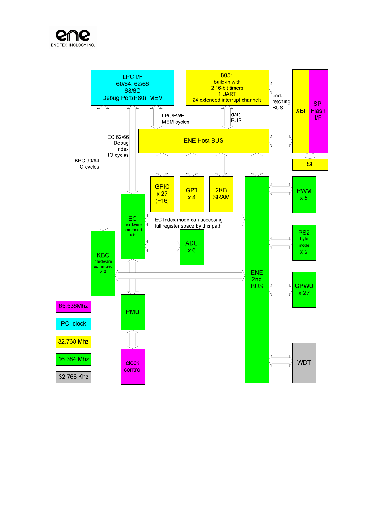
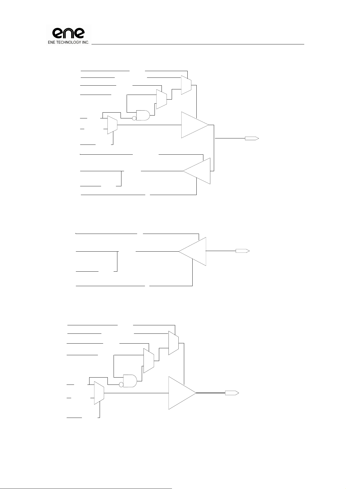
1.2 Block Diagram
KB3700 Keyboard Controller Datasheet
Copyright©2006, ENE Technology Inc. 7
Page 8

KB3700 Keyboard Controller Datasheet
2. Pin Assignment and Description
2.1 Pin List
No. Pin Name GPIO Alt. Output. Alt. Input Default Reset IOCELL
1 GPIOE0 GPIOE0 BQC04HU
2 GPIOE1 GPIOE1 BQC04HU
3 GPIOE2 GPIOE2 BQC04HU
4 GPIOE3 GPIOE3 BQC04HU
5 SERIRQ BCC16H
6 GPIO00 GPIO00 GA20 BQC04HU
7 LFRAME#
8 LAD3 BCC16H
9 GPIO01 GPIO01 KBRST# BQC04HU
10 GPIO02 GPIO02 PLLCLK_REF2 BQC04HU
11 LAD2 BCC16H
12 LAD1 BCC16H
13 VCC VCC
14 LAD0 BCC16H
15 GND GND
16 GPIO03 GPIO03 PCICLK BCC16H
17 GPIOE4 GPIOE4 BQC04HU
18 GPIOE5 GPIOE5 BQC04HU
19 GPIOE6 GPIOE6 BQC04HU
20 GPIOE7 GPIOE7 BQC04HU
21 GPIO04 GPIO04 PCIRST# BCC16H
22 GPIO05 GPIO05 SCI# BQC04HU
23 GPIO06 GPIO06 PWM0/E51_TXD BCC16H
24 GPIO07 GPIO07 PWM1/E51_CLK E51_RXD BCC16H
25 GPIO08 GPIO08 PWM2 BCC16H
26 GPIO09 GPIO09 PWM3 BCC16H
27 GPIO0A GPIO0A PWM4 BCC16H
28 GPIO0B GPIO0B E51_TMR0 BQC04HU
29 GPIO0C GPIO0C E51_TMR1 BQC04HU
30 GPIO0D GPIO0D E51_TXD ECRST# BQC04HU
31 GPIO0E GPIO0E PLLCLK32 E51_INT0 ECRST# BQC04HU
32 GPIO0F GPIO0F POR E51_INT1 BQC04HU
33 GPIOE8 GPIOE8 BQC04HU
34 AD3 IQA
35 AD4 IQA
36 AD5 IQA
37 GPIO10 GPIO10 BQC04HU
38 AD0 IQA
39 AD1 IQA
40 AD2 IQA
41 AVCC AVCC
42 AGND AGND
43 GPIO11 GPIO11 PSCLK1 PSCLK1 BQC04HU_10K
44 GPIO12 GPIO12 PSDAT1 PSDAT1 BQC04HU_10K
BCC16H
Copyright©2006, ENE Technology Inc. 8
Page 9
45 GPIO13 GPIO13 PSCLK2 PSCLK2 BQC04HU_10K
46 GPIO14 GPIO14 PSDAT2 PSDAT2 BQC04HU_10K
47 GPIO15 GPIO15 TEST_CLK BQC04HU
48 GPIO16 GPIO16 TP_CLK_TEST BQC04HU
49 GPIOEC GPIOEC BQC04HU
50 GPIOED GPIOED BQC04HU
51 GPIOEE GPIOEE BQC04HU
52 GPIOEF GPIOEF BQC04HU
53 GPIO17 GPIO17 CLK TP_PLL_TEST BQC04HU
54 GPIO18 GPIO18 CLK32MHz(8051) TP_ISP_MODE BQC04HU
55 GPIO19 GPIO19 CLK16MHz(peri) TP_IO_TEST BQC04HU
56 GPIO1A GPIO1A CLK32MHz(WDT BQC04HU
57 GPIO1B GPIO1B BQC04HU
58 SPIDI BCC16H
59 SPIDO BCC16H
60 SPICLK BCC16H
61 SPICS# BCC16H
62 VCC VCC
63 VCC18 VCC18
64 GND GND
KB3700 Keyboard Controller Datasheet
2.2 I/O Buffer Table
IO Name Descriptions Applications
BQC04HU Schmitt trigger, 2~4mA Output / Sink Current, with , Input / Output / Pull Up Enable GPIO
BQC04HU_10K Schmitt trigger, 2~4mA Output / Sink Current, with , Input / Output / 10KΩ Pull Up Enable GPIO
BCC16H 8~16mA Output / Sink Current , 5 V Tolerance, Input / Output Enable LPC Interface
IQA Mixed mode IO, ADC Enable, with GPI, 2~4mA Sink Current, Input Enable ADC, GPIN
2.3 I/O Buffer Characteristic Table
IO Name
Port
BQC04HU V V V V V 40K (typ.)
BQC04HU_10K
BCC16H V V V V V V 8~16mA
IQA V V V V
IO I O OE IE AE 5VTor PE
V V V V V 10K (typ.)
Output / Sink
Current
2~4mA
2~4mA
2.4 I/O Naming Convention
I IO Buffer Input
O IO Buffer Output
OE IO Buffer Output Enable
IE IO Buffer Input Enable
PE IO Buffer Pull High Enable
AE IO Buffer Analog mode Enable(AE > OE)
Q Schmitt Trigger
H 5V Tolerance
Copyright©2006, ENE Technology Inc. 9
Page 10
1
2
3
4
5
6
7
8
9
10
11
Embedded Controller
(hardware EC Space)
12
General Purpose Wake
-
up
(hardware EC Space)
KB3700 Keyboard Controller Datasheet
3. Pin Descriptions
3.1 Hardware trap
Hardware trap pins will latch the external signal levels at the rising edge of ECRST#. Either a High
or Low value will be stored internally to serve as control signals as described below.
For normal application, there is no application component required for selecting the normal mode
because KB3700 build-in internal pull up resistor to select the right operation mode.
After KB3700 booted, the pull up resistor may be disabled by GPIO register setting.
Pin name 64 Pins
TP_TEST
48
(GPIO16)
TP_PLL
53
(GPIO17)
TP_TEST: Clock Test Mode (for testing and ISP Mode)
Low: Clock Test Mode Enable. (all internal logic will use GPIO15 as clock
source)
TP_PLL: PLL Test Mode (for testing)
LOW: PLL Test Mode Enable
GPIO0E is PLL 32MHz clock output.
GPIO0F is Power On Reset output.
HW Strap Description
HIGH: Normal operation (MUST, Power-On Default)
TP_ISP
54
(GPIO18)
TP_IO
55
(GPIO19)
TP_ISP: ISP Mode (for programming external SPI flash)
LOW: ISP Mode Enable
HIGH: Normal operation in not ISP mode (MUST, Power-On Default)
TP_IO: IO Test Mode (for testing)
LOW: IO Test Mode Enable
HIGH: Normal operation (MUST, Power-On Default)
4. Module Descriptions
The following table gives the corresponding memory map for accessing. Each module will be
described detail in the individual sections.
No. Abbreviation
Flash Program space mapped to system BIOS 0000h~F3FFh 61K
XRAM Embedded SRAM F400h~FBFFh 2K
GPIO General Purpose IO (include ADC, DAC) FC00h~FC7Fh 128
KBC Keyboard Controller FC80h~FC9Fh 32
PWM Pulse Width Modulation FE00h~FE1Fh 32
GPT General Purpose 16-bit timer FE50h~FE6Fh 32
WDT Watchdog Timer FE80h~FE8Fh 16
LPC Low Pin Count FE90h~FE9Fh 16
XBI X-BUS Interface FEA0h~FECFh 48
PS2 PS2 FEE0h~FEFFh 32
EC
GPWU
Device Full Name Address Range Size (Byte)
FF00h~FF1Fh 32
FF20h~FE7Fh 96
1K
Copyright©2006, ENE Technology Inc. 10
Page 11
GPIOD00
4.1 Chip Architecture
4.1.1 Power Planes
There are 2 power planes in this chip. One is used for all logic, the other is used for Analog
parts (ADC).
4.1.2 Clock Domains
There are 4 clock domain in KB3700.
Flash chip interface clock. The clock default in 16MHz, and can be to 32MHz or 64MHz.
8051 / XBI use high clock (setting in CLKCFG, FF0Dh), ranges from 22~4MHz.
WDT uses 32.768KHz clock. WDT default use internal 32KHz clock. The WDTCFG bit 7
options can switch WDT clock to external 32KHz clock oscillator.
Other peripherals (GPWU, PWM,.) use low clock (setting in CLKCFG, FF0Dh), ranges
from 8~2MHz.
4.1.3 Reset Domains
KB3700 Keyboard Controller Datasheet
This chip builds in power on reset. There is also a input reset signal (ECRST#) for global reset.
WDT reset can reset almost all logic, except WDT and GPIO modules. The WDT reset can be
set to only reset 8051 by EC register (PXCFG, FF14h).
There is additional 8051 reset source from EC register (PXCFG, FF14h).
4.2 GPIO
4.2.1 GPIO Functional Description
Multi-function pin Output Function Selection (FS) bit = 0, is set for GPIO Output Function,
and FS bit = 1, is set for Alternative Output. The alternative input function is enabled by Input
Enable register (IE), and is not affected by FS register.
Offset
00
~
03
10
~
15
20
~
Register
Abbreviation
GPIOFS00
GPIOFS08
GPIOFS10
GPIOFS18
GPIOOE00
GPIOOE08
GPIOOE10
GPIOOE18
GPIOEOE0
GPIOEOE8
GPIOD08
Register Full Name
Bit Attr Description
GPIO 00~1B Output Function Selection (0: GPO, 1: Alternative Output)
00h: GPIOFS00 for GPIO00~07 0
7~0 R/W
GPIO 00~1B Output Enable (0: Output Disable, 1: Output Enable)
7~0 R/W
GPIO 00~1B Data Output
7~0
R/W
01h: GPIOFS08 for GPIO08~0F 0
02h: GPIOFS10 for GPIO10~17 0
03h: GPIOFS18 for GPIO18~1B 0
10h: GPIOOE00 for GPIO00~07 0
11h: GPIOOE08 for GPIO08~0F 0
12h: GPIOOE10 for GPIO10~17 0
13h: GPIOOE18 for GPIO18~1B 0
14h: GPIOEOE0 for GPIOE0~7 0
15h: GPIOEOE8 for GPIOE8~F (GPIOE9~A is N.A.) 0
20h: GPIOD00 for GPIO00~07 0
Def Bnk
FC
FC
FC
Copyright©2006, ENE Technology Inc. 11
Page 12

30
~
36
40
~
45
50
~
53
60
~
66
GPIOIN00
GPIOIN08
GPIOIN10
GPIOIN18
GPIOEIN0
GPIOEIN8
GPIADIN
GPIOPU00
GPIOPU08
GPIOPU10
GPIOPU18
GPIOEPU0
GPIOEPU8
GPIOOD00
GPIOOD08
GPIOOD10
GPIOOD18
GPIOIE00
GPIOIE08
GPIOIE10
GPIOIE18
GPIADIE
KB3700 Keyboard Controller Datasheet
21h: GPIOD08 for GPIO08~0F 0
22h: GPIOD10 for GPIO10~17 0
23h: GPIOD18 for GPIO18~1B 0
24h: GPIOED0 for GPIOE0~7 0
25h: GPIOED8 for GPIOE8~F (GPIOE9~A is N.A.) 0
GPIO 00~1B Input Status
30h: GPIOIN00 for GPIO00~07
31h: GPIOIN08 for GPIO08~0F
32h: GPIOIN10 for GPIO10~17
7~0 R/W
GPIO 00~1B Pull Up Enable
R/WC
7~0
1
GPIO 00~1B Open Drain Enable
7~0 R/W
GPIO 00~1B Input Enable
7~0 R/W
GPIO MISC
33h: GPIOIN18 for GPIO18~1B
34h: GPIOEIN0 for GPIOEIN0~7
35h: GPIOEIN8 for GPIOEIN8~F (GPIOEIN9~A is N.A.)
36h: GPIAD0 for GPIAD0~5
40h: GPIOPU00 for GPIO00~07 0
41h: GPIOPU08 for GPIO08~0F 20
42h: GPIOPU10 for GPIO10~17 E0
43h: GPIOPU18 for GPIO18~1B 03
44h: GPIOEPU0 for GPIOE0~7 0
45h: GPIOEPU8 for GPIOE8~F (GPIOE9~A is N.A.) 0
50h: GPIOOD00 for GPIO00~07 0
51h: GPIOOD08 for GPIO08~0F 0
52h: GPIOOD10 for GPIO10~17 0
53h: GPIOOD18 for GPIO18~1F 0
60h: GPIOIE00 for GPIO00~07 0
61h: GPIOIE08 for GPIO08~0F 20
62h: GPIOIE10 for GPIO10~17 E0
63h: GPIOIE18 for GPIO18~1B 03
64h: GPIOEIN0 for GPIOE0~7 0
65h: GPIOEIN8 for GPIOE8~F (GPIOE9~A is N.A.) 0
66h: GPIAD0 for GPIAD0~5 0
FC
0
FC
FC
FC
70 GPIOMISC
7~2 RSV 0
FC
1 R/W Select GPIO07 as E51_CLK. 0
0 R/W Select GPIO06 as E51_TXD. 0
Copyright©2006, ENE Technology Inc. 12
Page 13
4.2.2 GPIO Input / Output Control Structure
GPIOFS
Alt. Output Enable
GPIOOD
GPIOD
Alt. Output
GPIOFS
GPIOOE
0
1
Pull up Enable
GPIOPIN
Alt Input
0
1
IE
1
0
Output Buffer
Input Buffer
IE
KB3700 Keyboard Controller Datasheet
OE
IO PIN
PE
PE
GPIOPIN
Alt Input
IE
Input Buffer
INPUT PIN
GPIOFS
Alt. Output Enable
GPIOOD
GPIOOE
0
1
1
0
GPIOD
Alt. Output
0
1
GPIOFS
Copyright©2006, ENE Technology Inc. 13
OE
OUTPUT PIN
Output Buffer
Page 14

just emulates the function.
Always return 00h
Read the output port of 8042 P2. Because there is no real 8042 in the chip, this command
just emulates the function.
will just emulate the function and set/clear GA20 based on data bit 1.
Auxiliary data
Always return 00h
4.3 KBC
4.3.1 KBC Functional Description
a. IO 60h: KBC Data Input Register (KBDIN):
When the host writes I/O ports 60h and 64h, the data is stored in KBDIN. At the same
time, the input buffer full flag (IBF bit in KBSTS) is set. The input data stored in KBDIN is
directly fetched by the command processing logic and IBF is also cleared automatically
b. I/O 60h: KBC Data Output Register (KBDOUT)
The data responded to the host is generated by the hardware circuit. The data is pushed
into KBDOUT and the output buffer full flag (OBF bit in KBSTS) is set automatically.
KB3700 can be configured to generate interrupts to the host when OBF is set. OBF is
automatically cleared after that the host reads KBDOUT (through I/O port 60h)
c. I/O 64h: KBC Status Register (KBSTS)
The host read it through I/O port 64h. The bit format of this register is as follows:
Status Bit
7 Parity Error PS/2 Bus parity error.
6 General Timeout PS/2 Bus timeout.
5 Aux OBF KBDOUT data is from PS/2 auxiliary device.
4 Uninhibited Keyboard is not inhibited.
3 A2 Address of the previous write cycle.
2 System Flag POST of the system is finished.
1 IBF Input Buffer Full flag.
0 OBF Output Buffer Full flag.
Name Description
KB3700 Keyboard Controller Datasheet
.
.
d. Hardware Processed Command
The following standard commands are processed by hardware directly.
Value Command Description
20h
D0h
D2h
D3h
E0h
FEh
Read Command Byte
Read P1
Read P2
Write P2
Write KB Output Buffer
Write AUX Output Buffer
Read Test Input
KB Reset This command generates a 6us low pulse on KBRST#.
Read the command byte of KBC
Response Command byte
Read the input port of 8042 P1. Because there is no real 8042 in the chip, this command
Response
Response Bit1 is the status of GA20
Write the output port of 8042 P2. Because there is no real 8042 in the chip, this command
Argument Bit1 is the status of GA20
Write data into KBDOUT as if it comes from the keyboard.
Argument Keyboard data
Write data into KBDOUT as if it comes from the auxiliary device.
Argument
Read the test inputs T0 and T1 of 8042. Because there is no real 8042 in the chip, this
command will just emulate the function.
Response
C0h
D1h
Copyright©2006, ENE Technology Inc. 14
Page 15

KB3700 Keyboard Controller Datasheet
4.3.2 KBC Registers Descriptions (Base Address = FC80h, 32 bytes)
Offset
80h KBCCB
81h KBCCFG
82h KBCIF
83h KBCHWEN
84h KBCCMD
85h KBCDAT
86h KBCSTS
Register
Abbreviation
Register Full Name
Bit Attr Description
KBC Command Byte (KBC command 20h/60h)
7 RSV
6 R/W Scan Code Conversion
5 R/W Auxiliary Device Disable
4 R/W Keyboard Device Disable
3 R/W Inhibit Override
2 R/W System Flag
1 R/W IRQ12 Enable
0 R/W IRQ1 Enable
KBC Configuration
7 R/W Keyboard Lock Enable
6 R/W Fast Gate A20 Control
5~4 RSV
3 R/W Keyboard Lock
2 RSV
IBF Interrupt Enable.
1 R/W
0 R/W
KBC Interrupt Pending Flag
7~3 RSV
2 R/WC1
1 R/WC1 IBF interrupt pending flag
0 R/WC1 OBF interrupt pending flag
KBC Hardware Command Enable
7 R/W FEh: KB Reset command processed by hardware
6 R/W E0h: read test input command processed by hardware
5 R/W D3h: write AUX output buffer
4 R/W D2h: write KB output buffer
3 R/W D1h: write P2 command processed by hardware
2 R/W D0h: read P2 command processed by hardware
1 R/W C0h: read P0 command processed by hardware
0 R/W 20h: read command byte processed by hardware
KBC Command Buffer
7~0 RO The data written to I/O port 64h will be stored in this register.
KBC Data Input / Output Buffer
7~0 R/W
KBC Host Status
7 R/W
6 R/W
5 R/W Auxiliary Data Flag
4 RO Uninhibited
3 RO Address (A2)
2 RO System Flag
1 R/WC1 IBF, write IBF = 1 to clear IBF
0 R/WC1 OBF, write KBCDAT will set OBF to 1. Write OBF = 1 to clear OBF
This bit enables KBC to generate interrupt to the 8051 at the rising edge of
IBF, when the KBC command being received will be bypassed to firmware for
processing.
OBF Interrupt Enable.
This bit enables KBC to generate interrupt to the core processor at the falling
edge of OBF.
KBC firmware mode in processing flag,
Exit KBC firmware mode and re-enable hardware mode by writing 1
Writing to this register will cause the output buffer full flag OBF to be set. The
host can read this register through I/O port 60h.
Parity Error.
When PS/2 protocol has a parity error, this bit will be set to high. This bit is
also used as port indicator for PS/2 active multiplexing mode.
TimeOut.
When PS/2 protocol has a timeout error, this bit will be set to high. This bit is
also used as port indicator for PS/2 active multiplexing mode.
4.4 PWM
Def Bnk
40 FFh
0 FFh
0 FFh
0 FFh
0 FFh
0 FFh
0 FFh
Copyright©2006, ENE Technology Inc. 15
Page 16

FE
KB3700 Keyboard Controller Datasheet
4.4.1 PWM Functional Description
There are 5 PWM channels with 8-bit resolution.
PWM2,3,4 are controlled by the same configuration register in PWMCFG2 with 6 bit clock
prescaler.
The PWM Cycle Length defines the PWM cycle time in setting clock source. The PWM High
Period Length defines the PWM pulse high period length, should be less than Cycle Length
.
Here is the formula of PWM duty cycle.
Duty Cycle = (PWM High Period Length+1)/(PWM Cycle Period Length+1) *100%
Please note the following case:
Condition PWM Output
H > C Always 1 (High)
H and C=0x00 Always 1 (High)
H=0x00, C=0xFF A short pluse
H=0xFF, C=0x00 Always 1 (High)
1. Where H means High Period Length (PWMHIGH) ; C means Cycle Period Length (PWMCYCL)
Please refer to the following PWM register description.
2. To force PWM output Low, please force this pin to be GPIO mode and output low.
4.4.2 PWM Registers Descriptions (Base address_FE00h, 16 bytes)
Offset
0 PWMCFG
1 PWMHIGH0
2
3 PWMHIGH1
4 PWMCYCL1
5
6
7
Register
Abbreviation
PWMCYCL0
PWMCFG2
PWMCFG3
PWMCFG4
Bit Attr
PWM Configuration 0
PWM1 clock source selection
0: 1us
7~6 R/W
5 RSV 0
4 R/W PWM1 Enable 0
3~2 R/W
1 RSV 0
0 R/W PWM0 Enable 0
PWM0 High Period Length 0
7~0 R/W The High Period Length of PWM should be small than Cycle Length. 0
PWM0 Cycle Length 0
7~0 R/W The Cycle Length of a PWM cycle, includes high and low Length.
PWM1 High Period Length 0
7~0 R/W The High Period Length of PWM should be small than Cycle Length. 0
PWM1 Cycle Length 0
7~0 R/W The Cycle Length of a PWM cycle, includes high and low Length.
PWM Configuration 2, 3, 4
7 R/W PWM2, 3, 4 Enable
6 R/W
1: 64us
2: 256us
3: 4ms
PWM0 clock source selection
0: 1us
1: 64us
2: 256us
3: 4ms
PWM prescaler Clock Select
0: peripheral clock(by clock setting in EC CLKCFG(FF0Dh)
1: 1MHz clock(recommend set this bit to fixed clock in different clock setting)
Register Full Name
Description
Def Bnk
0
FE
0
FE
FE
FE
FE
0
Copyright©2006, ENE Technology Inc. 16
Page 17

5~0 R/W The 6-bit prescaler for PWM by selected clock.
8
9
A
B
C
D
PWMHIGH2
PWMHIGH3
PWMHIGH4
PWMCYC2
PWMCYC3
PWMCYC4
PWM2, PWM3, PWM4 High Period Length
7~0 R/W High byte (8 bits)
PWM2, PWM3, PWM4 Cycle Length
7~0 R/W High byte (8 bits)
KB3700 Keyboard Controller Datasheet
4.5 GPT
4.5.1 GPT Functional Description
There are 4 GPTs in KB3700. 2 GPTs are 16-bit, and the other 2 are 8-bit. ALL base on
30.516 us (32.768KHz) clock, and are independent on clock setting in EC register.
GPT0 and GPT1 are 8-bit timer.
GPT2 and GPT3 are 16-bit timer.
4.5.2 GPT Register Descriptions (Base address = FE50h, 16 bytes)
Offset
50
51 GPTPF
53 GPT0
55
56
57
58
59
Register
Abbreviation
GPTCFG
GPT1
GPT2H
GPT2L
GPT3H
GPT3L
Bit Attr
GPT Configuration
7~5 RSV
4 R/W GPT test mode, the GPT base clock will be system clock
3 R/W Enable GPT3 counting and GPT3 interrupt
2 R/W Enable GPT2 counting and GPT2 interrupt
1 R/W Enable GPT1 counting and GPT1 interrupt
0 R/W Enable GPT0 counting and GPT0 interrupt
GPT Pending Flag 0
7 WO GPT3 write 1 to restart 0
6 WO GPT2 write 1 to restart
5 WO GPT1 write 1 to restart
4 WO GPT0 write 1 to restart
3 R/WC1 GPT3 Interrupt Pending Flag
2 R/WC1 GPT2 Interrupt Pending Flag
1 R/WC1 GPT1 Interrupt Pending Flag
0 R/WC1 GPT0 Interrupt Pending Flag
GPT0 Count Value
7~0 R/W
GPT1 Count Value
7~0 R/W
GPT2 Count Value
7~0 R/W
GPT3 Count Value
7~0 R/W
After GPT0 reach this value and interrupt will occur and
GPT0 reset and counting from zero again.
After GPT1 reach this value and interrupt will occur and
GPT1 reset and counting from zero again.
After GPT2 reach this value and interrupt will occur and
GPT2 reset and counting from zero again.
After GPT3 reach this value and interrupt will occur and
GPT3 reset and counting from zero again.
Register Full Name
Description
0 FE
0 FE
Def Bnk
0 FE
FE
FE
0
0
FE
0
0
FE
0
0
FE
0
0
Copyright©2006, ENE Technology Inc. 17
Page 18

5 R/W
KB3700 Keyboard Controller Datasheet
4.6 SPI/ISP Device Interface
4.6.1 SPI/ISP Functional Description
SPI includes several functions, as follows,
1. 2 code segments for 8051.
2. Performance improvement: instruction sustain fetch, and pre-fetch
3. flash write protection
4. ISP should be enabled by hardware trap pin during hardware reset.
1. The ISP packet format: If bit 7th of 1st byte is 1 means write packet, otherwise means
read.
1. ISP write : [1000_XXXX] [WDATA]
2. ISP read : [ 0000_XXXX] [RDATA]
4.6.2 SPI Registers Descriptions (Base address = FE70h, 16 bytes)
Offset
A0h XBISEG0
A4h XBIXIOEN
A5h XBICFG
Register
Abbreviation
Bit Attr
8051 Address Segment 0 (0000h-3FFFh) Mapping Configuration
7 R/W Enable 8051 Code Space SEG0 Remapping
5~0 R/W XBI address = XBISEG0*16k + 8051 address [13:0]
8051 Address Segment 1 (4000h-7FFFh) Mapping Configuration
7 R/W Enable 8051 Code Space SEG1 Remapping A1h XBISEG1
5~0 R/W XBI address = XBISEG1*16k + 8051 address [13:0]
XBI XIO Enable
7~0 R/W Enable related XIO channel (Only 4 channels)
XBI Configuration
7 R/W Enable XBI BUS IO buffer pull up
6 R/W Enable 8051 sustain instruction fetch
4 RO Enable WR# to flash
3 R/W
2-0 R/W RD# and WR# command clock count= [2:0]
XBI E51CS# Configuration
7 R/W Enable E51CS# address 16~64K
6 R/W
Enable extend SELMEM# and SELE51# 1 clock for RD# and WR# setup
Register Full Name
Description
Def Bnk
0 FEh
0 FEh
0 FEh
07h FEh
Enable Reset 8051 and XBI Segment Setting (XBISEG0~3)
A6h XBICS
A7h XBIWE
A8h
A9h
AAh
ABh SPIDAT
ACh SPICMD
Copyright©2006, ENE Technology Inc. 18
SPIA0
SPIA1
SPIA2
4 R/W
3 RSV
2 R/W Enable STOP and IDLE state let XBI state machine go to initial state.
1 R/W
0 R/W Select XIO select to SELIO# (set 1) or SELIO2# (set 0).
XBI Write Enable
7-0 WO
XBI SPI Flash Address
7-0 R/W
XBI SPI Flash Output / Input Data
7-0 R/W
XBI SPI Flash Command
reset XBI registers A0~A3h(bank select) when WDT / Wakeup / EC
Register reset 8051.
Enable EHB Fast Access
A enhanced option to speed up EHB performance.
Write 00h to reset all rest mode.
Write A3h to enable flash write cycles.
Write C5h to SRAM test.
SPIA0 = A7~0
SPIA1 = A15~8
SPIA2 = A22~16
Output(write SPIDAT) / Input(read SPIDAT) data to/from SPI flash
interface.
04h FEh
0 FEh
0 FEh
0 FEh
0 FEh
Page 19

ADh SPICFG
AEh SPIDATR
AFh SPICFG2
KB3700 Keyboard Controller Datasheet
The issued SPI command to SPI flash chip. The write to this register will
start the SPI accessing, so that the SPIA2~0 and SPIDAT should be ready
before SPICMD is written.
SPICMD support command :
01h Write Status Register
02h Byte Program
03h Read
04h Write Disable
7-0 R/W
SPI Flash Configuration / Status
7 R/W Enable DPLL for ISP mode
6 R/W SPI Flash Offset Read Command Enable. (32h)
5 R/W
4 R/W
3 R/W
2 R/W
1 RO
0 R/W Enable SPICMD follow with a SPI status check until Busy flag cleared.
SPI Flash Output Data for Read Compare
7-0 RO Output data to SPI flash interface.
SPI Flash Configuration 2
7-4 RSV Reserved.
3-0 R/W SPI Offset / Short Read Command high nibble.
05h Read Status Register
06h Write Enable
0Bh High Speed Read
20h Sector Erase (SST)
50h Enable Write Status Register (SST)
52h Block Erase (SST)
60h Chip Erase (SST)
C7h Chip Erase (PCM, NexFlash)
D7h Sector Erase (PCM)
D8h Block Erase (PCM, NexFlash)
SPI Flash Short Read Command Enable. (31h, 30h)
A23~16 will not be used. A16 = 1 if 31h command. A16=0 if 30h command.
The address phase will only contain A15~0, and don't care fast mode
enable bit of SPICFG bit 2.
SPICS# force output low.
After set this bit, the protocol will control by firmware. The SPICMD will
output to SPI BUS each time the write operation to SPICMD.
The SPIDAT will store the read operation data from SPI BUS.
SPICMD write enable.
Enable SPICMD write action to start SPI flash protocol accessing.
Enable SPI Flash Dummy Byte for Read Command.
Enable SPI flash read by 8051 instruction by Fast Mode (High Speed
Read) 0Bh command.
SPI flash accessing in progress status.
Use this bit to check if the SPI accessing is finished or not.
00 FEh
0 FEh
0 FEh
4.6.3 ISP Registers Descriptions (8 bytes)
Offset
0
1
2
3 ISPDAT
4 ISPCMD
Copyright©2006, ENE Technology Inc. 19
Register
Abbreviation
ISPIA0
ISPIA1
ISPA2
Bit Attr
ISP SPI Flash Address
7-0 R/W
ISP SPI Flash Output / Input Data
7-0 R/W
ISP SPI Flash Command
SPIA0 = A7~0
SPIA1 = A15~8
SPIA2 = A22~16
Output(write SPIDAT) / Input(read SPIDAT) data to/from SPI flash
interface.
Register Full Name
Description
Def
0
0
0
Page 20

start the SPI accessing, so that the SPIA2~0 and SPIDAT should be ready
Fast Mode (High Speed Read) 0Bh
protocol.
5 ISPCFG
6 ISPDATR
KB3700 Keyboard Controller Datasheet
The issued SPI command to SPI flash chip. The write to this register will
before SPICMD is written.
SPICMD support command :
01h Write Status Register
02h Byte Program
03h Read
04h Write Disable
7-0 R/W
ISP SPI Configuration / Status
7 ~ 5 R/W
4 R/W
3 R/W
2 R/W
1 RO
0 R/W Enable SPICMD follow with a SPI status check until Busy flag cleared.
ISP SPI Flash Output Data for Read Compare
7-0 RO Output data to SPI flash interface.
05h Read Status Register
06h WriteEnable
0Bh High Speed Read
20h Sector Erase (SST)
50h Enable Write Status Register (SST)
52h Block Erase (SST)
60h Chip Erase (SST)
C7h Chip Erase (PCM, NexFlash)
D7h Sector Erase (PCM)
D8h Block Erase (PCM, NexFlash)
SPICS# force output low.
After set this bit, the protocol will control by firmware. The SPICMD will
output to SPI BUS each time the write operation to SPICMD.
The SPIDAT will store the read operation data from SPI BUS.
SPICMD write enable.
Enable SPICMD write action to start SPI flash protocol accessing.
SPI flash read by 8051 instruction by
SPI flash accessing in progress status.
Use this bit to check if the SPI accessing is finished or not.
0
0
ISP SPI ISP RS232 Baud Rate Setting
In ISP mode, 8051_SFR(SCON2) always 0
7-0 WO
7
refer to the yellow part, and read operation please refer to the green part.
ISPSCON3
***
7~4 RSV
3~0 RO
*** Please note, ISPSCON3 register gives different bitmap definition according to access. For write operation, please
write this reg to program 8051_SFR(SCON3)
Default: SCON3 = 0x89, baud-rate = 57600 (while 8051 clk = 8Mhz)
set SCON3 = 0x45 for baud-rate =115200 (while 8051 clk = 8Mhz)
Reserved
SPI Offset / Short Read Command high nibble.
0
3
Copyright©2006, ENE Technology Inc. 20
Page 21

FE
KB3700 Keyboard Controller Datasheet
4.7 WDT
4.7.1 WDT Functional Description
WDT timer clock uses 32.768 KHz oscillator clock and base unit is 64ms.
WDT register can only be reset by power on reset and ECRST#.
WDT range is between 64 ms to 16 seconds.
WDT reset time is between 128ms to 32 seconds.
WDT reset can reset all logic in the chip, except GPIO registers. Thus, the GPIO setting can
be preserved after WDT reset occurred. The WDT reset can optionally be set only to reset 8051
logic in EC register space.
4.7.2 WDT Registers Descriptions (Base address = FE80h, 16 bytes)
Offset
Register
Abbreviation
Bit Attr
WDT Configuration
WDT Extended Bits Enable
0: WDT is 20-bit timer (normal setting).
7 R/W
1: WDT is 24-bit timer (setting for PLLLOW in STOP mode).
If EC CLKCFG.7 (PLLLOW Enable) is set, the WDT clock will become PLL
output clock automatically. Set this bit to 1 before enter STOP mode to let WDT
become 24-bit timer by 1~2MHz PLL output clock.
Register Full Name
Description
Def Bnk
80 WDTCFG
81 WDTPF
82 WDTCNT
6~3 R/W
2 R/W
1 R/W Enable WDT interrupt (WDT reset warning)
0 R/W
WDT Pending Flag
7~5 RSV
1
R/WC1
0
R/WC1
WDT 8-bit Count Value (for Watch Dog Timer reset system)
7~0 R/W
Force to disable WDT by writing 1001b to this field.
Write 1011b to set WDT be shorter timer. (Enable WDT shorter test mode).
Write 1111b to disable WDT shorter test mode.
WDT Clock Selection for testing
0: WDT clock is from WDT Clock Selection 2 (normal setting).
1: WDT clock is PLL output / 2 (i.e. 16MHz as PLL output 32MHz, maybe
stopped at STOP mode. This option is only for testing).
Enable WDT reset, and reset WDT timer,
the WDT timer and 2 pending flags will be reset and count from zero again.
If the WDT and reset after a interrupt occurred, the next interrupt will occurred
after 16 seconds.
WDT interrupt pending, WDT half timeout flag. If this bit is set, the following
WDT timeout event will cause a WDT reset signal to system.
WDT reset event pending flag (the last WDT reset was ever happened),
WDT reset will assert if WDT count to WDT and WDT interrupt is pending.
After WDT counts to this value the half of WDT/2 , the interrupt will occur. The
WDT timer unit is 64ms.
0 FE
0 FE
0 FE
83
84
85
Copyright©2006, ENE Technology Inc. 21
WDT19_12
WDT11_04
WDT03_00
WDT Counter Value(for testing)
0
0 RO Only for WDT testing.
Page 22

4.8 LPC
4.8.1 LPC / FWH Functional Description
There are 5 address ranges on LPC/FWH interface will be responded by KB3700 EC.
1. Keyboard controller I/O ports: 60h, 64h
2. Embedded controller I/O ports: 2 programmable I/O ports (default 62h/66h and 68h/6Ch)
3. EC I/O Index and Data Ports: Through which the system host can access KB3925
internal registers more efficiently than through EC commands F0h/F1h. The EC I/O Index
and Data Ports are two 8-bit registers with base address defined in FE92h and FE93h.
Default Index Port ={002Dh, 002Eh}, Data port =002Fh.
4. LPC/FWH memory access.
5. Extended LPC write byte: can be programmed to port 80 and generate interrupt to 8051.
4.8.1.1 LPC Decoding IO Ports
The keyboard I/O ports are 60h/64h, while the EC I/O ports are programmable in
LPCEBA (FE98h, FE99h). The enable/disable of I/O ports decoding on LPC bus can be
KB3700 Keyboard Controller Datasheet
configured individually via register LPCCFG (FE95h).
4.8.1.2 LPC Decoding Memory Space
Memory Setting (LPCFWH bit 7,6)
00 256k (default)
01 512k
10 1M
11 2M
4.8.2 LPC Registers Descriptions (Base address = FE90h, 16 bytes)
Offset
90h LPCSTAT
91h LPCSIRQ
Register
Abbreviation
LPC Status (Internal Use Only)
7~2 RSV
1 R
0 RSV
LPC SIRQ Configuration
7 R/W Enable don't care A22 of FWH memory cycle
6 R/W Enable SCI SIRQ
Bit Attr
Memory Size Decoded BIOS Address
000C_0000 – 000F_FFFF
FFFC_0000 – FFFF_FFFF
000C_0000 – 000F_FFFF
FFF8_0000 – FFFF_FFFF
000C_0000 – 000F_FFFF
FFF0_0000 – FFFF_FFFF
000C_0000 – 000F_FFFF
FFE0_0000 – FFFF_FFFF
Register Full Name
Description
LPC SIRQ is current in quiet/continuous mode
1: quiet mode
0: continuous mode
Def Bnk
0 FEh
0 FEh
Copyright©2006, ENE Technology Inc. 22
Page 23

92h
LPCIBAH
93h
94h LPCFWH
95h LPCCFG
96h
97h
98h
99h
9Ah LPC_2EF
9Ah LPC_2EF
9Bh
9Ch LPC_2F_DATA
9Dh LPC68CFG
LPCIBAL
LPCXBAH
LPCXBAL
LPCEBAH
LPCEBAL
KB3700 Keyboard Controller Datasheet
5 R/W Enable IRQ12 SIRQ
4 R/W Enable IRQ1 SIRQ
SCI Serial IRQ channel
0: no
3 – 0 R/W
LPC Index IO Base Address
7 – 0 R/W
LPC FWH Configuration 0
7 – 6 R/W
5 R/W Enable FWH memory cycle
4 R/W Enable FWH IDSEL check
3 – 0 R/W FWH ID
LPC Configuration
7 R/W Enable LPC memory write protection (including FWH)
6 R/W Enable index IO port
5 R/W Enable KBC IO port: 60h, 64h
4 R/W Enable Extended IO port (IO write only)
3 R/W Enable EC IO port
2 R/W Enable LPC memory cycle (not including FWH)
1 R/W Enable SIRQ fixed in continuous mode
0 R/W Enable LPC CLKRUN#
LPC Extended IO Base Address
Only LPC byte write is supported
LPC EC IO Base Address
LPCEBAL bit 0 and bit 1 are not ignored for decoding
Address 2EF decoding and control in LPC(Internal Use Only)
Address 2EF decoding and control in LPC(NOTE: Internal Use Only)
7~4 RSV
3 R Decode IO(0x002F): 0:read_io_2f, 1:write_io_2f
2 R/RW
1 R/W Enable interrupt of read/write_io(2f)
0 R/W Enable decode read_io(2e), read/write_io(2f)
7~0 RSV
LPC_2F_DATA
7~0 RO Read data for read_cycle_IO(2F)
LPC 68/6Ch IO Configuration
7 R/W Enable LPC I/F decode IO 68h, 6Ch
RSV
6~2
1:IRQ1
2:SMI#
3:IRQ3
…
15:IRQ15
EC index mode IO port base address.
The address should be 4 bytes align.
Memory Size (both for LPC Memory and FWH)
00: 256KB
01: 512KB
10: 1MB
11: 2MB
Decode IO(0x002F) r/w cycle, should cleared by FW
Write 1 to clear the value.
FFh
2Ch
80h FEh
00h
80h
00h
62h
B0h FEh
FEh
FEh
0
FEh
FEh
0
Copyright©2006, ENE Technology Inc. 23
Page 24

get the right of the 68/6Ch. This flag can be clear by write 6Ch = FFh.
1 R/W IBF Interrupt Enable
0 R/W OBF Interrupt Enable
LPC 68h IO Command Status Register
IO68/6Ch Busy Flag.
The host is accessing the 68/6Ch IO. If this bit is set, the software doesn't
9Eh LPC68CSR
9Fh LPC68DAT
7 RO
6 RO A2 (address bit 2) of the last write 68/6C IO.
5~4
3 R/WC1 IBF Interupt Pending Flag
2 R/WC1 OBF Interrupt Pending Flag.
1 R/WC1 IBF
0 R/WC1 OBF
LPC 6Ch IO Data Register
7-0 R/W The data byte of current memory cycle.
4.9 PS / 2 Interface
4.9.1 PS/2 Functional Description
KB3700 Keyboard Controller Datasheet
0 FEh
The PS2 Controller supports byte-level programming interface to PS2 devices, including IKB
module. A PS/2 TX action will be pending if a PS/2 RX is active. After PS/2 RX is completed
(received a byte), the TX will start transmitting to the specified port. PS2 Controller will maintain
the PS2 channel’s integrity in byte level. But the input signal should not be floating not drive low
if the PS2 channel is not used (MUST set correct GPIOFS and PS2CFG Enable PS2 ports).
4.9.2 PS2 Registers Descriptions (Base Address = FEE0h, 32 bytes)
Offset
E0 PS2CFG
E1 PS2PF
Register
Abbreviation
Bit Attr
PS2 Configuration 0
7 RSV 0
6 R/W Enable PS2 port 2(TX/RX), disable will let PSCLK2 in low state 0
5 R/W Enable PS2 port 1(TX/RX), disable will let PSCLK1 in low state 0
4 RSV 0
3 R/W Enable interrupt of PS2 parity error 0
2 R/W Enable interrupt of PS2 TX timeout (clock >180us or request > 100ms) 0
1 R/W Enable interrupt of PS2 transmitted byte 0
0 R/W Enable interrupt of PS2 received byte 0
PS2 Pending Flag 0
7 RSV 0
6 RO Received Byte Port is PS2 port 2 0
5 RO Received Byte Port is PS2 port 1 0
4 RSV 0
3 R/WC1 Interrupt Pending Flag of PS2 parity error 0
2 R/WC1 Interrupt Pending Flag of PS2 TX timeout 0
1 R/WC1
Interrupt Pending Flag of PS2 transmitted byte 0
Register Full Name
Description
Def Bnk
FE
FE
Copyright©2006, ENE Technology Inc. 24
Page 25

from a PS/2 device.
E2 PS2CTRL
E3 PS2DATA
E4 PS2CFG2
E5 PS2PINS
E6 PS2PINO
KB3700 Keyboard Controller Datasheet
0 R/WC1
PS2 Transmitter / Receiver Control 0
7 RSV 0
6 R/W Transmit Byte Port is PS2 port 2 0
5 R/W Transmit Byte Port is PS2 port 1 0
4 RSV 0
3 WO Write 1 to force reset PS2 transmitter state, for emergency usage. 0
2 WO Write 1 to force reset PS2 receiver state, for emergency usage. 0
1 RO Flag of PS2 RX timeout 0
0 R/W
PS2 DATA 0
7~0 R/W
PS2 Configuration 2
7-2 RSV Reserved.
1 R/W
0 R/W PS2CLK / PS2DAT input debounce enable. (0: 1 us; 1: 2 us)
PS2 Pin Input Status
7 RSV
6 R/W PS2 Port 2 Clock
5 R/W PS2 Port 1 Clock
4 RSV
3 RSV
2 R/W PS2 Port 2 Data
1 R/W PS2 Port 1 Data
0 RSV
PS2 Pin Output
7 RSV
6 R/W PS2 Port 2 Clock
5 R/W PS2 Port 1 Clock
4 RSV
3 RSV
2 R/W PS2 Port 2 Data
1 R/W PS2 Port 1 Data
0 RSV
Interrupt Pending Flag of PS2 received byte,
Clear this bit will also clear bit 4~7 and RX timeout flag for receiving next byte
Enable PS2 transmit data port,
This bit should be set for transmitting a byte (write to PS2DATA) to a device.
Write to start a byte transmitting to a PS2 device, and clear previous state.
Read to get the data of received byte for a PS2 device.
PS2 protocol waiting time enable
1. Wait 16 us after PS/2 bus is idle (clock-high,data-high), when PS/2 module
transmits the command to divice.
2. In the protocol of PS/2 module to device, the clock is low first then the data
waits 16 us to be low.
0
FE
0
FE
0
Copyright©2006, ENE Technology Inc. 25
Page 26

KB3700 Keyboard Controller Datasheet
4.10 EC
4.10.1 EC Functional Description
There are 7 parts in EC:
•
Hardware EC Commands
•
EC Index IO mode
•
EC Extended IO Write
•
SCI Generation
•
Misc functions
4.10.1.1 Hardware EC Commands
EC standard commands as described in ACPI 2.0 spec. are processed by hardware logic
directly without the intervention of firmware. For EC extended commands, EC controller will
forward them to 8051 and thereby processed by the firmware. The data and command/status
ports are default to 62h and 66h respectively, and can be optionally mapped to other I/O
address space by KBC command 61h.
4.10.1.2 EC Status Register
To read EC Status IO port register is described as follows:
Status Bit Name Description
7 Reserved Not used.
6 Reserved Not used.
This bit is set to 1 by the EC to indicate that there is/are a/more SCI event(s) in the SCI
5 SCI
4 Burst Enable The Burst Enable flag. 1=Enabled. 0=Disabled.
3 Command or Data Flag
2 Reserved Not used.
1 IBF Input Buffer Full flag.
0 OBF Output Buffer Full flag.
queue. The system upon detecting this bit being set should thereafter query the SCI event
queue (by issuing EC command 84h) to obtain the SCI ID number. EC standard
commands (80h,81h,82h,83h,84h) being received and completed by the EC will not cause
the SCI bit to be set.
1=Previous access port is command port (EC_CMD/EC_STS).
0=Previous access port is data port (EC_DAT).
4.10.1.3 EC Command Register
There are 7 valid EC Commands for EC command register (write IO 66h); other values are “don’t
care” by EC if being written.
Value Command Description
80h EC Read Read operation for an internal register in EC Space.
81h EC Write Write operation for an internal register in EC Space.
82h EC Burst Enable Enable EC burst operation mode.
83h EC Burst Disable Disable EC burst operation mode.
84h EC Query Query the SCI event queue.
Others Firmware Command No responded from hardware EC. Firmware EC commands.
Copyright©2006, ENE Technology Inc. 26
Page 27

KB3700 Keyboard Controller Datasheet
4.10.1.4 EC Command Program Sequence
Command Byte Command Name Programming Sequence
Write EC_CMD with 80h (66h=80h)
80h Read EC
81h Write EC
82h Burst Enable
83h Burst Disable
84h Query EC
Wait SCI for IBF=0
Write address byte to EC_DAT (62h=EC address)
Wait SCI for OBF=1
Read EC_DAT with data in (read data = 62h)
Write EC_CMD with 81h (66h=81h)
Wait SCI for IBF=0
Write address byte to EC_DAT (62h=EC address)
Wait SCI for IBF=0
Write data byte to EC_DAT (62h = write data)
Wait SCI for IBF=0
Write EC_CMD with 82h (66h=82h)
Wait SCI for OBF=1
Read EC_DAT with 90h(Burst ACK)
Write EC_CMD with 83h (66h=83h)
Wait SCI for IBF=0
Write EC_CMD with 84h (66h=84h)
Wait SCI for OBF=1
Read EC_DAT with SCI ID number (read data = 62h).
4.10.1.5 EC Index IO Mode
You may use EC Index IO mode to access the KB3925 register space (F400h ~FFFFh). The
EC Index IO base is set in LPC register FE92h, FE93h. The base address + 1 is index high byte
address. The base address + 2 is index low byte address. The base address + 3 is data port for
reading from or writing to KB3925 internal register space. For example, set the base address in
FE92h=00h, FE93h = 2Ch. The system IO write set 002Dh = FFh, 002Eh = 01h. The read / write
to 002Fh will read / write ECFV register (FF01h).
4.10.1.6 SCI Generation
Most interrupts generated from KB3925 internal modules are connected to the 8051 core and
are optionally to generate a SCI event. Each SCI has an associated SCI Enable and SCI Flag
bits in EC Space 05h~0Ah. The three extended interrupt ports of 8051, each supporting 8
interrupt channels, can accommodate totally 24 interrupt channels. The pulse-width of SCI is
adjustable by setting SCICFG (default is low-active with 250ns pulse-width). Setting ECCFG bit
0=1 (default=0, enabled) to disable the generation of SCI.
In addition to the 24 SCI events generated by KB3925 internal hardware logic, 8051 firmware
or system BIOS can also generate a SCI event by writing the desired SCI ID into SCID register
(0Bh) in EC space. The SCID should be first enabled in ECCFG bit3. The SCI IDs are defined
as follows.
Copyright©2006, ENE Technology Inc. 27
Page 28

system software’s recognition. ADC test data input when ADC test enable.
4.10.1.7 SCI ID Table
SCI ID
00
01h
02h
03h
04h
05h
06h~07
08h
09h
0Ah
0Bh
0Ch
0Dh
0Eh
SCID
10h
11h
12h
13h
14h
15h
16h
17h
18h
19h
1Ah
1Bh
1Ch
1Dh
1Eh
1Fh
Name PxI
Nothing N.A.
N.A.
N.A.
N.A.
N.A.
N.A.
N.A.
WDT P0I.0
RSV P0I.1
PS2 P0I.2
KBC P0I.3
RSV P0I.4
LPC P0I.5
ECFW P0I.6
SCID P0I.7 Write SCI ID, Query value is SCID.
RSV P1I.0
RSV P1I.1
RSV P1I.2
P1I.3
GPT0 P1I.4
GPT1 P1I.5
GPT2 P1I.6
GPT3 P1I.7
EXTWIO P3I.0
GPIO00~0F P3I.1 Indicates a GPIO00~0F event.
GPIO10~1B P3I.2 Indicates a GPIO10~1B event.
RSV P3I.3
RSV P3I.4
RSV P3I.5
RSV P3I.6
ADC P3I.7 Indicates a ADC updated event.
KB3700 Keyboard Controller Datasheet
Description Priority
Indicates a EC Command is received from the Host. Alternatively also means nothing
happens
Not used.
Indicates a Watchdog Timer event.
Indicates a PS2 event.
Indicates a KBC Host Interface event.
LPC cycle interrupt
EC firmware mode SCI (IBF/OBF SCI).
Not used.
Indicates a General Purpose Timer 0 event.
Indicates a General Purpose Timer 1 event.
Indicates a General Purpose Timer 2 event.
Indicates a General Purpose Timer 3 event.
Indicates a Write Extended IO interrupt (Port80).
Highest
4.10.2 EC Register Descriptions (Base Address = FF00h, 32 bytes)
Offset
00h ECHV
01h ECFV
02h ECHA
Copyright©2006, ENE Technology Inc. 28
Register
Abbreviation
Bit Attr
EC Hardware Revision ID
7 – 0 RO ECHV contains the current hardware version.
EC Firmware Revision ID
7 – 0 R/W
EC High Address
7~4
ECFV is written by the 8051 firmware with its current firmware version for
RSV
Register Full Name
Description
Def Bnk
A0 FFh
0 FFh
F FFh
Page 29

03h SCICFG
04h ECCFG
05h
06h
07h
08h
09h
0Ah
0Bh SCID
0Ch PMUCFG
Offset
0Dh CLKCFG
SCIE0
SCIE1
SCIE3
SCIF0
SCIF1
SCIF3
Register
Abbreviation
3 – 0
SCI Configuration
7 R/W Enable the generation of SCI by standard EC commands (default enable)
6 R/W Enable SCID port (Firmware generated SCI).
5 R/W EC SCI pulse polarity; =0, low active; (default); =1, high active.
4 R/W Enable EC SCI (set 1) from SCIIFx, default is enabled.
3 – 0 R/W
EC Configuration
7 R/W
6 R/W Test mode. Must be programmed to 0 for normal operation.
5 R/W Enable hardware EC Read/Write command
4 R/W Enable hardware EC Burst Enable/Disable command
3 R/W Enable hardware EC Query command
2 R/W Enable Extended IO port Interrupt to 8051
1 R/W
0 R/W
EC SCI P0, P1, P3 Interrupt Enable
7 – 0 R/W Enable extended 8051 Port 0, 1, 3 Interrupt to SCI
EC SCI P0, P1, P3 Interrupt Flag
7 – 0 R/WC1
EC SCI ID Write Port for 8051 firmware to generate SCI event
7 – 0 R/W
PMU Control / Configuration
7 WO Enter STOP mode by writing this bit = 1, the same as 8051 PCON STOP
6 WO Enter IDLE mode by writing this bit = 1, the same as 8051 PCON IDLE
5 R/W Enable LPC cycle wake up from STOP mode.
4 R/W MUST be set to '1' to enable wakeup feature.
3 R/W
2 R/W Enable Watchdog interrupt wake up from STOP mode
1 R/W Enable GPWU wake up from STOP mode
0 R/W Enable Interrupt wake up from IDLE mode
Register Full Name
Bit Attr. Description
Clock Configuration
7 R/W
6 R/W
5 R/W
High-byte address of the 64KB EC address space. Used for standard EC
R/W
commands to access F000~FFFFh internal space. The default setting will let
host accessing the FF00~FFFFh (EC, GPWU, SMBus) space.
SCI pulse width = SCIPW x 64us, max length = 1 ms, as no width=0.
IF width = 0, the pulse width will be a system clock.
Enable EPB Fast Access
A enhanced option to speed up EPB performance during accessing.
IBF Interrupt Enable, also be the Firmware Mode Enable.
This bit enables KBC to generate interrupt to the 8051 at the rising edge of
IBF, when the KBC command being received will be bypassed to firmware for
processing.
OBF Interrupt Enable.
This bit enables KBC to generate interrupt to the core processor at the falling
edge of OBF.
Flags for extended 8051 Port 0, 1, 3 Interrupt to SCI.
EC Query will clear the query SCI ID flag automatically, or write 1 to clear
8051 firmware can write to this port with SCI_ID value to generate a SCI
event. The host can use EC Query command to read this specified value.
Enable SCI to be one of wake up interrupt source
8051 interrupt source will always exit Ultra Low clock to normal clock
Enable PLL enter low speed state in STOP mode.
Set PLL frequency control value to be PLLLOW in STOP mode.
The CLKCFG bit 4 should also be enabled for this option.
Flash (SPI) Interface Clock Control
1: full speed (Internal clock is 66(+-%25) MHz )
0: half speed (default, ½ of supplied clock)
SPI clock is 16MHz if CLKCFG set to 8 / 4 MHz.
SPI clock is stopped when 8051 in IDLE if CLKCFG.0 is set.
Enable PLL to generate a good 32.768MHz. (default reset PLL)
This bit should be set after PCICLK is stable.
KB3700 Keyboard Controller Datasheet
90 FFh
0 FFh
0 FFh
0 FFh
0 FFh
2F FFh
Def Bnk
00h FFh
Copyright©2006, ENE Technology Inc. 29
Page 30

When 8051 enters IDLE state, the clock of 8051 and peripherals will changed
should be disabled.
controller) . After reset, the 8051 will restart from reset vector if this bit is reset
0Eh EXTIO
0Fh PLLCFG
11h RSV
12h CLKCFG2
13h PLLCFG2
KB3700 Keyboard Controller Datasheet
4 R/W Enable PLL enter low power state in STOP mode
8051 / Peripherals Normal Run Clock Selection.
10: 22 / 8 MHz
3-2 R/W
1 R/W
0 R/W
EC Extended Write IO data
7~0 R/W Read this byte to get the host write extended IO data.
PLL Configuration
7~0 R/W
Clock Configuration 2
7 – 0 R/W
PLL Configuration 2
7 – 6 R/W
5 R/W
4 R/W
01: 16 / 8 MHz
00: 8 / 4 MHz (default) The SPI clock is 16MHz in this setting.
Clock rate is fixed in 2/1MHz when 8051 in IDLE if CLKCFG.0 is set.
The flash interface (SPI or ISA) is fixed in 32.768 MHz or higher by
CLKCFG.6 setting.
Enable Peripheral Auto Slow Clock Control to be 1 MHz.
The Peripheral's clock will be 1 MHz when no host accessing.
Enable 8051 IDLE Mode Slow Clock Control to be 2 / 1 MHz.
automatically to 2 / 1 MHz. And the flash interface clock will be stop if this bit
is set.
PLLINIT (PLL Initial value)
PLL initial value for output a default frequency. (070h)
1 us time unit by PLL output clock.
If PLL output 32MHz(default),
the setting should be 32(1Fh) or 33(20h) for 1000 ns/30.518 = 32.76 .
If PLL output 25MHz,
the setting should be 24(18h) for 1000 ns/40 = 25.
PLLINIT High Bits (PLLINITH)
High 2 bits of PLL frequency control initial value(PLLINIT).
Combine with FF0Fh to be 10 bits frequency control value.
PLL Reference Selection
0: select PCI clock(LPC clock) as reference clock of PLL.(default)
1: select alternative clock source from GPIO02 Alt. input.
PLL Source Clock Divider
0: Disable
1: Enable (default)
The PLL build-in a 1024(10-bit) divider for source clock.For PLL reference
clock is high speed, as PCICLK, the divider should be enabled. For PLL
reference clock is low speed, as 32KHz from GPIO02 Alt. Input, the divider
0 FF
70 FF
0 FF
1F FF
11 FF
PLL Low Speed State Setting
3 – 0 R/W
8051 on-chip Control
7~2 RSV
14h PXCFG
Offset
15h ADDAEN
Copyright©2006, ENE Technology Inc. 30
Register
Abbreviation
1 R/W
0 R/W
Register Full Name
Bit Attr Description
ADC/DAC Enable
7 R/W Select converting ADC channel 5 (Valid in A1 Version only)
6 R/W Select converting ADC channel 4 (Valid in A1 Version only)
As Enable PLL enter low speed state in STOP mode,
Use this value as PLL frequency control.
Enable WDT timeout only reset 8051
1: WDT timeout event only resets 8051.
0: The WDT timeout event resets whole chip
(not including GPIO module)
Reset 8051 and 8051 internal peripherals(8051 serial port, timer, interrupt
0 FF
Def Bnk
0 FF
Page 31

ECDAT
will set
ECSTS
bit 0 (
OBF
) at the same time.
command IO
16h PLLFRH
17h
18h ADCTRL
19h ADCDAT
1Ah ECIF
1Bh ECDAT
1Ch ECCMD
1Dh ECSTS
1E~1Fh
PLLFRL
PLLVAL 15~0 RO Chip Part No. / PLL lock value. FF
5~0 R/W Enable ADC5~0
PLL Frequency Register High byte
7~0 R/W
PLL Frequency Register low byte
7~4 R/W 32MHz clock count 32.768KHz value[3:0]
3 R/W Enable show PLL lock value in CHIP ID reg
2 R/W Enable PLL logic from test mode clock for testing.
1~0 R/W
ADC Control Register
7~5 RSV
4~2 R/W
1 R/W ADC test mode
0 R/W Start (write 1 action ) ADC converter and Enable ADC converted interrupt
ADC Data output port
7 – 0 RO After ADC converted, the value is hold here.
EC Interrupt Pending Flag
7~3 RSV
2 R/WC1
1 R/WC1 IBF interrupt pending flag, as ECSTS IBF is set by host write
0 R/WC1 OBF interrupt pending flag, as ECSTS OBF is clear by host read ECDAT
EC Data port
7 – 0 R/W
EC Command port
7 – 0 RO
EC Status port
7 R/W Free r/w bit for host interface
6 R/W Free r/w bit for host interface
5 RO SCI pending flag
4 R/W Burst Enable Status
3 RO
2 RSV
1 R/WC1 IBF, write IBF = 1 to clear IBF
0 R/WC1 OBF, write port ECDAT will set OBF to 1. Write OBF = 1 to clear OBF
32MHz clock count 32.768KHz value[11:4],
default count 1000( PLLFRH, PLLFRL[7:4]=3E8h)
Set PLL frequency count don't care bits
0: all comparing
1: don't care bit 1
2: don't care bit 1~0
3: don't care bit 2~0
Select converting ADC channel (ADC5~0)
NOTE: ONLY Channel 3~0 is valid in A0 and A1 version. All these three bit
need to set ZERO if channel 4 or 5 selected using ADDAEN.
EC firmware mode in processing flag,
Exit EC firmware mode and re-enable hardware mode by writing 1
The EC Data Port serves as the window between system host and EC. Write
This register stored the latest EC command from host writing EC
port. Normally, standard EC commands will be processed by EC hardware
directly. For extended EC commands, 8051 firmware may handle the
processing. The port is read-only by the EC.
A2 (Command or Data Flag)
=0, previous host write is Data
=1, previous host write is Command
KB3700 Keyboard Controller Datasheet
3E FF
83 FF
0 FF
0 FF
0 FF
0 FF
0 FF
0 FF
Copyright©2006, ENE Technology Inc. 31
Page 32

3~0
3~0
3~0
KB3700 Keyboard Controller Datasheet
4.11 GPWU
4.11.1 GPWU Functional Description
Each GPIO with GPI pin can generate events (interrupt or wakeup). The GPI input can be set
as Level or Edge trigger or Change trigger. Polarity bit setting will affect Level and Edge trigger,
but it poses no meaning to Change trigger.
4.11.2 GPWU Register Descriptions (Base Address = FF30h, 96 bytes)
Offset
30
31
32
33
40
41
42
43
50
51
52
53
60
61
62
63
Register
Abbreviation
GPWUEN00
GPWUEN08
GPWUEN10
GPWUEN18
GPWUPF00
GPWUPF08
GPWUPF10
GPWUPF18
GPWUPS00
GPWUPS08
GPWUPS10
GPWUPS18
GPWUEL00
GPWUEL08
GPWUEL10
GPWUEL18
Bit Attr
GPIO Event Enable and Asynchronous Wake Up Enable
7~0
R/W
GPIO Event Pending Flag
7~0 R/WC1 GPIO00~1B Event Pending Flag
GPIO Polarity Selection
7~0
R/W
GPIO Edge / Level Trigger Selection
7~0
R/W
Enable bit to generate event (interrupt, and wakeup) for a active input.
Also Enable bit for waking up from STOP mode.
GPIO00~1B input active polarity selection
0: Low active (falling for edge trigger)
1: High active (rising for edge trigger)
GPIO00~1B input is edge or level trigger
0: Edge
1: Level
Register Full Name
Description
Def Bnk
0 FF
0 FF
0 FF
0 FF
4.12 8051 Microprocessor
The embedded 8051 is compatible with industrial standard 8051(or 8031). There are 3 standard
8051 peripherals, including the Interrupt controller, the Serial port and two 16-bit timers.
KB3700 extends the channels of Interrupt Controller in the original 8051 to 24 channels
supporting internal peripheral devices. The Serial port use SCON2 to achieve high speed serial
transmission rate up to 115200 bps. The two 16-bit timers are basically the same as that in the
standard 8051’s, except when SCON2 is used to generate high-speed baud rate. Under such
circumstances the 2 timers will not be used for baud-rate generation but for other purposes.
The 8051 uses MOVX and MOVC instructions to read or write KB3925 peripherals, i.e., EC,
SMBus, GPIO, GPWU, KBC, IKB, GPT, PWM, PS2, XBI, LPC, XRAM…etc.
Hereunder lists the differences between the KB3925’s embedded 8051 and that of the industrial
standard 8051:
4.12.1 Interrupt Vectors Table
Source Vector Addr
IE0 0003h 8051 external interrupt 0 01h Highest
Description SCI ID Priority
Copyright©2006, ENE Technology Inc. 32
Page 33

TF0 000Bh 8051 Timer 0 02h Highest
IE1 0013h 8051 external interrupt 0 03h Highest
TF1 001Bh 8051 Timer 1 04h Highest
RI & TI 0023h 8051 Serial Port 05h Highest
P0I.0 0043h WDT 08h
P0I.1 004Bh N.A. 09h
P0I.2 0053h PS/2 0Ah
P0I.3 005Bh KBC Host Interface interrupt 0Bh
P0I.4 0063h RSV 0Ch
P0I.5 006Bh LPC Interrupt 0Dh
P0I.6 0073h EC Host Interface interrupt 0Eh
P0I.7 007Bh N.A. 0Fh
P1I.0 0083h RSV 10h
P1I.1 008Bh RSV 11h
P1I.2 0093h RSV 12h
P1I.3 009Bh N.A. 13h
P1I.4 00A3h GPT0 14h
P1I.5 00ABh GPT1 15h
P1I.6 00B3h GPT2 16h
P1I.7 00BBh GPT3 17h
P3I.0 00C3h EXTWIO (Write Extended IO interrupt (Port80) 18h
P3I.1 00CBh GPIO00~0F 19h
P3I.2 00D3h GPIO10~1B 1Ah
KB3700 Keyboard Controller Datasheet
High
P3I.3 00DBh RSV 1Bh
P3I.4 00E3h RSV 1Ch
P3I.5 00EBh RSV 1Dh
P3I.6 00F3h RSV 1Eh
P3I.7 00FBh ADC updated 1Fh Lowest
The MSB of the Interrupt Vector can be set in PCON.5 (IVHV).
4.12.2 SFR Map
Color Information
XXX Original Industrial standard 8051 features
XXX
XXX
0 1 2 3 4 5 6 7
F8 P3IF FF
F0 B F7
KB3925’s embedded 8051 new features
XXX Changed 8051 feature for ENE 8051
E8 P1IF EF
E0 ACC E7
D8 P0IF DF
Copyright©2006, ENE Technology Inc. 33
Page 34

This column registers are bit address
-
able.
D0 PSW D7
C8 CF
C0 C7
B8 IP BF
B0 P3IE B7
A8 IE AF
A0 P2 A7
98 SCON SBUF SCON2 SCON3
90 P1IE 97
88 TCON TMOD TL0 TL1 TH0 TH1 8F
80 P0IE SP DPL DPH PCON2 PCON 87
8 9 A B C D E F
KB3700 Keyboard Controller Datasheet
9F
P3IE, P1IE, P0IE are read/write registers used as Interrupt Enable (IE) to their corresponding
interrupt inputs. These three registers are original 8051 port registers with contains 8-bits. For the
embedded 8051 inside KB3925, the 3 ports are used for interrupt input (always rise pulses)
extensions. Totally there are 24 interrupt events.
P3IF, P1IF, P0IF are Interrupt Flag(IF) corresponding to the 24 interrupt inputs. The Ifs are set by
external interrupt event (always a rising pulse, one clock width), and are cleared by software
(execute IRET instruction for active interrupt).
The original alternate 8051 port 3 functions are not related with P3IE and P3IF.
4.12.3 SFR Descriptions
(Direct Addressing 80h~FFh)
Addr Register Abbr
80h
81h
82h
83h
84h-85h
86h
P0IE
SP
DPL
DPH
PCON2
Bit Attr
Port 0 IE
7 – 0 R/W P0 Interrupt Enable Register
Stack Pointer
7 – 0 R/W Stack Pointer
DPTR Low Byte
7 – 0 R/W DPTR low byte
DPTR High Byte
7 – 0 R/W DPTR high byte
NA Reserved 00h
Processor Control Register 2 00h
Register Full Name Def
Description
00h
07h
00h
00h
Copyright©2006, ENE Technology Inc. 34
Page 35

the ISR
IVHB
Power Down Mode
IDLE Mode.
87h
7 R/W Enable level trigger interrupt (KB910L should set to 0)
TTST, Timer 0/1 test mode, let timer 12 times faster.
Next Interrupt Coming Flag. The same extended interrupt coming during ISR
before IRET. After exit ISR with IRET instruction, the 8051 will re-enter
again if the flag is 1. Write 0 to clear the flag and prevent from 8051
re-entering the interrupt again after exit ISR.
, Interrupt vector highest bit. Let interrupt vector to be 00xxh or 80xxh,
including standard and extended interrupt.
GF1, general purposes flag.
GF0, general purposes flag.
Stop all 8051 clock, including all peripherals (timer, interrupt, serial port). An
external Async. wake-up event can reset the latch of 8051 gated clock. Write
PCON
6 R/W
5 R/W Reserved
4 R/W Enable external space write.
3 R/W
2~1 NA Reserved
0 R/W Enable idle loop no fetching instruction
Processor Control Register
7 R/W
6 R/W Reserved
5 R/W
4 R/W Reserved
3 R/W
2 R/W
1 WO
KB3700 Keyboard Controller Datasheet
00h
88h
89h
TCON
TMOD
0 WO
Timer/Counter Control Register
7 R/WC
6 R/W
5 R/WC
4 R/W
3 R/WC
2 R/W
1 R/WC
0 R/W
Processor Control Register
7 R/W
6 R/W
4~5 R/W
3 R/W
2 R/W
0~1 R/W
Set 1 to stop processor fetching instructions. But the clock will not stop.
Peripheral interrupt events will let processor exit IDLE mode. Write 1 to enter
TF1
TR1
TF0
TR0
IE1
IT1
IE0
IT0
GATE1
CT1
TM1
GATE0
CT0
TM0
Timer 1 overflow flag.
Timer 1 run control bit.
Timer 0 overflow flag.
Time 0 run control bit.
External Interrupt 1 edge detected flag.
Interrupt 1 falling edge / low active control bit
External Interrupt 0 edge detected flag.
Interrupt 0 falling edge / low active control bit
Gating control of TR1 and INT1.
=0, be a timer 1. =1, be a counter 1.
=0, Timer 1 is 13-bit timer (8048 timer).
=1, Timer 1 is 16-bit timer
=2, Timer 1 is 8-bit auto-reload timer
Gating control of TR0 and INT0.
=0, be a timer 0. =1, be a counter 0.
=0, Timer 0 is 13-bit timer (8048 timer).
=1, Timer 0 is 16-bit timer
=2, Timer 0 is 8-bit auto-reload timer
00h
00h
8Ah
8Bh
Copyright©2006, ENE Technology Inc. 35
TL0
TL1
Timer 0 Low Byte
7 – 0 R/W Timer 0 Low Byte
Timer 1 Low Byte 00h
00h
Page 36

interrupts should be enabled by individual enable bit.
8Ch
8Dh
90h
91h-97h
98h
99h
9Ah
9Bh
A0h
A8h
B0h
B8h
B0h
7 – 0
R/W Timer 1 Low Byte
TH0
TH1
P1IE
SCON
SBUF
SCON2
SCON3
P2
IE
P3IE
IP
PSW
Timer 0 High Byte
7 – 0 R/W Timer 0 High Byte
Timer 1 Low Byte
7 – 0 R/W Timer 1 High Byte
Port 1 IE
7 – 0 R/W P1 Interrupt Enable Register
NA Reserved 00h
Serial Port Control Register
Serial Port Mode:
7~6 R/W
5 NA
4 R/W
3 R/W
2 R/W
1 R/WC
0 R/WC
Serial Port Data Buffer
7 – 0 R/W Serial port data buffer
Serial Port Control 2 / 3 Register
7~0 R/W
Port 2 Latch Register
7 – 0 R/W Port 2, high address of external bank accessing.
Interrupt Enable Register
7 R/W
6~5 R/W
4 R/W
3 R/W
2 R/W
1 R/W
0 R/W
Port 3 Interrupt Enable
7 – 0 R/W P3 Interrupt Enable Register
Interrupt Priority Register
7~5 NA
4 R/W
3 R/W
2 R/W
1 R/W
0 R/W
Processor Status Word
7 R/W
6 R/W
5 R/W
4 R/W
SM1
SM0
REN
TB8
RB8
TI
RI
SCON2 is high-byte, SCON3 is low byte to be a 16-bit counter for baud rate
based on 8051 clock.
EA
ES
ET1
EX1
ET0
EX0
PS
PT1
PX1
PT0
PX0
CY
AC
F0
RS1
00: 8-bit shift register mode, E51RX should be E51CLK shift clock.
01: 8-bit Serial Port(variable)
10: 9-bit Serial Port (variable)
Reserved
Enable Serial Port reception
The 9th bit of transmitted in mode 2 & 3.
The 9th bit of received.
Transmit Interrupt flag.
Receive Interrupt flag.
Disable all interrupt (include extended) if clear to 0. If set to 1, all
Reserved
Enable Serial Port interrupt
Enable Timer 1 Overflow interrupt
Enable External Interrupt 1
Enable Timer 0 Overflow interrupt
Enable External Interrupt 0
Reserved
Serial Port interrupt priority level
Timer 1 interrupt priority level
External Interrupt 1 priority level
Timer 0 interrupt priority level
External Interrupt 0 priority level
Carry flag.
Auxiliary Carry flag.
Flag 0, for user general purpose.
Register Bank selector 1
KB3700 Keyboard Controller Datasheet
00h
00h
00h
00h
00h
00h
00h
00h
00h
00h
00h
Copyright©2006, ENE Technology Inc. 36
Page 37

A4h
A5h
A6h
A7h
ACh
ADh
AEh
AFh
D8h
E0h
E8h
E0h
F8h
RS0
OV
F1
P
Register Bank selector 0
Overflow flag.
Flag 1, for user general purpose.
Parity flag.
RSV
P0IF
ACC
P1IF
B
P3IF
3 R/W
2 R/W
1 R/W
0 R/W
Port 0 Interrupt Flag
7 – 0 R/W P0 Interrupt Flag Register
ACC, A
7 – 0 R/W Accumulator
Port 1 Interrupt Flag
7 – 0 R/W P1 Interrupt Flag Register
B Register
7 – 0 R/W For MUL and DIV operations.
Port 3 Interrupt Flag
7 – 0 R/W P3 Interrupt Flag Register
KB3700 Keyboard Controller Datasheet
00h
00h
00h
00h
00h
00h
5. Electronic Characteristics
5.1 Absolute Maximum Rating
Symbol Parameter Condition Ratings Unit
VCC Power source voltage -0.3 to 3.6 V
V
I
V
O
T
OP
Input voltage -0.3 to 3.6 V
Output voltage
Operating temperature -25 to 85
5.2 Recommended Operating Condition
Symbol Parameter
VCC Power source voltage 3 3.3 3.6 V
VSS Ground voltage -0.3 0 0.3 V
VCCA
Analog reference voltage(A/D and
D/A converter is used)
All voltages are
referenced to VSS.
-0.3 to 3.6 V
Limits
Min Typ Max
2.5 3.3 3.6 V
℃
Unit
AGND Analog ground voltage 0 V
5.3 Operating Current
Symbol Parameter
Min Typ Max
Copyright©2006, ENE Technology Inc. 37
Limits
Unit
Page 38

Typical current consumption in
I
CC
operating state under Windows
environment: all clock domains
are running, no PS2/KB/mouse
actions
TBD mA
KB3700 Keyboard Controller Datasheet
Copyright©2006, ENE Technology Inc. 38
Page 39

6. Packaging Information
6.1 64 LQFP
(10mm x 10mm x 1.4mm)
KB3700 Keyboard Controller Datasheet
Copyright©2006, ENE Technology Inc. 39
Page 40

˙Initial Release
KB3700 Keyboard Controller Datasheet
7. Revision History
Rev. Preliminary/Changes Date
0.1
July. 28, 2006
Copyright©2006, ENE Technology Inc. 40
Page 41

 Loading...