

Page 1
Kingbor Technology Co.,Ltd
TEL:(86)0755-26508846 FAX:(86)0755-26509052
KB3426
FEATURES
■
High Efficiency: Up to 96%
■
Very Low Quiescent Current: Only 20µA
During Operation
■
800mA Output Current
■
2.5V to 6.5V Input Voltage Range
■
1.5MHz Constant Frequency Operation
■
No Schottky Diode Required
■
Low Dropout Operation: 100% Duty Cycle
■
0.6V Reference Allows Low Output Voltages
■
Shutdown Mode Draws )1µA Supply Current
■
Current Mode Operation for Excellent Line and
Load Transient Response
■
Overtemperature Protected
■
Low Profile (1mm) SOT23-5 Package
APPLICATIONS
■
Cellular Telephones
■
Personal Information Appliances
■
Wireless and DSL Modems
■
Digital Still Cameras
■
MP3 Players
■
Portable Instruments
1.5MHz,
800mA
Synchronous Step-Down
Regulator in
SOT23-5
DESCRIPTION
The KB3426 is a high efficiency monolithic synchronous buck regulator using a constant frequency, current
mode architecture. The device is available in an adjustable
version and fixed output voltages of 1.8V and 3.3V. Supply
current during operation is only 20µA and drops to ) 1µA
in shutdown. The 2.5V to 5.5V input voltage range makes
the KB3426 ideally suited for single Li-Ion battery-powered applications. 100% duty cycle provides low dropout
operation, extending battery life in portable systems.
Automatic Burst Mode operation increases efficiency at
light loads, further extending battery life.
Switching frequency is internally set at 1.5MHz, allowing
the use of small surface mount inductors and capacitors.
The internal synchronous switch increases efficiency and
eliminates the need for an external Schottky diode. Low
output voltages are easily supported with the 0.6V feedback reference voltage. The KB3426 is available in a low
profile (1mm) SOT23-5 package.
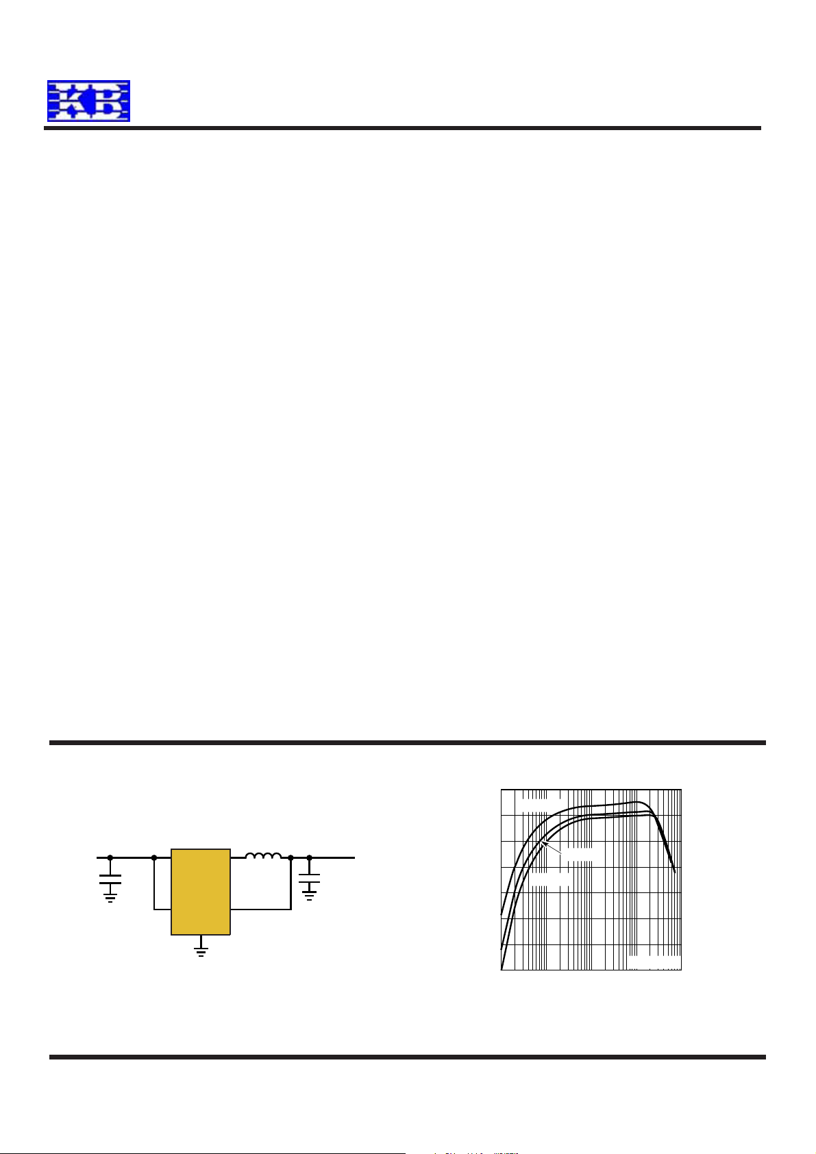
TYPICAL APPLICATION
V
3.6V
TO 6.5V
IN
+
C
IN
4.7µF
Tan
4
V
IN
KB3426-3.3
1
RUN
V
GND
2
Figure 1a. High Efficiency Step-Down Converter
SW
OUT
4.7µH
3
5
C
OUT
10µF
CER
V
OUT
3.3V
800mA
95
VIN = 3.6V
90
85
80
75
EFFICIENCY (%)
70
65
60
0.1 10 100 1000
VIN = 3.8V
VIN = 4.2V
1
OUTPUT CURRENT (mA)
V
OUT
Figure 1b. Efficiency vs Load Current
= 3.3V
1
Page 2
Kingbor Technology Co.,Ltd
TEL:(86)0755-26508846 FAX:(86)0755-26509052
KB3426
ABSOLUTE MAXIMUM RATINGS
(Note 1)
Input Supply Voltage .................................. –0.3V to 6.5V
RUN, VFB Voltages ..................................... – 0.3V to V
IN
SW Voltage .................................. –0.3V to (VIN + 0.3V)
P-Channel Switch Source Current (DC) ............. 800mA
N-Channel Switch Sink Current (DC) ................. 800mA
PACkAGE/ORDER INFORMATION
ORDER PART
TOP VIEW
Marking
RUN 1
GND 2
SW 3
S5 PACKAGE
5-LEAD PLASTIC SOT-23
T
= 125°C, eJA = 250°C/ W, eJC = 90°C/ W
JMAX
5 V
4 V
FB
IN
NUMBER
KB3426-ADJ
Top Marking
A17x
A16x
x: date code
Peak SW Sink and Source Current ........................ 1.3A
Operating Temperature Range (Note 2) .. – 40°C to 85°C
Junction Temperature (Note 3)............................ 125°C
Storage Temperature Range ................ –65°C to 150°C
Lead Temperature (Soldering, 10 sec)................. 300°C
ORDER PART
TOP VIEW
Marking
RUN 1
GND 2
SW 3
S5 PACKAGE
5-LEAD PLASTIC SOT-23
T
= 125°C, eJA = 250°C/ W, eJC = 90°C/ W
JMAX
5 V
4 V
OUT
IN
NUMBER
KB3426B-3.3
Top Marking
A33x
KB3426B-1.8
Top Marking
A37x
x: date code
ELECTRICAL CHARACTERISTICS
The● denotes specifications which apply over the full operating temperature range, otherwise specifications are TA = 25°C.
VIN = 3.6V unless otherwise specified.
SYMBOL PARAMETER CONDITIONS MIN TYP MAX UNITS
I
VFB
V
FB
6V
FB
V
OUT
6V
OUT
I
PK
V
LOADREG
V
IN
I
S
f
OSC
R
PFET
R
NFET
I
LSW
Feedback Current ● ±30 nA
Regulated Feedback Voltage KB3426 (Note 4) TA = 25°C 0.5880 0.6 0.6120 V
KB3426 (Note 4) 0 °C T
KB3426 (Note 4) –40 °C ) T
Reference Voltage Line Regulation VIN = 2.5V to 5.5V (Note 4) ● 0.04 0.4 %/V
Regulated Output Voltage KB3426-1.8, I
KB3426-3.3, I
Output Voltage Line Regulation VIN = 2.5V to 5.5V ● 0.04 0.4 %/V
Peak Inductor Current VIN = 3V, VFB = 0.5V or V
Duty Cycle < 35%
Output Voltage Load Regulation 0.5 %
Input Voltage Range ● 2.5 6.5 V
Input DC Bias Current (Note 5)
Active Mode V
Sleep Mode V
Shutdown V
Oscillator Frequency VFB = 0.6V or V
R
of P-Channel FET ISW = 100mA 0.4 0.5 1
DS(ON)
R
of N-Channel FET ISW = –100mA 0.35 0.45 1
DS(ON)
SW Leakage V
= 0.5V or V
FB
= 0.62V or V
FB
= 0V, VIN = 4.2V 0.1 1 µA
RUN
= 0V or V
V
FB
= 0V, VSW = 0V or 5V, VIN = 5V ±0.01 ±1 µA
RUN
OUT
OUT
OUT
OUT
OUT
OUT
) 85°C 0.5865 0.6 0.6135 V
A
) 85°C ● 0.5850 0.6 0.6150 V
A
= 100mA ● 1.746 1.800 1.854 V
= 100mA ● 3.234 3.300 3.366 V
= 90%, 0.75 1 1.25 A
OUT
= 90%, I
= 103%, I
= 100% ● 1.2 1.5 1.8 MHz
= 0V 210 kHz
= 0A 300 400 µA
LOAD
= 0A 20 35 µA
LOAD
2
Page 3
Kingbor Technology Co.,Ltd
TEL:(86)0755-26508846 FAX:(86)0755-26509052
KB3426
ELECTRICAL CHARACTERISTICS
The ● denotes specifications which apply over the full operating temperature range, otherwise specifications are TA = 25°C.
= 3.6V unless otherwise specified.
V
IN
SYMBOL PARAMETER CONDITIONS MIN TYP MAX UNITS
V
I
RUN
RUN
RUN Threshold
RUN Leakage Current ● ±0.01 ±1 µA
●
0.3 1 1.5 V
Note 1: Absolute Maximum Ratings are those values beyond which the life
of a device may be impaired.
Note 2: The KB3426E is guaranteed to meet performance specifications
from 0°C to 70°C. Specifications over the –40°C to 85°C operating
temperature range are assured by design, characterization and correlation
with statistical process controls.
Note 3: T
dissipation P
Note 4: The KB3426 is tested in a proprietary test mode that connects
V
Note 5: Dynamic supply current is higher due to the gate charge being
is calculated from the ambient temperature TA and power
J
according to the following formula:
D
KB3426: T
to the output of the error amplifier.
FB
delivered at the switching frequency.
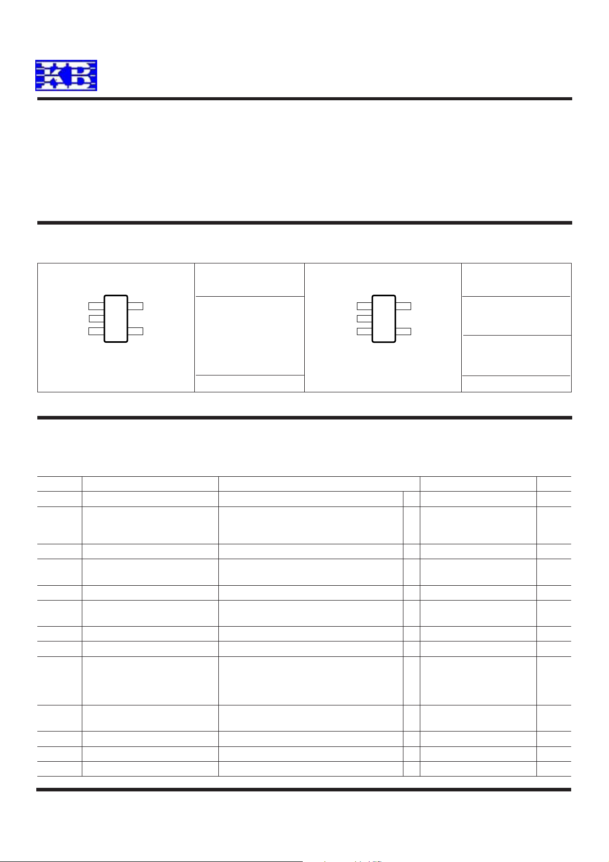
TYPICAL PERFORMANCE CHARACTERISTICS
(From Figure1a Except for the Resistive Divider Resistor Values)
Efficiency vs Input Voltage
100
I
95
90
85
80
75
70
EFFICIENCY (%)
65
60
55
50
= 100mA
OUT
I
= 1mA
OUT
I
= 650mA
OUT
I
= 0.1mA
OUT
V
= 1.8V
OUT
2
3
4
INPUT VOLTAGE (V)
I
OUT
= 10mA
5
6
Efficiency vs Output Current
95
V
= 1.2V
OUT
90
85
80
75
EFFICIENCY (%)
70
65
60
0.1 10 100 1000
VIN = 2.7V
VIN = 4.2V
VIN = 3.6V
1
OUTPUT CURRENT (mA)
= TA + (PD)(250°C/W)
J
Efficiency vs Output Current
95
V
90
85
80
75
EFFICIENCY (%)
70
65
60
0.1 10 100 1000
= 1.5V
OUT
VIN = 2.7V
VIN = 4.2V
VIN = 3.6V
1
OUTPUT CURRENT (mA)
Efficiency vs Output Current
100
V
= 2.5V
OUT
95
VIN = 2.7V
90
85
80
75
EFFICIENCY (%)
70
65
60
0.1 10 100 1000
VIN = 3.6V
VIN = 4.2V
1
OUTPUT CURRENT (mA)
Reference Voltage vs
Temperature
0.614
VIN = 3.6V
0.609
0.604
0.599
0.594
REFERENCE VOLTAGE (V)
0.589
0.584
–50
–25 0
TEMPERATURE (°C)
50 100 125
25 75
Oscillator Frequency vs
Temperature
1.70
VIN = 3.6V
1.65
1.60
1.55
1.50
1.45
FREQUENCY (MHz)
1.40
1.35
1.30
–50
–25 0
TEMPERATURE (°C)
50 100 125
25 75
3
Page 4
Kingbor Technology Co.,Ltd
TEL:(86)0755-26508846 FAX:(86)0755-26509052
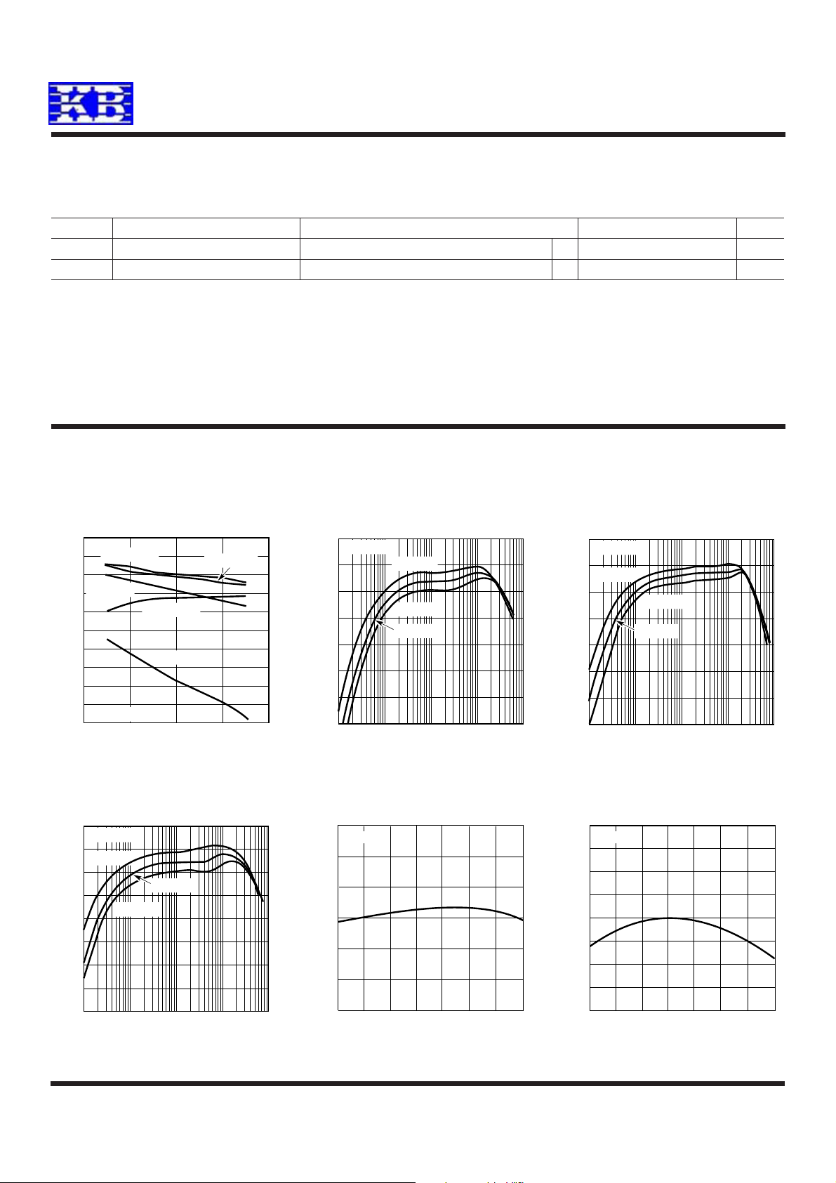
TYPICAL PERFORMANCE CHARACTERISTICS
(From Figure1a Except for the Resistive Divider Resistor Values)
KB3426
Oscillator Frequency vs
Supply Voltage
1.8
1.7
1.6
1.5
1.4
OSCILLATOR FREQUENCY (MHz)
1.3
1.2
0.7
0.6
0.5
0.4
(1)
0.3
DS(ON)
R
0.2
0.1
0
2
R
–50
34 56
SUPPLY VOLTAGE (V)
vs Temperature Supply Current vs Supply Voltage Supply Current vs Temperature
DS(ON)
VIN = 4.2V
MAIN SWITCH
SYNCHRONOUS SWITCH
–25 0
VIN = 3.6V
25 75
TEMPERATURE (°C)
VIN = 2.7V
50 100 125
Output Voltage vs Load Current
1.844
VIN = 3.6V
1.834
1.824
1.814
1.804
1.794
OUTPUT VOLTAGE (V)
1.784
1.774
100 900
0
200 300 400 500 600 700 800
LOAD CURRENT (mA)
50
V
= 1.8V
OUT
45
40
35
30
25
20
15
SUPPLY CURRENT (µA)
10
= 0A
I
LOAD
5
0
2
3
4
SUPPLY VOLTAGE (V)
R
) vs Input Voltage
DS(ON
0.7
0.6
0.5
0.4
(1)
0.3
DS(ON)
R
0.2
0.1
0
10
23
50
VIN = 3.6V
45
= 1.8V
V
OUT
= 0A
I
LOAD
40
35
30
25
20
15
SUPPLY CURRENT (µA)
10
5
0
5
6
–50
–25
0
MAIN
SWITCH
SYNCHRONOUS
SWITCH
46
INPUT VOLTAGE (V)
50
25
TEMPERATURE (°C)
57
100
125
75
Switch Leakage vs Temperature
300
VIN = 5.5V
RUN = 0V
250
200
150
100
SWITCH LEAKAGE (nA)
50
SYNCHRONOUS SWITCH
0
–50
–25 0
TEMPERATURE (°C)
MAIN SWITCH
50 100 125
25 75
4
Switch Leakage vs Input Voltage
120
RUN = 0V
100
80
60
40
SWITCH LEAKAGE (pA)
20
0
0
SYNCHRONOUS
234
1
INPUT VOLTAGE (V)
SWITCH
MAIN
SWITCH
56
SW
5V/DIV
V
OUT
100mV/DIV
AC COUPLED
200mA/DIV
Burst Mode Operation
I
L
V
I
LOAD
OUT
= 1.8V
= 50mA
4µs/DIVVIN = 3.6V
Page 5
Kingbor Technology Co.,Ltd
TEL:(86)0755-26508846 FAX:(86)0755-26509052
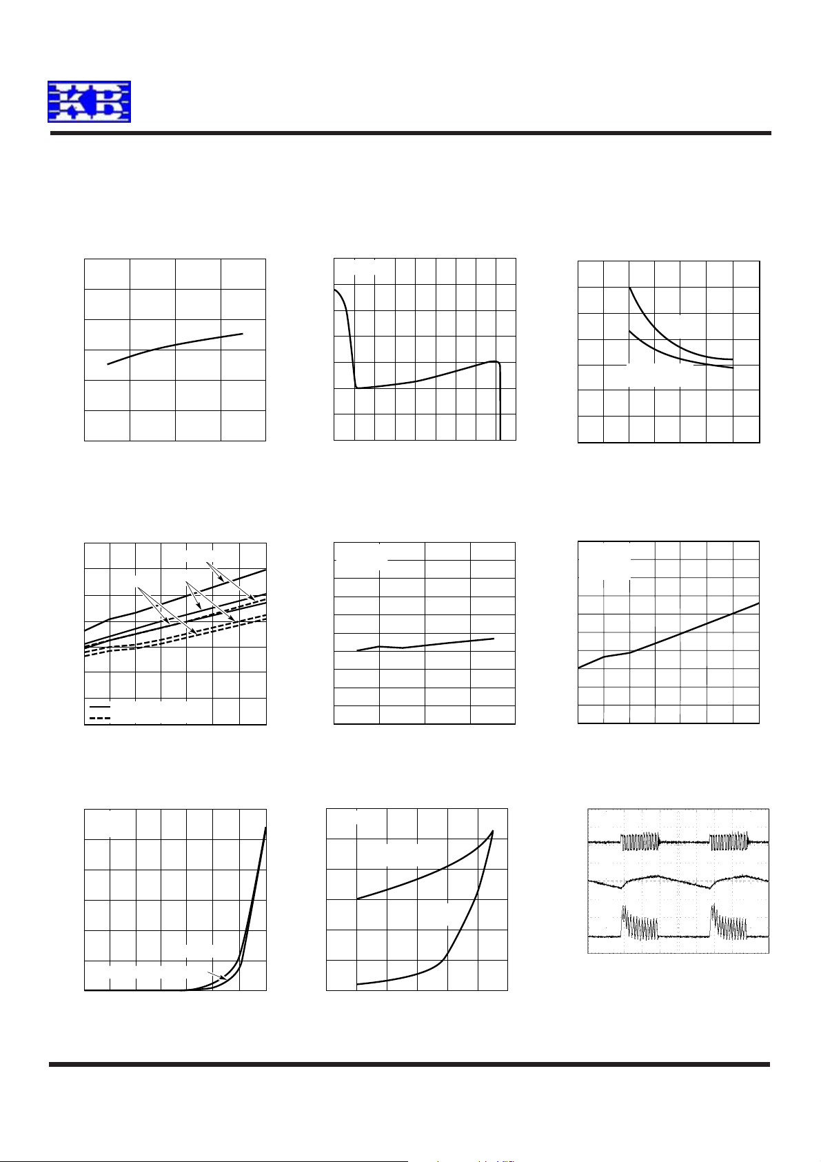
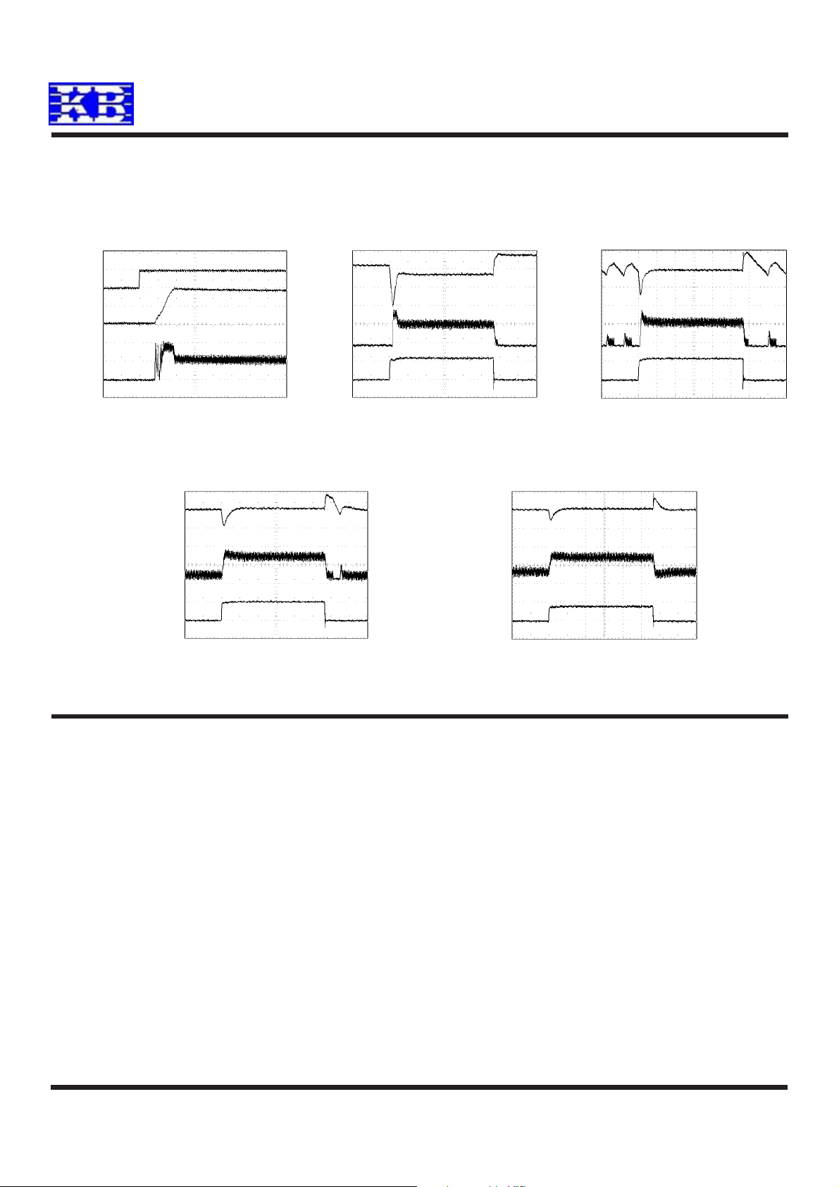
TYPICAL PERFORMANCE CHARACTERISTICS
(From Figure 1a Except for the Resistive Divider Resistor Values)
KB3426
RUN
2V/DIV
V
OUT
2V/DIV
I
LOAD
500mA/DIV
Start-Up from Shutdown
IN
V
OUT
I
LOAD
= 3.6V
= 1.8V
= 800mA
40µs/DIVV
Load Step
V
OUT
100mV/DIV
AC COUPLED
I
L
500mA/DIV
I
LOAD
500mA/DIV
V
OUT
100mV/DIV
AC COUPLED
500mA/DIV
I
LOAD
500mA/DIV
Load Step
I
L
= 3.6V
IN
V
OUT
I
LOAD
= 1.8V
= 0mA TO 800mA
20µs/DIVV
V
OUT
100mV/DIV
AC COUPLED
500mA/DIV
I
LOAD
500mA/DIV
Load Step
I
L
V
OUT
100mV/DIV
AC COUPLED
500mA/DIV
I
LOAD
500mA/DIV
Load Step
I
L
= 3.6V
IN
= 1.8V
V
OUT
I
LOAD
20µs/DIVV
= 50mA TO 800mA
= 3.6V
IN
V
= 1.8V
OUT
= 100mA TO 800mA
I
LOAD
20µs/DIVV
PIN FUNCTIONS
RUN (Pin 1): Run Control Input. Forcing this pin above
1.5V enables the part. Forcing this pin below 0.3V shuts
down the device. In shutdown, all functions are disabled
drawing <1µA supply current. Do not leave RUN floating.
GND (Pin 2): Ground Pin.
SW (Pin 3): Switch Node Connection to Inductor. This pin
connects to the drains of the internal main and synchronous power MOSFET switches.
= 3.6V
IN
= 1.8V
V
OUT
= 200mA TO 800mA
I
LOAD
20µs/DIVV
VIN (Pin 4): Main Supply Pin. Must be closely decoupled
to GND, Pin 2, with a 2.2µF or greater ceramic capacitor.
VFB (Pin 5) (kB3426): Feedback Pin. Receives the feedback voltage from an external resistive divider across the
output.
V
(Pin 5) (kB3426-1.8/kB3426-3.3): Output Volt-
OUT
age Feedback Pin. An internal resistive divider divides the
output voltage down for comparison to the internal reference voltage.
5
Page 6
Kingbor Technology Co.,Ltd
TEL:(86)0755-26508846 FAX:(86)0755-26509052
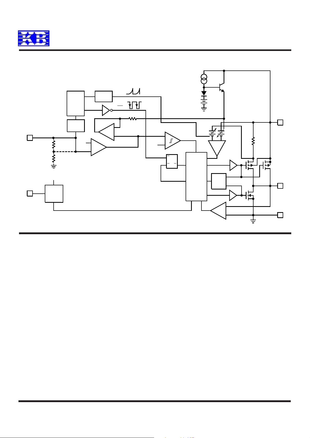
SIMPLIFIED BLOC DIAGRAM
SLOPE
COMP
OSC
–
+
EA
–
+
VFB/V
RUN
OSC
FREQ
OUT
5
V
IN
1
0.6V REF
SHIFT
R1
R2
0.6V
FB
0.4V
–
+
S
R
RS LATCH
BURST
Q
Q
SLEEP
SWITCHING
LOGIC
AND
BLANKING
CIRCUIT
0.65V
I
SHOOT-
–
COMP
ANTI-
THRU
KB3426
V
4
IN
+
51
SW
3
SHUTDOWN
OPERATION
(Refer to Functional Diagram)
Main Control Loop
The KB3426 uses a constant frequency, current mode
step-down architecture. Both the main (P-channel
MOSFET) and synchronous (N-channel MOSFET) switches
are internal. During normal operation, the internal top
power MOSFET is turned on each cycle when the oscillator
sets the RS latch, and turned off when the current comparator, I
current at which I
, resets the RS latch. The peak inductor
COMP
resets the RS latch, is controlled by
COMP
the output of error amplifier EA. When the load current
increases, it causes a slight decrease in the feedback
voltage, FB, relative to the 0.6V reference, which in turn,
causes the EA amplifier’s output voltage to increase until
the average inductor current matches the new load current. While the top MOSFET is off, the bottom MOSFET is
turned on until either the inductor current starts to reverse,
as indicated by the current reversal comparator I
RCMP
, or
the beginning of the next clock cycle.
+
I
RCMP
–
GND
2
Burst Mode Operation
The KB3426 is capable of Burst Mode operation in which
the internal power MOSFETs operate intermittently based
on load demand.
In Burst Mode operation, the peak current of the inductor
is set to approximately 200mA regardless of the output
load. Each burst event can last from a few cycles at light
loads to almost continuously cycling with short sleep
intervals at moderate loads. In between these burst events,
the power MOSFETs and any unneeded circuitry are turned
off, reducing the quiescent current to 20µA. In this sleep
state, the load current is being supplied solely from the
output capacitor. As the output voltage droops, the EA
amplifier’s output rises above the sleep threshold signaling the BURST comparator to trip and turn the top MOSFET
on. This process repeats at a rate that is dependent on the
load demand.
6
Page 7

Kingbor Technology Co.,Ltd
TEL:(86)0755-26508846 FAX:(86)0755-26509052
KB3426
OPERATION
(Refer to Functional Diagram)
Short-Circuit Protection
When the output is shorted to ground, the frequency of the
oscillator is reduced to about 210kHz, 1/7 the nominal
frequency. This frequency foldback ensures that the inductor current has more time to decay, thereby preventing
runaway. The oscillator’s frequency will progressively
increase to 1.5MHz when V
FB
or V
rises above 0V.
OUT
Dropout Operation
As the input supply voltage decreases to a value approaching the output voltage, the duty cycle increases toward the
maximum on-time. Further reduction of the supply voltage
forces the main switch to remain on for more than one cycle
until it reaches 100% duty cycle. The output voltage will then
be determined by the input voltage minus the voltage drop
across the P-channel MOSFET and the inductor.
An important detail to remember is that at low input supply
voltages, the R
of the P-channel switch increases
DS(ON)
(see Typical Performance Characteristics). Therefore, the
user should calculate the power dissipation when the
KB3426 is used at 100% duty cycle with low input voltage
(See Thermal Considerations in the Applications Information section).
in the maximum output current as a function of input
voltage for various output voltages.
Slope Compensation and Inductor Peak Current
Slope compensation provides stability in constant frequency architectures by preventing subharmonic oscillations at high duty cycles. It is accomplished internally by
adding a compensating ramp to the inductor current
signal at duty cycles in excess of 40%. Normally, this
results in a reduction of maximum inductor peak current
for duty cycles >40%. However, the KB3426 uses a
patent-pending scheme that counteracts this compensating ramp, which allows the maximum inductor peak
current to remain unaffected throughout all duty cycles.
1200
1000
V
= 1.8V
OUT
800
V
= 1.5V
OUT
600
400
200
MAXIMUM OUTPUT CURRENT (mA)
V
= 2.5V
OUT
Low Supply Operation
The KB3426 will operate with input supply voltages as
low as 2.5V, but the maximum allowable output current is
reduced at this low voltage. Figure 2 shows the reduction
0
2.5
Figure 2. Maximum Output Current vs Input Voltage
3.5 4.0 4.5
3.0
SUPPLY VOLTAGE (V)
5.0 5.5
7
Page 8

Kingbor Technology Co.,Ltd
TEL:(86)0755-26508846 FAX:(86)0755-26509052
APPLICATIONS INFORMATION
KB3426
The basic KB3426 application circuit is shown in Figure 1.
External component selection is driven by the load requirement and begins with the selection of L followed by C
C
.
OUT
IN
and
Inductor Selection
For most applications, the value of the inductor will fall in
the range of 1µH to 4.7µH. Its value is chosen based on the
desired ripple current. Large value inductors lower ripple
current and small value inductors result in higher ripple
currents. Higher VIN or V
also increases the ripple
OUT
current as shown in equation 1. A reasonable starting point
for setting ripple current is 6IL = 240mA (40% of 800mA).
6 =
I
1
L OUT
fL
()( )
£
1
V
<
²
¤
V
OUT
V
IN
¥
´
¦
(1)
The DC current rating of the inductor should be at least
equal to the maximum load current plus half the ripple
current to prevent core saturation. Thus, a 820mA rated
inductor should be enough for most applications (700mA
+ 120mA). For better efficiency, choose a low DC-resistance inductor.
The inductor value also has an effect on Burst Mode
operation. The transition to low current operation begins
when the inductor current peaks fall to approximately
200mA. Lower inductor values (higher 6IL) will cause this
to occur at lower load currents, which can cause a dip in
efficiency in the upper range of low current operation. In
Burst Mode operation, lower inductance values will cause
the burst frequency to increase.
Inductor Core Selection
Different core materials and shapes will change the size/
current and price/current relationship of an inductor.
Toroid or shielded pot cores in ferrite or permalloy materials are small and don’t radiate much energy, but generally cost more than powdered iron core inductors with
similar electrical characteristics. The choice of which style
inductor to use often depends more on the price vs size
requirements and any radiated field/EMI requirements
than on what the KB3426 requires to operate. Table 1
shows some typical surface mount inductors that work
well in KB3426 applications.
Table 1. Representative Surface Mount Inductors
PART VALUE DCR MAX DC SIZE
NUMBER (µH) (1 MAX) CURRENT (A) W × L × H (mm
Sumida 1.5 0.043 1.55 3.8 × 3.8 × 1.8
CDRH3D16 2.2 0.075 1.20
3.3 0.110 1.10
4.7 0.162 0.90
Sumida 2.2 0.116 0.950 3.5 × 4.3 × 0.8
CMD4D06 3.3 0.174 0.770
4.7 0.216 0.750
Panasonic 3.3 0.17 1.00 4.5 × 5.4 × 1.2
ELT5KT 4.7 0.20 0.95
Murata 1.0 0.060 1.00 2.5 × 3.2 × 2.0
LQH32CN 2.2 0.097 0.79
4.7 0.150 0.65
C
IN
and C
Selection
OUT
3
)
In continuous mode, the source current of the top MOSFET
is a square wave of duty cycle V
OUT/VIN
. To prevent large
voltage transients, a low ESR input capacitor sized for the
maximum RMS current must be used. The maximum
RMS capacitor current is given by:
OUT
12/
, where
VVV
[]
CI
required I
IN OMAX
RMS
OUT IN OUT
<
()
V
IN
This formula has a maximum at VIN = 2V
I
RMS
= I
/2. This simple worst-case condition is com-
OUT
monly used for design because even significant deviations
do not offer much relief. Note that the capacitor
manufacturer’s ripple current ratings are often based on
2000 hours of life. This makes it advisable to further derate
the capacitor, or choose a capacitor rated at a higher
temperature than required. Always consult the manufacturer if there is any question.
8
Page 9

Kingbor Technology Co.,Ltd
TEL:(86)0755-26508846 FAX:(86)0755-26509052
APPLICATIONS INFORMATION
KB3426
The selection of C
is driven by the required effective
OUT
series resistance (ESR).
Typically, once the ESR requirement for C
OUT
has been
met, the RMS current rating generally far exceeds the
I
RIPPLE(P-P)
requirement. The output ripple 6V
is deter-
OUT
mined by:
66 +
V I ESR
OUT L
£
²
¤
8
where f = operating frequency, C
fC
1
OUT
¥
´
¦
= output capacitance
OUT
and 6IL = ripple current in the inductor. For a fixed output
voltage, the output ripple is highest at maximum input
voltage since 6IL increases with input voltage.
Aluminum electrolytic and dry tantalum capacitors are
both available in surface mount configurations. In the case
of tantalum, it is critical that the capacitors are surge tested
for use in switching power supplies. An excellent choice is
the AVX TPS series of surface mount tantalum. These are
specially constructed and tested for low ESR so they give
the lowest ESR for a given volume. Other capacitor types
include Sanyo POSCAP, Kemet T510 and T495 series, and
Sprague 593D and 595D series. Consult the manufacturer
for other specific recommendations.
Using Ceramic Input and Output Capacitors
induce ringing at the input, V
. At best, this ringing can
IN
couple to the output and be mistaken as loop instability. At
worst, a sudden inrush of current through the long wires
can potentially cause a voltage spike at VIN, large enough
to damage the part.
When choosing the input and output ceramic capacitors,
choose the X5R or X7R dielectric formulations. These
dielectrics have the best temperature and voltage characteristics of all the ceramics for a given value and size.
Output Voltage Programming (kB3426 Only)
In the adjustable version, the output voltage is set by a
resistive divider according to the following formula:
R
2
VV
=+
OUT
£
06 1
.
²
¤
¥
´
¦
R
1
(2)
The external resistive divider is connected to the output,
allowing remote voltage sensing as shown in Figure 3.
KB3426
V
GND
0.6V ) V
FB
OUT
) 5.5V
R2
R1
Higher values, lower cost ceramic capacitors are now
becoming available in smaller case sizes. Their high ripple
current, high voltage rating and low ESR make them ideal
for switching regulator applications. Because the
KB3426’s control loop does not depend on the output
capacitor’s ESR for stable operation, ceramic capacitors
can be used freely to achieve very low output ripple and
small circuit size.
However, care must be taken when ceramic capacitors are
used at the input and the output. When a ceramic capacitor
is used at the input and the power is supplied by a wall
adapter through long wires, a load step at the output can
Figure 3. Setting the kB3426 Output Voltage
Efficiency Considerations
The efficiency of a switching regulator is equal to the
output power divided by the input power times 100%. It is
often useful to analyze individual losses to determine what
is limiting the efficiency and which change would produce
the most improvement. Efficiency can be expressed as:
Efficiency = 100% – (L1 + L2 + L3 + ...)
where L1, L2, etc. are the individual losses as a percentage
of input power.
9
Page 10

Kingbor Technology Co.,Ltd
TEL:(86)0755-26508846 FAX:(86)0755-26509052
APPLICATIONS INFORMATION
Although all dissipative elements in the circuit produce
losses, two main sources usually account for most of the
losses in KB3426 circuits: V
losses. The VIN quiescent current loss dominates the
efficiency loss at very low load currents whereas the I2R
loss dominates the efficiency loss at medium to high load
currents. In a typical efficiency plot, the efficiency curve at
very low load currents can be misleading since the actual
power lost is of no consequence as illustrated in Figure 4.
quiescent current and I2R
IN
KB3426
2
2. I
R losses are calculated from the resistances of the
internal switches, R
continuous mode, the average output current flowing
through inductor L is “chopped” between the main
switch and the synchronous switch. Thus, the series
resistance looking into the SW pin is a function of both
top and bottom MOSFET R
(DC) as follows:
RSW= (R
DS(ON)TOP
, and external inductor RL. In
SW
and the duty cycle
DS(ON)
)(DC) + (R
DS(ON)BOT
)(1 – DC)
1
0.1
0.01
0.001
POWER LOSS (W)
0.0001
0.00001
V
= 1.2V
OUT
= 1.5V
V
OUT
= 1.8V
V
OUT
= 2.5V
V
OUT
0.1 1
Figure 4. Power Lost vs Load Current
10 100 1000
LOAD CURRENT (mA)
1. The VIN quiescent current is due to two components:
the DC bias current as given in the electrical characteristics and the internal main switch and synchronous
switch gate charge currents. The gate charge current
results from switching the gate capacitance of the
internal power MOSFET switches. Each time the gate is
switched from high to low to high again, a packet of
charge, dQ, moves from VIN to ground. The resulting
dQ/dt is the current out of VINthat is typically larger than
the DC bias current. In continuous mode, I
GATECHG
=
f(QT+ QB) where QT and QB are the gate charges of the
internal top and bottom switches. Both the DC bias and
gate charge losses are proportional to VIN and thus
their effects will be more pronounced at higher supply
voltages.
The R
for both the top and bottom MOSFETs can
DS(ON)
be obtained from the Typical Performance Charateristics
curves. Thus, to obtain I2R losses, simply add RSW to
RL and multiply the result by the square of the average
output current.
Other losses including CIN and C
ESR dissipative
OUT
losses and inductor core losses generally account for less
than 2% total additional loss.
Thermal Considerations
In most applications the KB3426 does not dissipate
much heat due to its high efficiency. But, in applications
where the KB3426 is running at high ambient temperature with low supply voltage and high duty cycles, such
as in dropout, the heat dissipated may exceed the maximum junction temperature of the part. If the junction
temperature reaches approximately 150°C, both power
switches will be turned off and the SW node will become
high impedance.
To avoid the KB3426 from exceeding the maximum
junction temperature, the user will need to do some
thermal analysis. The goal of the thermal analysis is to
determine whether the power dissipated exceeds the
maximum junction temperature of the part. The temperature rise is given by:
TR= (PD)(eJA)
where PD is the power dissipated by the regulator and e
JA
is the thermal resistance from the junction of the die to the
ambient temperature.
10
Page 11

Kingbor Technology Co.,Ltd
TEL:(86)0755-26508846 FAX:(86)0755-26509052
APPLICATIONS INFORMATION
KB3426
The junction temperature, TJ, is given by:
= TA+ T
T
J
R
where TA is the ambient temperature.
As an example, consider the KB3426 in dropout at an
input voltage of 2.7V, a load current of 800mA and an
ambient temperature of 70°C. From the typical performance graph of switch resistance, the R
DS(ON)
of the
P-channel switch at 70°C is approximately 0.521. Therefore, power dissipated by the part is:
LOAD
2
• R
DS(ON)
= 187.2mW
PD = I
For the SOT-23 package, the eJA is 250°C/W. Thus, the
junction temperature of the regulator is:
TJ= 70°C + (0.1872)(250) = 116.8°C
which is below the maximum junction temperature of
125°C.
Note that at higher supply voltages, the junction temperature is lower due to reduced switch resistance (R
DS(ON)
).
A second, more severe transient is caused by switching in
loads with large (>1µF) supply bypass capacitors. The
discharged bypass capacitors are effectively put in parallel
with C
, causing a rapid drop in V
OUT
. No regulator can
OUT
deliver enough current to prevent this problem if the load
switch resistance is low and it is driven quickly. The only
solution is to limit the rise time of the switch drive so that
the load rise time is limited to approximately (25 • C
LOAD
).
Thus, a 10µF capacitor charging to 3.3V would require a
250µs rise time, limiting the charging current to about
130mA.
PC Board Layout Checklist
When laying out the printed circuit board, the following
checklist should be used to ensure proper operation of the
KB3426. These items are also illustrated graphically in
Figures 5 and 6. Check the following in your layout:
1. The power traces, consisting of the GND trace, the SW
trace and the VIN trace should be kept short, direct and
wide.
Checking Transient Response
The regulator loop response can be checked by looking at
the load transient response. Switching regulators take
several cycles to respond to a step in load current. When
a load step occurs, V
equal to (6I
resistance of C
discharge C
• ESR), where ESR is the effective series
LOAD
OUT
, which generates a feedback error signal.
OUT
The regulator loop then acts to return V
state value. During this recovery time V
immediately shifts by an amount
OUT
. 6I
also begins to charge or
LOAD
to its steady-
OUT
can be moni-
OUT
tored for overshoot or ringing that would indicate a stability
problem. For a detailed explanation of switching control
loop theory, see Application Note 76.
2. Does the VFB pin connect directly to the feedback
resistors? The resistive divider R1/R2 must be connected between the (+) plate of C
3. Does the (+) plate of C
connect to VIN as closely as
IN
and ground.
OUT
possible? This capacitor provides the AC current to the
internal power MOSFETs.
4. Keep the switching node, SW, away from the sensitive
VFB node.
5. Keep the (–) plates of CIN and C
as close as possible.
OUT
11
Page 12

Kingbor Technology Co.,Ltd
TEL:(86)0755-26508846 FAX:(86)0755-26509052
APPLICATIONS INFORMATION
KB3426
1
RUN
KB3426
2
–
V
C
OUT
OUT
+
L1
BOLD LINES INDICATE HIGH CURRENT PATHS
GND
3
SW
Figure 5a. kB3426 Layout Diagram
VIA TO V
PIN 1
V
OUT
SW
L1
KB3426
5
V
FB
R2
4
V
IN
C
IN
+
R1
C
FWD
–
V
OUT
+
V
IN
BOLD LINES INDICATE HIGH CURRENT PATHS
1
RUN
KB3426B-1.8
2
GND
C
OUT
3
L1
SW
5
V
OUT
4
V
IN
C
IN
+
V
IN
Figure 5b. kB3426B-1.8 Layout Diagram
VIA TO GND
R1
IN
R2
C
FWD
V
IN
VIA TO V
OUT
PIN 1
V
OUT
SW
L1
KB3426B-1.8
VIA TO V
VIA TO V
IN
OUT
V
IN
C
OUT
GND
C
IN
Figure 6a. kB3426 Suggested Layout
Design Example
As a design example, assume the KB3426 is used in a
single lithium-ion battery-powered cellular phone
application. The VIN will be operating from a maximum of
4.2V down to about 2.7V. The load current requirement
is a maximum of 0.6A but most of the time it will be in
standby mode, requiring only 2mA. Efficiency at both low
and high load currents is important. Output voltage is
2.5V. With this information we can calculate L using
equation (1),
L
1
=
fI
()6()
£
V
OUT
L
<
1
²
¤
V
OUT
V
IN
¥
´
¦
(3)
C
OUT
GND
C
IN
Figure 6b. kB3426-1.8 Suggested Layout
Substituting V
= 2.5V, VIN= 4.2V, 6IL= 240mA and
OUT
f = 1.5MHz in equation (3) gives:
V
25
L
1 5 240
.
MHz mA
.( )..
£
1
²
¤
25
42
V
¥
=µ
281
´
¦
V
H= <
.
A 2.2µH inductor works well for this application. For best
efficiency choose a 720mA or greater inductor with less
than 0.21 series resistance.
CINwill require an RMS current rating of at least 0.3A
I
LOAD(MAX)
/2 at temperature and C
will require an ESR
OUT
of less than 0.251. In most cases, a ceramic capacitor will
satisfy this requirement.
12
Page 13

Kingbor Technology Co.,Ltd
TEL:(86)0755-26508846 FAX:(86)0755-26509052
APPLICATIONS INFORMATION
KB3426
For the feedback resistors, choose R1 = 316k. R2 can
then be calculated from equation (2) to be:
R
2
V
2.7V
TO 6.5V
£
OUT
²
¤
06
IN
¥
Rk
1 1 1000= <
=
´
¦
.
4.7µH
4
V
C
IN
+
10µF
Tan
IN
KB3426
1
RUN
GND
** TAIYO YUDEN JMK316BJ106ML
3
SW
V
FB
2
22pF
5
1M
316k
C
OUT
10µF
CER
**
V
OUT
2.5V
V
Figure 7a
TYPICAL APPLICATION
Figure 7 shows the complete circuit along with its efficiency curve.
100
V
= 2.5V
OUT
95
VIN = 2.7V
90
85
80
75
EFFICIENCY (%)
70
65
60
0.1 10 100 1000
VIN = 3.6V
VIN = 4.2V
1
OUTPUT CURRENT (mA)
Figure 7b
95
V
= 1.5V
OUT
90
VIN = 2.7V
85
80
75
EFFICIENCY (%)
70
65
60
0.1 10 100 1000
VIN = 4.2V
VIN = 3.6V
1
OUTPUT CURRENT (mA)
Single Li-Ion 1.5V/800mA Regulator for
High Efficiency and Small Footprint
V
IN
2.7V
TO 6.5V
100mV/DIV
AC COUPLED
500mA/DIV
500mA/DIV
V
I
LOAD
+
OUT
C
10 µF
Tan
I
L
IN
V
I
LOAD
4
V
1
RUN
= 3.6V
IN
= 1.5V
OUT
= 0A TO 800mA
SW
IN
KB3426B-1.5
V
OUT
GND
2
20µs/DIVV
4.7µH
3
†
C
OUT1
10µF
5
†
TAIYO YUDEN JMK316BJ106ML
CER
100mV/DIV
AC COUPLED
500mA/DIV
500mA/DIV
V
1.5V
V
I
LOAD
OUT
OUT
I
L
= 3.6V
IN
= 1.5V
V
OUT
I
LOAD
20µs/DIVV
= 200mA TO 800mA
13
Page 14

Kingbor Technology Co.,Ltd
TEL:(86)0755-26508846 FAX:(86)0755-26509052
TYPICAL APPLICATION
Single Li-Ion 1.2V/800mA Regulator for High Efficiency and Small Footprint
KB3426
95
V
= 1.2V
OUT
90
85
80
75
EFFICIENCY (%)
70
65
60
0.1 10 100 1000
VIN = 2.7V
VIN = 4.2V
VIN = 3.6V
1
OUTPUT CURRENT (mA)
V
IN
2.7V
TO 6.5V
100mV/DIV
AC COUPLED
500mA/DIV
500mA/DIV
V
I
LOAD
OUT
C
+
10 µF
Tan
I
L
4
IN
1
= 1.2V
V
OUT
= 0mA TO 800mA
I
LOAD
V
IN
KB3426
RUN
GND
4.7µH
3
SW
V
FB
2
20µs/DIVVIN = 3.6V
22pF
5
300k
300k
** TAIYO YUDEN JMK316BJ106ML
V
1.2V
C
**
OUT
10µF
CER
V
OUT
100mV/DIV
AC COUPLED
500mA/DIV
I
LOAD
500mA/DIV
OUT
I
L
= 3.6V
IN
V
OUT
I
LOAD
= 1.2V
20µs/DIVV
= 200mA TO 800mA
V
IN
3.6V
to 6.5V
100
VIN = 5V
= 3.3V
V
OUT
95
90
85
80
75
EFFICIENCY (%)
70
65
60
0.1 10 100 1000
1
OUTPUT CURRENT (mA)
C
IN
+
4.7µF
Tan
Tiny 3.3V/800mA Buck Regulator
4.7µH
4
V
IN
KB3426B-3.3
1
RUN
GND
3
SW
NC
5
V
FB
2
0
NC
** TAIYO YUDEN JMK316BJ106ML
V
OUT
100mV/DIV
AC COUPLED
I
500mA/DIV
I
LOAD
500mA/DIV
C
**
OUT
10µF
CER
L
= 5V
IN
= 3.3V
V
OUT
= 200mA TO 800mA
I
LOAD
V
OUT
3.3V
800mA
20µs/DIVV
14
Page 15

Kingbor Technology Co.,Ltd
TEL:(86)0755-26508846 FAX:(86)0755-26509052
PACAGE DESCRIPTION
KB3426
SOT23-5
2.9±0.2
1.9±0.2
(0.95) (0.95)
54
123
0.4±0.1
+0.2
1.6
–0.1
2.8±0.3
1.1
0.8
+0.2
–0.1
±0.1
0.15
0 to 0.1
0.2 MIN.
+0.1
–0.05
15
Page 16

Kingbor Technology Co.,Ltd
TEL:(86)0755-26508846 FAX:(86)0755-26509052
TYPICAL APPLICATION
Single Li-Ion 1.8V/800mA Regulator for Low Output Ripple and Small Footprint
KB3426
95
V
= 1.8V
OUT
90
85
80
75
EFFICIENCY (%)
70
65
60
VIN = 4.2V
0.1 10 100 1000
VIN = 2.7V
VIN = 3.6V
1
OUTPUT CURRENT (mA)
V
IN
2.7V
TO 6.5V
100mV/DIV
AC COUPLED
500mA/DIV
500mA/DIV
V
I
LOAD
OUT
C
+
10 µF
Tan
I
L
4
IN
1
= 3.6V
IN
= 1.8V
V
OUT
= 0mA TO 800mA
I
LOAD
V
IN
KB3426-1.8
RUN
GND
40µs/DIVV
4.7µH
3
SW
5
V
OUT
2
C
OUT1
47 µF
V
OUT
1.8V
V
OUT
100mV/DIV
AC COUPLED
500mA/DIV
I
LOAD
500mA/DIV
I
L
= 3.6V
IN
= 1.8V
V
OUT
I
LOAD
40µs/DIVV
= 200mA TO 800mA
16
Page 17

 Loading...