

Page 1
TRIPLE 8-BIT ANALOG-TO-DIGITAL CONVERTER KB2516 (Preliminary)
SUMMARY
The KB2516 is a triple 8-bit analog-to-digital converter optimized for digitizing R/G/B graphics signal from PC and
workstation. Its 140MSPS encode rate capability and analog bandwidth of 500MHz supports support display
resolution of up to SXGA (1280 × 1024) class. The IC also includes a PLL (Phase Locked Loop) system that can
be locked on horizontal line frequency, and generates the ADC clock.
FEATURES
• Analog bandwidth of 500MHz
• 3 clamps for 256 programmable levels
• 3 programmable gain amplifiers
• Analog input range: 0.5Vpp to 1.0Vpp
• Triple 8-bit ADC
• Sampling rate up to 140MHz
• Fully integrated PLL to generate the ADC clock,
which can be locked to a HSYNC
ORDERING INFORMATION
Device Package Ordering Information
KB2516 144-LQFP-2020
APPLICATIONS
• Integrated PLL divider
• Programmable clock phase control (Φstep = 7.5°)
Integrated SOG separator and HSYNC input
polarity detector
• Single and double pixel width output data bus
2
• Support I
• Power down mode
• 1.25W power dissipation
C and 3-wire serial interface
• RGB high speed digitizing
• LCD desktop monitor
• Plasma display pannel panel
RELATED PRODUCTS
KS2530 FRC & SCALER
1
Page 2
KB2516 (Preliminary) TRIPLE 8-BIT ANALOG-TO-DIGITAL CONVERTER
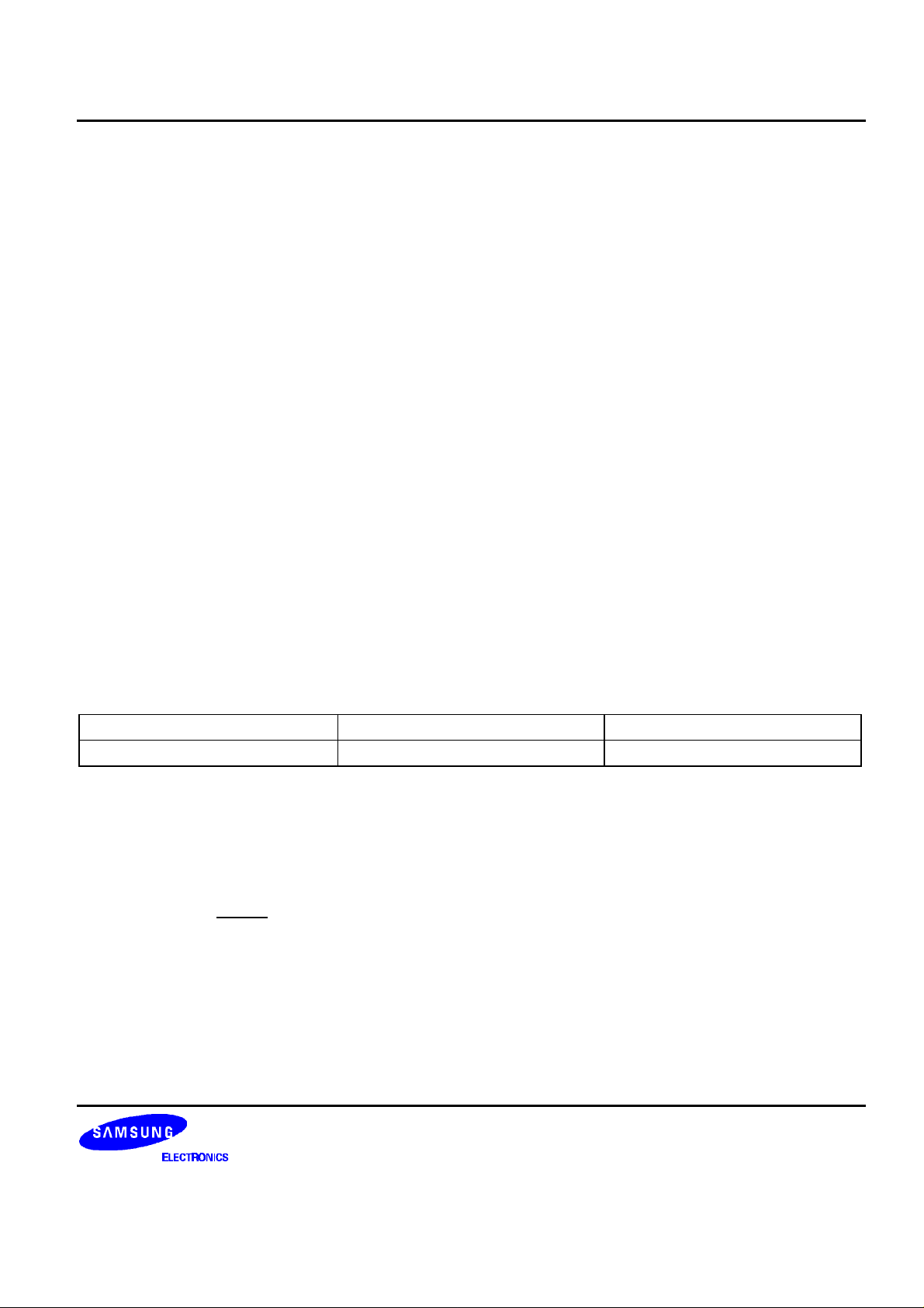
BLCOK DIAGRAM
Blue Channel
B_OUTA<7:0>
B_IN
G_IN
G_IN
Green Channel
Red Channel
CLAMP
ADC
8-bit
Output
Drver
8-bit
B_OUTB<7:0>
G_OUTA<7:0>
G_OUTB<7:0>
G_OUTA<7:0>
R_OUTB<7:0>
SDA
SCL
SEN
I2C_3W
HSYNC IN
SOG IN
VSYNC IN
CLAMP
Control
I2C and
3-wire
Sync
Processor
Gain
Control
Gain Control
CLAMP Control
PLL Control
ADC Output
Mode Control
CKA
(from PLL)
PLL
Divider
PFD
VCO
Output
Mode
CKA
Phase Shifter
HSYNC OUT
VSYNC OUT
CKA
CKB
2
Page 3
TRIPLE 8-BIT ANALOG-TO-DIGITAL CONVERTER KB2516 (Preliminary)
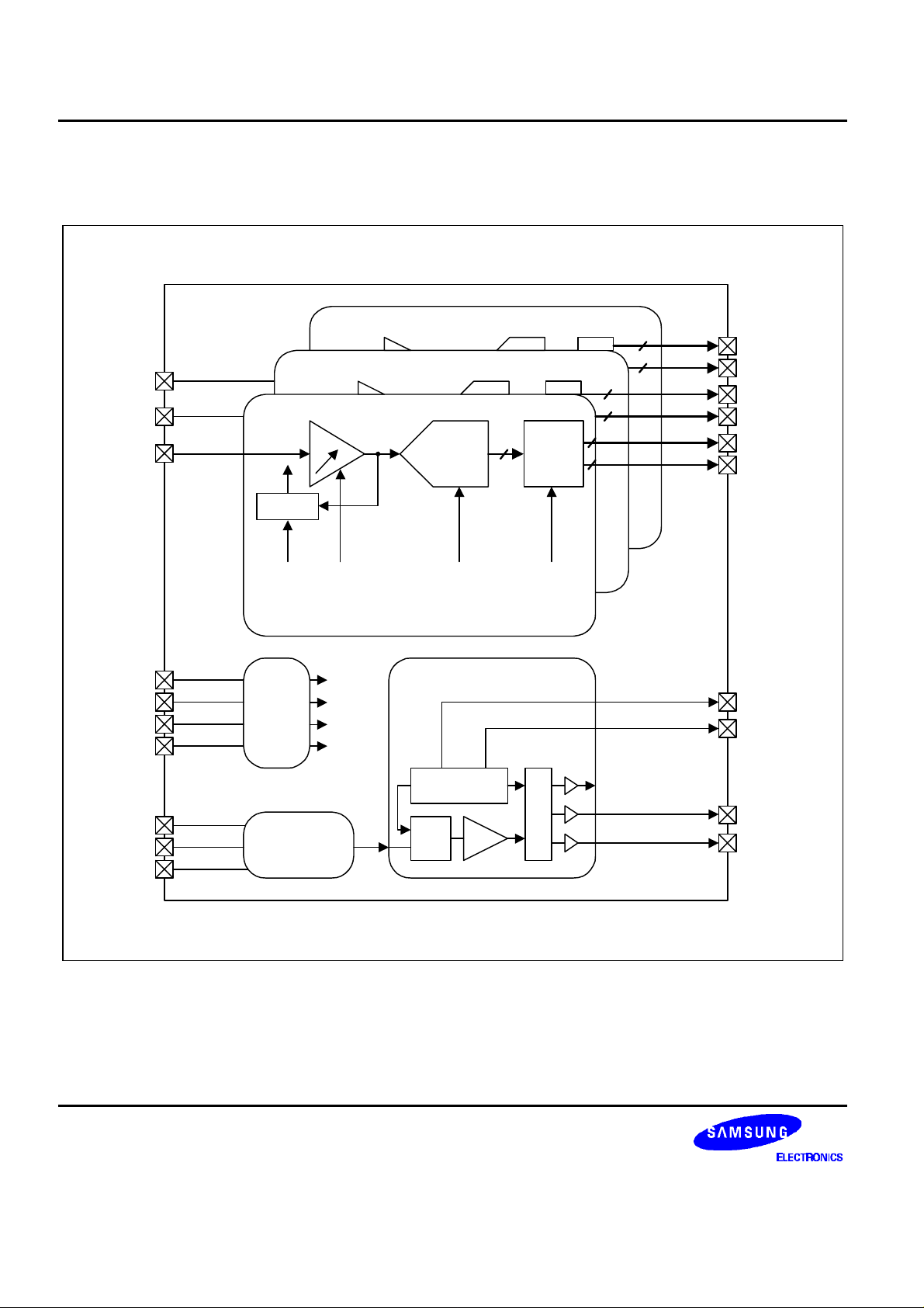
ELECTRICAL CHARACERISTICS
Symbol Parameter Conditions Min. Typ. Max. Unit
Power supply
VDDC_P Pre-amp analog supply voltage for R, G, B channels 4.75 5.0 5.25 V
VDDC_A ADC analog supply voltage for R, G, B channels 4.75 5.0 5.25 V
VDDA_A ADC analog supply voltage for R, G, B channels 3.0 3.3 3.6 V
VDDD_A ADC digital supply voltage for R, G, B channels 4.75 5.0 5.25 V
VDD_A ADC digital supply voltage for R, G, B channels 3.0 3.3 3.6 V
VDDR Output driver supply voltage for R, G, B channels 3.0 3.3 3.6 V
VDD_P PLL supply voltage 3.0 3.3 3.6 V
VDD_S Interface logic supply voltage 3.0 3.3 3.6 V
IDDC_P Pre-amp analog supply current 55 65 75 mA
IDDC_A ADC analog supply current 5V supply - 66 - mA
IDDA_A ADC analog supply current 3.3V supply - 33 - mA
IDDD_A ADC digital supply current 5V supply - 10 - mA
IDD_A ADC digital supply current 3.3V supply - 20 - mA
IDDR Output driver supply current Fclk = 140MHz, ramp input mA
IDD_P PLL supply current Fclk = 100MHz - 76 - mA
IDD_S Interface logic supply current - - mA
Ptot Total power consumption Fclk = 180MHz, ramp input - 1.25 - W
Pre-amp
f-3dB Amplifier bandwidth for R, G, B channels - 500 - MHz
VIN RGB input voltage range 0.5 0.7 1.0 Vpp
Vbs Input bias voltage for R, G, B channels 1.7 1.9 2.1 V
AVmax Voltage gain max 1.6 2.3 2.9 dB
∆AcG
∆Af1
∆Af2
tr Pre-amp rising time for R, G, B channels - 1 - nS
tf Pre-amp falling time for R, G, B channels - 1 - nS
Vbrt1
Vbrt2
Vbrt3
Coarse gain diff. between ch. for R, G, B channels -1.0 0.0 1.0 dB
Fine gain diff. 1 between ch. for R, G, B channels -1.0 0.0 1.0 dB
Fine gain diff. 2 between ch. for R, G, B channels -1.0 0.0 1.0 dB
Brightness voltage
Brightness voltage
Brightness voltage
(1)
(2)
(3)
for R, G, B channels - 1.5 - V
for R, G, B channels - 2.3 - V
for R, G, B channels - 3.0 - V
NOTES:
1. Coarse BRT = 80, Fine BRT = 00
2. Coarse BRT = 80, Fine BRT = 80
3. Coarse BRT = 80, Fine BRT = FF
3
Page 4
KB2516 (Preliminary) TRIPLE 8-BIT ANALOG-TO-DIGITAL CONVERTER
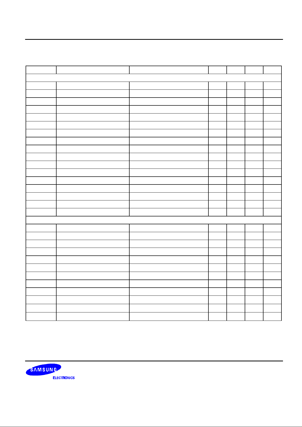
Symbol Parameter Conditions Min. Typ. Max. Unit
Sync processor
SOGdet1 SOG sync detect level 1 0.1 - - V
SOGdet2 SOG sync detect level 2 - - 1.0 V
Analog-to-digital converter
VrefT Reference top voltage 1.7 1.8 1.9 V
VrefB Reference bottom voltage 1.2 1.3 1.4 V
INL DC integral non-linearity Fclk = 75MHz, ramp input -1.0 - 1.0 LSB
DNL DC differential non-linearity Fclk = 75MHz, ramp input -0.5 - 0.5 LSB
SNDR Signal to noise & distortion
Fclk = 100MHz 36 - - dB
ratio
MAXrate Max. conversion rate 170 - - MHz
CT Cross talk Fclk = 100MHz - - -36 dB
trD Digital output rising time - - 2 nS
tfD Digital output falling time - - 2 nS
Phase-locked loop
fref PLL reference clock frequency 20 - 150 KHz
fclk Maximum clock frequency 180 MHz
DRpll PLL divider ratio 512 - 4095
fvco VCO output clock frequency 17 197 MHz
tcap PLL capture time In start-up condition - 4 - ms
trcap PLL re-capture time In lock condition - - 300 us
Φstep
j
PLL
Phase shift step
Tamb = 25°C
PLL jitter Fclk = 180MHz - 200 - ps
- 7.5 - deg
4
Page 5
TRIPLE 8-BIT ANALOG-TO-DIGITAL CONVERTER KB2516 (Preliminary)
DIGITAL SPECIFICATIONS
Characteristics Symbol Min Typ Max Unit
Logic input
High level input voltage VIH VDD - 0.5 - - V
Low level input voltage VIL - - VSS + 0.5 V
High level input current IIH - 10 - uA
Low level input current IIL - 10 - UA
Input capacitance CIN - 5 - pF
Logic output
High level output voltage VOH VDD - 0.5 - - V
Low level output voltage VOL - - VSS + 0.5 V
High level input current IOH - 100 - uA
Low level input current IOL - 100 - uA
5
Page 6
KB2516 (Preliminary) TRIPLE 8-BIT ANALOG-TO-DIGITAL CONVERTER
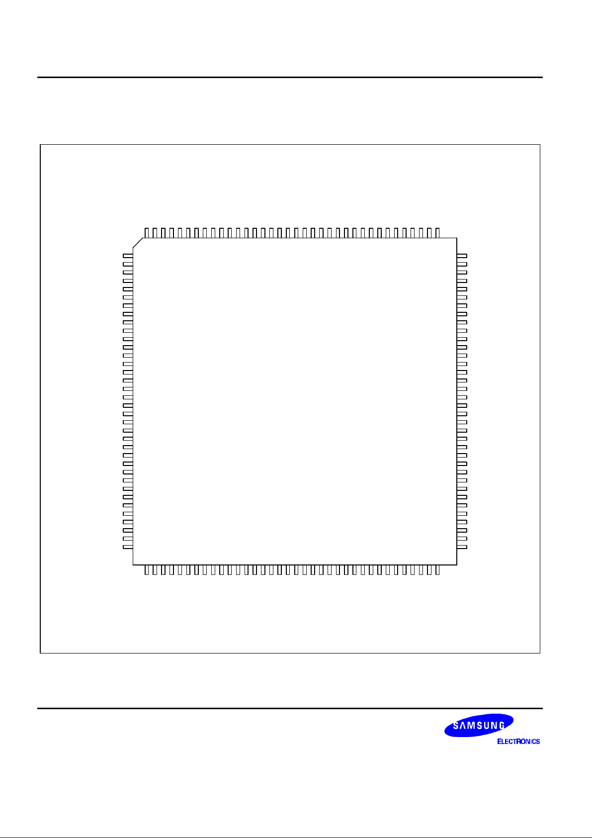
PIN ASSIGNMENT
VSSC_AR
VDDC_AR
ITEST
VDD_DAC
VSS_DAC
VBB2
VDDD_A
VSSD_A
VINP
VINN
VREFT
VREFB
VDDG
VSSG
PDB
RESETB_EX
HSYNCO
ADC_CKB
ADC_CK
VSYNCO
VDD_A
VSS_A
NC2
NC1
VSSR_RA
VDDR_RA
R_OUTA0
R_OUTA1
R_OUTA2
R_OUTA3
R_OUTA4
R_OUTA5
R_OUTA6
R_OUTA7
VSSR_RB
VDDR_RB
144
143
142
141
140
139
138
137
136
135
134
133
132
131
130
129
128
127
126
125
124
123
122
121
120
119
118
117
116
115
114
113
112
111
110
VDDA_AR
VSSA_AR
R_IN
VDDC_PR
R_VOUT1
VSSC_PR
R_CLPC
VDDC_AG
VSSC_AG
VDDA_AG
VSSA_AG
G_IN
VDDC_PG
G_VOUT1
VSSC_PG
G_CLPC
VDDC_AB
VSSC_AB
VDDA_AB
VSSA_AB
VSSA_AB
VDDC_PB
B_VOUT1
VSSC_PB
B_CLPC
VDDC_SP
VSSC_SP
CLPex
DETCAP
SOG_IN
HSYNC_IN
HSmic
SOGOUT
VDD_SI
VSS_SI
I2C_3W
1
2
3
4
5
6
7
8
9
10
11
12
13
14
15
16
17
18
19
20
21
22
23
24
25
26
27
28
29
30
31
32
33
34
35
36
3738394041424344454647484950515253545556575859606162636465666768697071
KB2516
144-TQFP-2020
109
108
107
106
105
104
103
102
101
100
72
99
98
97
96
95
94
93
92
91
90
89
88
87
86
85
84
83
82
81
80
79
78
77
76
75
74
73
R_OUTB0
R_OUTB1
R_OUTB2
R_OUTB3
R_OUTB4
R_OUTB5
R_OUTB6
R_OUTB7
VDDR_GA
VSSR_GA
G_OUTA0
G_OUTA1
G_OUTA2
G_OUTA3
G_OUTA4
G_OUTA5
G_OUTA6
G_OUTA7
G_OUTB0
G_OUTB1
G_OUTB2
G_OUTB3
G_OUTB4
G_OUTB5
G_OUTB6
G_OUTB7
VDDR_GB
VSSR_GB
B_OUTA0
B_OUTA1
B_OUTA2
B_OUTA3
B_OUTA4
B_OUTA5
B_OUTA6
B_OUTA7
SCL
SDA
ADDR_EX0
ADDR_EX1
SEN
COAST
VSS_PP
VDD_PP
VDD_PV
ADC_CKEX
VCTRL
ITEST1
VSS_PC
VDD_PC
VDD_PO
VSS_PO
VSS_PK
VSS_PD
VDD_PD
CKB
VDD_PK
CKC
VBB1
VSSR_BB
B_OUTB7
B_OUTB7
VDDR_BB
B_OUTB6
B_OUTB5
B_OUTB4
B_OUTB3
B_OUTB2
B_OUTB1
VSSR_BA
B_OUTB0
VDDR_BA
6
Page 7

TRIPLE 8-BIT ANALOG-TO-DIGITAL CONVERTER KB2516 (Preliminary)
PIN DESCRIPTION
Table 1. Pin Description
No Name Description
1 VSSC_AR Red channel ADC 0V analog power supply
2 VDDC_AR Red channel ADC 5V analog power supply
3 R_IN Red channel analog input signal
4 VDDC_PR Red channel pre-amp 5V power supply
5 R_VOUT1 Red channel pre-amp output signal
6 VSSC_PR Red channel pre-amp 0V power supply
7 R_CLPC Red channel clamp control external cap.
8 VDDA_AG Green channel ADC 3.3V analog power supply
9 VSSA_AG Green channel ADC 0V analog power supply
10 VSSC_AG Green channel ADC 0V analog power supply
11 VDDC_AG Green channel ADC 5V analog power supply
12 G_IN Green channel analog input signal
13 VDDC_PG Green channel pre-amp 5V power supply
14 G_VOUT1 Green channel pre-amp output signal
15 VSSC_PG Green channel pre-amp 0V power supply
16 G_CLPC Green channel clamp control external cap.
17 VDDA_AB Blue channel ADC 3.3V analog power supply
18 VSSA_AB Blue channel ADC 0V analog power supply
19 VSSC_AB Blue channel ADC 0V analog power supply
20 VDDC_AB Blue channel ADC 5V analog power supply
21 B_IN Blue channel analog input signal
22 VDDC_PB Blue channel pre-amp 5V power supply
23 B_VOUT1 Blue channel pre-amp output signal
24 VSSC_PB Blue channel pre-amp 0V power supply
25 B_CLPC Blue channel clamp control external cap.
26 VDDC_SP SyncProc 5V power supply
27 VSSC_SP SyncProc 0V power supply
28 CLPex External clamp signal input pin
29 DETCAP SOG polarity output
30 SOG_IN SOG signal input pin
31 HSYNC_IN HSYNC signal input pin
32 Test
7
Page 8
KB2516 (Preliminary) TRIPLE 8-BIT ANALOG-TO-DIGITAL CONVERTER
Table 1. Pin Description (Continued)
No Name Description
33 SOGOUT SOG output signal pin
34 VDD_SI Serial interface 3.3V digital power supply
35 VSS_SI Serial interface 0V digital power supply
36 I2C_3W
Serial interface mode selection between I2C and 3-wire
37 ADDR_EX0 Slave address control bit
38 ADDR_EX1 Slave address control bit
39 SDA Serial interface data signal pin
40 SCL Serial interface clock signal pin
41 SEN Signal enable for 3-wire serial interface
42 COAST COAST signal input
43 ADC_CKEX External analog to digital converter clock input
44 VDD_PP PLL 3.3V phase detector power supply
45 VSS_PP PLL 0V phase detector power supply
46 VSS_PV PLL 0V analog power supply
47 VDD_PV PLL 3.3V analog power supply
48 VCTRL VCO control voltage
49 ITEST1 Bandgap reference current test pin
50 VDD_PC PLL 3.3V charge-pump power supply
51 VSS_PC PLL 0V charge-pump power supply
52 VDD_PO PLL 3.3V VCO power supply
53 VSS_PO PLL 0V VCO power supply
54 VDD_PD PLL 3.3V digital power supply
55 VSS_PD PLL 0V digital power supply
56 VSS_PK PLL 0V clock driver power supply
57 CKB PLL output clock with ADC frequency (phase control available)
58 VDD_PK PLL 3.3V clock driver power supply
59 CKC PLL output clock with ADC frequency (phase control available)
60 VBB1 Substrate 0V power supply
61 VSSR_BB Blue channel ADC output B driver power supply (0V)
62 VDDR_BB Blue channel ADC output B driver power supply (3.3V)
63 B_OUTB7 Blue channel ADC digital output B bit 7
64 B_OUTB6 Blue channel ADC digital output B bit 6
65 B_OUTB5 Blue channel ADC digital output B bit 5
66 B_OUTB4 Blue channel ADC digital output B bit 4
67 B_OUTB3 Blue channel ADC digital output B bit 3
8
Page 9
TRIPLE 8-BIT ANALOG-TO-DIGITAL CONVERTER KB2516 (Preliminary)
Table 1. Pin Description (Continued)
No Name Description
68 B_OUTB2 Blue channel ADC digital output B bit 2
69 B_OUTB1 Blue channel ADC digital output B bit 1
70 B_OUTB0 Blue channel ADC digital output B bit 0
71 VSSR_BA Blue channel ADC output A driver power supply (0V)
72 VDDR_BA Blue channel ADC output A driver power supply (3.3V)
73 B_OUTA7 Blue channel ADC digital output A bit 7
74 B_OUTA6 Blue channel ADC digital output A bit 6
75 B_OUTA5 Blue channel ADC digital output A bit 5
76 B_OUTA4 Blue channel ADC digital output A bit 4
77 B_OUTA3 Blue channel ADC digital output A bit 3
78 B_OUTA2 Blue channel ADC digital output A bit 2
79 B_OUTA1 Blue channel ADC digital output A bit 1
80 B_OUTA0 Blue channel ADC digital output A bit 0
81 VSSR_GB Green channel ADC output B driver power supply (0V)
82 VDDR_GB Green channel ADC output B driver power supply (3.3V)
83 G_OUTB7 Green channel ADC digital output B bit 7
84 G_OUTB6 Green channel ADC digital output B bit 6
85 G_OUTB5 Green channel ADC digital output B bit 5
86 G_OUTB4 Green channel ADC digital output B bit 4
87 G_OUTB3 Green channel ADC digital output B bit 3
88 G_OUTB2 Green channel ADC digital output B bit 2
89 G_OUTB1 Green channel ADC digital output B bit 1
90 G_OUTB0 Green channel ADC digital output B bit 0
91 G_OUTA7 Green channel ADC digital output A bit 7
92 G_OUTA6 Green channel ADC digital output A bit 6
93 G_OUTA5 Green channel ADC digital output A bit 5
94 G_OUTA4 Green channel ADC digital output A bit 4
95 G_OUTA3 Green channel ADC digital output A bit 3
96 G_OUTA2 Green channel ADC digital output A bit 2
97 G_OUTA1 Green channel ADC digital output A bit 1
98 G_OUTA0 Green channel ADC digital output A bit 0
99 VSSR_GA Green channel ADC output A driver power supply (0V)
100 VDDR_GA Green channel ADC output A driver power supply (3.3V)
101 R_OUTB7 Red channel ADC digital output B bit 7
102 R_OUTB6 Red channel ADC digital output B bit 6
9
Page 10

KB2516 (Preliminary) TRIPLE 8-BIT ANALOG-TO-DIGITAL CONVERTER
Table 1. Pin Description (Continued)
No Name Description
103 R_OUTB5 Red channel ADC digital output B bit 5
104 R_OUTB4 Red channel ADC digital output B bit 4
105 R_OUTB3 Red channel ADC digital output B bit 3
106 R_OUTB2 Red channel ADC digital output B bit 2
107 R_OUTB1 Red channel ADC digital output B bit 1
108 R_OUTB0 Red channel ADC digital output B bit 0
109 VDDR_RB Red channel ADC output B driver power supply (3.3V)
110 VSSR_RB Red channel ADC output B driver power supply (0V)
111 R_OUTA7 Red channel ADC digital output A bit 7
112 R_OUTA6 Red channel ADC digital output A bit 6
113 R_OUTA5 Red channel ADC digital output A bit 5
114 R_OUTA4 Red channel ADC digital output A bit 4
115 R_OUTA3 Red channel ADC digital output A bit 3
116 R_OUTA2 Red channel ADC digital output A bit 2
117 R_OUTA1 Red channel ADC digital output A bit 1
118 R_OUTA0 Red channel ADC digital output A bit 0
119 VDDR_RA Red channel ADC output A driver power supply (3.3V)
120 VSSR_RA Red channel ADC output A driver power supply (0V)
121 NC1 No connection
122 NC2
123 VSS_A ADC 0V digital power supply
124 VDD_A ADC 3.3V digital power supply
125 VSYNCO VSYNC output
126 ADC_CK ADC clock output
127 ADC_CKB Inverted ADC clock output
128 HSYNCO HSYNC output
129 RESETB_EX External inverted reset signal input
130 PDB Power down control pin (input)
131 VSSG ADC 0V analog power supply
132 VDDG ADC 3.3V analog power supply
133 VREFB ADC reference bottom voltage
134 VREFT ADC reference top voltage
135 VINN ADC negative input for test
136 VINP ADC positive input for test
137 VSSD_A ADC 0V digital power supply
10
Page 11

TRIPLE 8-BIT ANALOG-TO-DIGITAL CONVERTER KB2516 (Preliminary)
Table 1. Pin Description (Continued)
No Name Description
138 VDDD_A ADC 5V digital power supply
139 VBB2 Substrate 0V power supply
140 VSS_DAC Pre-amp DAC 0V analog power supply
141 VDD_DAC Pre-amp DAC 5V analog power supply
142 ITEST Pre-amp control DAC current test pin
143 VDDA_AR Red channel ADC 3.3V analog power supply
144 VSSA_AR Red channel ADC 0V analog power supply
11
Page 12

KB2516 (Preliminary) TRIPLE 8-BIT ANALOG-TO-DIGITAL CONVERTER
DESCRIPTION OF EACH BLOCK
AD2516X is equipped with a pre-amp that can control the gain and clamp level and can generate the pixel clock
synchronized to input HSYNC through the internal PLL. It then converts the RGB signal from analog -to- digital
by synchronizing to the generated clock. It has a maximum conversion speed of 180MHz and is capable of
supporting up to UXGA (1600 × 1200).
VOUT1
8 bit
DAC
Gain Control
VIN
AMP1
Cex
AMP2
gm1
gm2
CLAMP
8 bit
Brightness Control
Figure 1. Pre-amp Block Diagram
DAC
VOUT (to ADC)
12
Page 13

TRIPLE 8-BIT ANALOG-TO-DIGITAL CONVERTER KB2516 (Preliminary)
Figure 1 is a block diagram of the pre-amp that is used in AD2516X. A clamp circuit is required to set the input
DC level because the RGB signal input is AC coupled as it passes through the capacitor to be sent to the preamp. The signal to control the clamp is made from the HSYNC signal in the sync processor block. The clamp
level control, which uses an 8-bit DAC, has two modes, first, the coarse level control that controls 3 RGB
channels simultaneously and, second, the fine level control that controls each channel clamp level independently.
The input signal is gain controlled through the 8-bit DAC for a maximum gain amplification of 2.3dB. As in the
clamp level control, the pre-amp has two modes: 1.) coarse level control that controls 3 RGB channels
simultaneously and 2.) fine level control which controls them independently.
VIN
T/H
15
Comps
4
OVF
UDF
8
Channel A<7:0>
Vref_tap
Gen.
8
Output Driver
Digital Correction Logic
8
Channel B<7:0>
T/H
31
Comps
5
Output Mode
Control
Figure 2. ADC Block Diagram
Figure 2 which has the 2-step pipeline configuration is a block diagram of the ADC used in AD2516X. It uses 1
overlap bit for digital correction and supports 3 output modes, signal channel mode, dual channel interleaving
mode, and dual channel parallel mode.
The sync processor block converts the HSYNC or SOG input to a positive HSYNC signal, which can be
processed by PLL, and also makes the clock signal needed for clamp level control from the HSYNC. When
HSYNC and SOG inputs enter simultaneously, it is designed to place priority on the HSYNC.
13
Page 14

KB2516 (Preliminary) TRIPLE 8-BIT ANALOG-TO-DIGITAL CONVERTER
HSYNCH
DIVCK
HSYNCH
DIVCK
VCOPFD
Divider
12 bits from
Micom
MUX
Phase
Shifter
MUX
MUX
SYNCHRO
HSYNCO, VSYNCO
Figure 3. PLL Block Diagram
0/180
0/180
0/180
CLKADC
CKB
CKC
Figure 3 is a block diagram of the PLL used in AD2516X. It generates the pixel clock by using the positive
HSYNC signal from the sync processor block and the divider coefficient determined by the resolution. The
reference clock frequency range is between 20kHz - 150kHz and the maximum output clock frequency is
180MHz. It produces two clock signals having the ADC clock frequency and each signal can have 7.5° phase
control.
AD2516X is controlled entirely through serial interface, which supports two modes -12C bus and 3-wire interface.
14
Page 15

TRIPLE 8-BIT ANALOG-TO-DIGITAL CONVERTER KB2516 (Preliminary)
REGISTER CONFIGRATION
PRE-AMP
Sub Addr. Bit Name Description Default Value
00H <7:0> S00<7:0> RGB coarse gain control 80H
01H <7:0> S01<7:0> R fine gain control 80H
02H <7:0> S02<7:0> G fine gain control 80H
03H <7:0> S03<7:0> B fine gain control 80H
04H <7:0> S04<7:0> RGB coarse bright control 80H
05H <7:0> S05<7:0> R fine bright control 80H
06H <7:0> S06<7:0> G fine bright control 80H
07H <7:0> S07<7:0> B fine bright control 80H
08H <4> PHSYNC HSYNC (input) polarity 0 00H
<3> HSEL HSYNC select 0
<2> CLPENB Clamp control 0
<1:0> CW<1:0> Clamp pulse width control 00
09H <7:0> DACTEST<7:0> DAC output selection for test FFH
ANALOG TO DIGITAL CONVERTER (ADC)
Sub Addr. Bit Name Description Default Value
0AH <7:6> M<1:0> Output mode selection 00 00H
<5> ADCK_ENB ADC clock output enable 0
<4> ADCK_INV ADC clock output inverting 0
<3> ADCK_SEL ADC clock selection control 0
<2:1> ADOM<1:0> ADC output buffer control 00
<0> 0
15
Page 16

KB2516 (Preliminary) TRIPLE 8-BIT ANALOG-TO-DIGITAL CONVERTER
PHASE LOCKED LOOP (PLL)
Sub Addr. Bit Name Description Default Value
0BH <7:6> IFRSH<1:0> VCO free running control 00 24H
<5:3> IFRSEL<2:0> VCO range control 100
<2:0> ICPSEL<2:0> Charge pump current control 100
0CH <7> VSINV VSYNC out polarity 0 00H
<6> DEINV DEN out polarity 0
<5:0> AC<5:0> CKA phase control 000000
0DH <7:6> HSYNMOD<1:0> HSYNC out polarity 00 00H
<5:0> BC<5:0> CKB phase control 000000
0EH <6> PCOAST COAST (input) polarity 0 00H
<5:0> CC<5:0> CKC phase control 000000
0FH <7:0> DIV<11:0> Divider control MSB <11:4> 01101000 68H
10H <7:4> Divider control LSB <3:0> 0000 00H
<1:0> Test <9:0> Test out length MSB <9:8> 00
11H <7:0> Test out length LSB <7:0> 00000000 00H
12H <7:0> Test <7:0> Test out delay 00000100 04H
13H <7:0> HSD<11:0> HSYNC out length MSB <11:4> 00000000 00H
14H <7:4> HSYNC out length LSB <3:0> 0100 40H
<3:0> VSL<11:0> VSYNC out length MSB <11:8> 0000
15H <7:0> VSL VSYNC out length LSB <7:0> 00000011 03H
16H <7:0> VSD<7:0> VSYNC out delay 00000000 00H
17H <7> CKA_ENB CKA output enable 0 00H
<6> CKB_ENB CKB output enable 0
16
<5> CKC_ENB CKC output enable 0
<4> CKA_INV CKA (ADC input clock) inverting 0
<3> CKB_INV CKB inverting 0
<2> CKC_INV CKC inverting 0
<1> VI_GAIN PLL VI converter gain control 0
Page 17

TRIPLE 8-BIT ANALOG-TO-DIGITAL CONVERTER KB2516 (Preliminary)
I2C AND 3-WIRE SERIAL INTERFACE BLOCK DESCRIPTION
Interface Pin:
• Input: I2C_3W, SEN, SCL, ADDR_EX<1:0>
• In-out: SDA
Pin Description:
• I2C_3W: Serial interface mode selection
0 → I2C interface mode, 1 → 3-Wire interface mode
• SEN: 3-Wire interface mode data enable signal
0 → enable, 1 → disable
• SDA: Serial data input output port
• SCL: Serial interface reference clock input
• ADDR_EX<1:0>: I2C slave address identifier
17
Page 18

KB2516 (Preliminary) TRIPLE 8-BIT ANALOG-TO-DIGITAL CONVERTER
I2C Timing Diagram
From Master to Slave From Slave to Master
- S : Start condition
- P : Stop condition
- rS: Repeated start condition
Write Mode: R/W = 0
S Slave Address ACK Sub Address ACK Sub Address ACK P
R/W
Write Mode: R/W = 0
Auto
X X A4 A3 A2 A1 A0
Auto: Sub address auto increment control bit
- 0: Disable
1: Enable
Auto = 0
S Slave Address ACK
0XXXXXXX
(sub-address)
ACK Data ACK P
0XXXXXXX
(sub-address)
ACK Data ACK0
Auto = 1
S Slave Address ACK
Data
(sub-address: N+1)
ACK
(sub-address: N+2)
1XXXXXXX
(sub-address: N)
Data
ACK
ACK P
Data
(sub-address: N)
ACK0
Auto = 1
S Slave Address ACK
Data
(sub-address: N+1)
ACK
(sub-address: N+2)
1XXXXXXX
(sub-address: N)
Data
ACK
ACK P
Data
(sub-address: N)
ACK0
18
Read Mode: R/W = 1 (Auto = X)
S Slave Address ACK Sub Address (N) ACK
Data
(sub-address: N+1)
ACK
Data
(sub-address: N+2)
ACK P
(sub-address: N+3)
Data
rS
(sub-address: N)
ACK
Data
ACKR/W
Page 19

TRIPLE 8-BIT ANALOG-TO-DIGITAL CONVERTER KB2516 (Preliminary)
Wired Interface Timing Diagram
Sub Address Format
Auto
R/W A4 A3 A2 A1 A0
Write Mode: R/W = 0
Auto: Sub address auto increment control bit
- 0: Disable
1: Enable
Auto = 0:
SEN
SCL
SDA
Sub-address (N) Data (N) Sub-address (M) Data (M)
Auto = 1: Sub-address auto increment
SEN
SCL
SDA
Sub-address (N) Data (N) Data (N+1) Data (N+2)
Figure 4. Wired Interface Write Mode Timing Diagram
19
Page 20

KB2516 (Preliminary) TRIPLE 8-BIT ANALOG-TO-DIGITAL CONVERTER
Read Mode: R/W = 1 (auto = X)
SEN
SCL
SDA
Sub-address (N) Data (N) Data (N+1) Data (N+2)
From master to slave From slave to master
Figure 5. Wired Interface Read Mode Timing Diagram
Serial Interface Description
Pre-amp Gain Control
• Coarse gain control (S00)
RGB coarse gain control with same value. (dynamic gain range: 40dB)
• Fine gain control (S01 - S03)
RGB fine gain control independently. (dynamic gain range : 11 dB)
• Coarse brightness control (S04)
RGB coarse brightness control with same value. (clamp range: 0 - 4V)
• Fine brightness control (S05 - S07)
RGB fine bright control independently. (clamp range: -0.5V - 0.5V)
Sync Processor Control
• HSYNC selection control (HSEL)
HSEL = 0: Internally polarity converted HSYNC is used
HSEL = 1: Default HSYNC is used
• HSYNC input polarity control (PHSYNC)
It is available if HSEL = 1
PHSYNC = 0: Default HSYNC input is used
PHSYNC = 1: Inverted HSYNC input is used
• Clamp control clock selection (CLPENB)
CLPENB = 0: Internal clamp signal
CLPENB = 1: External clamp signal (by CLPex)
20
Page 21

TRIPLE 8-BIT ANALOG-TO-DIGITAL CONVERTER KB2516 (Preliminary)
• Clamp pulse width control (CW)
CW<1:0> Pulse Width
00 0.31us
01 0.54us
10 0.78us
11 1.01us
• DACTEST output selection control (DACTEST)
Select one of eight DAC output current
DACTEST<7:0> Selected DAC
11111111 No selection
11111110 Coarse gain control DAC
11111101 Red channel fine gain control DAC
11111011 Green channel fine gain control DAC
11110111 Blue channel fine gain control DAC
11101111 Coarse brightness control DAC
11011111 Red channel fine brightness control DAC select
10111111 Green channel fine brightness control DAC select
01111111 Blue channel fine brightness control DAC select
Analog-to-Digital Converter (ADC) Control
• Output mode selection (M)
M<1:0> Output mode
00 Single channel output mode
01 Dual channel interleaving output mode
10 Dual channel parallel output mode
21
Page 22

KB2516 (Preliminary) TRIPLE 8-BIT ANALOG-TO-DIGITAL CONVERTER
Output mode
Single channel output mode
Dual channel interleaving output mode
Dual channel parallel output mode
• ADC clock output control (ADCK_ENB)
ADCK_ENB = 0: Output clock is enabled
ADCK_ENB = 1: Output clock is disabled (HZ)
• ADC clock output inverting control (ADCK_INV)
ADCK_INV = 0: Default ADC_CK and ADC_CKB output
ADCK_INV = 1: Inverted ADC_CK and ADC_CKB output
ADC_CK
D0 D1 D2 D3 D4 D5Channel A
Channel B HZ
Channel A
Channel B
Channel A
Channel B
D0 D2 D4
D1 D3 D5
D0 D2 D4
D1 D3 D5
• ADC clock selection control (ADCK_SEL)
ADCK_SEL = 0: Internal PLL output is used
ADCK_SEL = 1: External clock (ADC_CKEX) is used
• ADC output buffer state control (ADOM)
ADOM<1:0> Output Buffer State
00 Normal output mode
01 01010101
10 10101010
11 High impedance
Phase-Locked loop (PLL) Control
• VCO free running frequency control (IFRSH)
IFRSH<1:0> Free Running Frequency
00 Default VCO max. freq.
01 Increase VCO max. freq. 7.5%
10 Increase VCO max. freq. 15%
11 Increase VCO max. freq. 30%
22
Page 23

TRIPLE 8-BIT ANALOG-TO-DIGITAL CONVERTER KB2516 (Preliminary)
• VCO frequency range control (IFRSEL)
IFRSEL<2:0> Frequency Range (MHz) IFRSEL<2:0> Frequency Range (MHz)
000 17 - 53 100 103 - 143
001 34 - 78 101 136 - 165
010 65 - 103 110 162 - 187
011 94 - 118 111 181 - 197
• Charge pump current control (ICPSEL)
ICPSEL<2:0> Current (uA) ICPSEL<2:0> Current (uA)
000 50 100 500
001 100 101 750
010 150 110 1400
011 350 111
• VSYNCO polarity control (VSINV)
VSINV = 0: Non-inverted VSYNC output
VSINV = 1: Inverted VSYNC output
• DENO polarity control (DEINV)
DEINV = 0: Non-inverted DENO output
DEINV = 1: Inverted DENO output
• HSYNCO polarity control (HSYNMOD)
HSYNMOD<1:0> Output Polarity
00 Positive HSYNCO
01 Negative HSYNCO
10 Same polarity with input HSYNC
11 Inverted polarity with input HSYNC
• COAST input polarity control (PCOAST)
PCOAST = 0: Default COAST signal is used
PCOAST = 1: Inverted COAST signal is used
• PLL output clock phase control (AC, BC, CC)
AC<5:0>: ADC clock phase control
BC<5:0>: CKB output clock phase control
CC<5:0>: CKC output clock phase control
0 to 47 is available 7.5° phase control by LSB
23
Page 24

KB2516 (Preliminary) TRIPLE 8-BIT ANALOG-TO-DIGITAL CONVERTER
~
~
HSYNC
ADC_CK
~
~
HSYNCO
DENO
t
HS
t
HS_DELAY
t
HS_LENGTH
t
DEN_DELAY
t
DEN_LENGTH
t
d1
t
d2
t
d3
t
d4
t
d1
t
HS_DELAY
t
DEN_DELAY
t
HS_LENGTH
t
d3
t
d2
t
DEN_LENGTH
t
HS
~
~
: HSYNCO period
: HSYNC input (HSYNC) to HSYNC output (HSYNCO) delay
: HSYNC output (HSYNCO) high duration
: HSYNCO rising edge to DENO rising edge delay
: Data enable output (DENO) high duration
: ADC_CK rising edge to HSYNCO rising edge delay
: ADC_CK rising edge to HSYNCO falling edge delay
: ADC_CK rising edge to DENO rising edge delay
: ADC_CK rising edge to DENO falling edge delay
Figure 6. HSYNCO and DENO Output Timing Diagram
t
d4
• Divider register (DIV)
This register controls the PLL frequency. Default value is 1664 (680H)
tHS = T × DIV (T: VCO clock period, 512 ≤ DIV ≤ 4096)
• HSYNCO duty control (HSD)
tHS_LENGTH = HSD × T - td1 + td2, HSD ≥ 5
• DENO signal delay control (DED)
tDEN_DELAY = DED × T - td1 + td3, DED ≥ 5
• DENO duty control (DEL)
tDEN_LENGTH = (DIV - DED - DEL) × T - td3 + td4, DEL ≥ 5
24
Page 25

TRIPLE 8-BIT ANALOG-TO-DIGITAL CONVERTER KB2516 (Preliminary)
COAST
HSYNCO
VSYNCO
t
d5
t
VS_DELAY
t
VS_LENGTH
t
VS_DELAY
t
VS_LENGTH
t
d5
t
d6
: COAST rising edge to VSYNCO rising edge delay
: VSYNCO signal length (high duration)
: HSYNCO rising edge to VSYNCO rising edge delay
: HSYNCO rising edge to VSYNCO falling edge delay
Fig7. VSYNCO Output Timing Diagram
• VSYNCO signal delay control (VSD)
tVS_DELAY = VSD × DIV × T - td5, VSD ≥ 0
~
~
~
~
t
d6
• VSYNCO signal length control (VSL)
tVS_LENGTH = VSL × DIV × T - td5 + td6, VSL ≥ 1
• PLL output clock enable (CKA_ENB, CKB_ENB, CKC_ENB)
0: Output is enabled
1: Output is disabled (low output)
• PLL output clock inverting control (CKA_INV, CKB_INV, CKC_INV)
0: Non-inverted clock output
1: Inverted clock output
• PLL VI converter gain control (VI_GAIN)
0: 375 uA/V
1: 470 uA/V
25
Page 26

KB2516 (Preliminary) TRIPLE 8-BIT ANALOG-TO-DIGITAL CONVERTER
TIMING DIAGRAM
CKA
(from PLL)
2.1ns
AQ
AQP
QP
QOD
(single ch.)
QOD
(dual ch.)
0.23ns 0.5ns
Figure 9. ADC Clock Timing Diagram
26
Page 27

TRIPLE 8-BIT ANALOG-TO-DIGITAL CONVERTER KB2516 (Preliminary)
N+1
N+2
N+3
N
N+4
N+6
ADC Main Timing
AQ
Coarse THA
Coarse ADC
Fine THA
Fine ADC
DCL OUT
Output Driver Timing
Single Channel Mode
QOD
N+5
Track Track Track Track Track Track Track
Hold Hold Hold Hold Hold Hold Hold
N-1 N N+1 N+2 N+3 N+4 N+5
Track Track Track Track Track Track
Hold Hold Hold Hold Hold Hold Hold
N-1 N N+1 N+2 N+3 N+4
N-4 N-3 N-2 N-1 N N+1
N-5 N-4 N-3 N-2 N-1 N N+1DOUTA
Track
Dual Channel Mode
QOD
Interleaving Mode
DOUTA
DOUTB
Parallel Mode
DOUTA
N-5 N-3 N-1 N+1
N-6 N-4 N-2 N
N-7 N-5 N-3 N-1
N-6 N-4 N-2 NDOUTB
Figure 10. ADC Timing Diagram
27
Page 28

KB2516 (Preliminary) TRIPLE 8-BIT ANALOG-TO-DIGITAL CONVERTER
APPLICATION CIRCUIT
75Ω or 5
75Ω or 5Ω
75Ω or 5Ω
0.1uF
VCC
0.1uF
0.1uF
Ω
33
33Ω
33Ω
33Ω
33Ω33Ω
Ω
33Ω
33
5KΩ
144
143
142
141
140
139
138
137
136
135
134
133
132
131
130
129
128
127
126
125
124
123
122
121
120
119
118
117
116
115
114
113
112
111
110
109
NC
VINP
VSSD_A
VDDD_A
VINN
VBB2
ITEST
VSSC_AR
VSS_DAC
VDDC_AR
1
VDDA_AR
2
VSSA_AR
3
R_IN
4
VDDC_PR
10
11
12
13
14
15
16
17
18
19
20
21
22
23
24
25
26
27
28
29
30
31
32
33
34
35
36
5
6
7
8
9
R_VOUT1
VSSC_PR
R_CLPC
VDDC_AG
VSSC_AG
VDDA_AG
VSSA_AG
G_IN
VDDC_PG
G_VOUT1
VSSC_PG
G_CLPC
VDDC_AB
VSSC_AB
VDDA_AB
VSSA_AB
VSSA_AB
VDDC_PB
B_VOUT1
VSSC_PB
B_CLPC
VDDC_SP
VSSC_SP
CLPex
DETCAP
SOG_IN
HSYNC_IN
HSmic
SOGOUT
VDD_SI
VSS_SI
I2C_3W
Ω
0.1uF
VDD_DAC
PDB
VSSG
VDDG
VREFT
VREFB
ADC_CK
HSYNCO
ADC_CKB
RESETB_EX
VSYNCO
KB2516
144-TQFP-2020
VSS_A
VDD_A
NC
VSSR_RA
R_OUTA0
R_OUTA1
VDDR_RA
R_OUTA2
R_OUTA3
R_OUTA4
R_OUTA5
R_OUTA6
R_OUTA7
VSSR_RB
VDDR_RB
R_OUTB0
R_OUTB1
R_OUTB2
R_OUTB3
R_OUTB4
R_OUTB5
R_OUTB6
R_OUTB7
VDDR_GA
VSSR_GA
G_OUTA0
G_OUTA1
G_OUTA2
G_OUTA3
G_OUTA4
G_OUTA5
G_OUTA6
G_OUTA7
G_OUTB0
G_OUTB1
G_OUTB2
G_OUTB3
G_OUTB4
G_OUTB5
G_OUTB6
G_OUTB7
VDDR_GB
VSSR_GB
B_OUTA0
B_OUTA1
B_OUTA2
B_OUTA3
B_OUTA4
B_OUTA5
B_OUTA6
B_OUTA7
108
107
106
105
104
103
102
101
100
99
98
97
96
95
94
93
92
91
90
89
88
87
86
85
84
83
82
81
80
79
78
77
76
75
74
73
33Ω
33
33Ω
33Ω
33Ω
33Ω
33Ω
33Ω
33Ω
33Ω
33
33Ω
33Ω
33Ω
33Ω
33Ω
33Ω
33Ω
33
33Ω
33Ω
33
33Ω
33Ω
33
33Ω
33Ω
33
33Ω
33Ω
33
33Ω
Ω
Ω
Ω
Ω
Ω
Ω
Ω
28
ADDR_EX0
ADDR_EX1
SDA
SCL
SEN
COAST
ADC_CKEX
VDD_PP
VSS_PP
VDD_PV
VCTRL
ITEST1
VDD_PC
VSS_PC
VDD_PO
VSS_PO
VDD_PD
VSS_PD
VSS_PK
CKB
VDD_PK
CKC
VBB1
VSSR_BB
VDDR_BB
B_OUTB7
B_OUTB7
B_OUTB6
B_OUTB5
B_OUTB4
B_OUTB3
B_OUTB2
B_OUTB1
B_OUTB0
3738394041424344454647484950515253545556575859606162636465666768697071
Ω
4.7K
C1 R1
C2
VDDA
VDDA
0.1uF
33Ω
33Ω
33Ω33Ω
33Ω33Ω
Ω
33Ω
33
VSSR_BA
VDDR_BA
72
Page 29

TRIPLE 8-BIT ANALOG-TO-DIGITAL CONVERTER KB2516 (Preliminary)
All supply pins have to be decoupled, with two capacitors:
one for high frequencies (approximately 1nF) and one for the low frequencies (approximately 100nF or higher).
PLL loop filter (C1, C2, R1)
f
=
n
where :
where :
1
2
π ( )
K I
O P
C C N
+
1 2
f
n
= the natural PLL frequency
K
O
= the VCO gain
N
= the division number
C
C
1
2
f
f
R
ξ
and
Z
Z
1
= capacitors of the PLL filter
2
× ×
π
1
R C
1 1
ξ and
=
= loop filter zero frequency
= the choosen resistance for the filter
= the damping factor
1
= ×
2
f
n
f
Z
C1, C2, and R1 values are selected to satisfy the following conditions.
f f
n ref
≅ 0 05.
ξ ≅ 15.
29
Page 30

KB2516 (Preliminary) TRIPLE 8-BIT ANALOG-TO-DIGITAL CONVERTER
PACKAGE DIMENSION
22.00 BSC
20.00 BSC
22.00 BSC
#144
20.00 BSC
144-LQFP-2020
0-7
0.09-0.20
0.08 MAX
0.15
±
0.60
30
0.50 BSC
#1
0.17-0.27
0.08 MAX
(1.25)
0.05-0.15
1.40
±
0.05
1.60 MAX
 Loading...