

Page 1
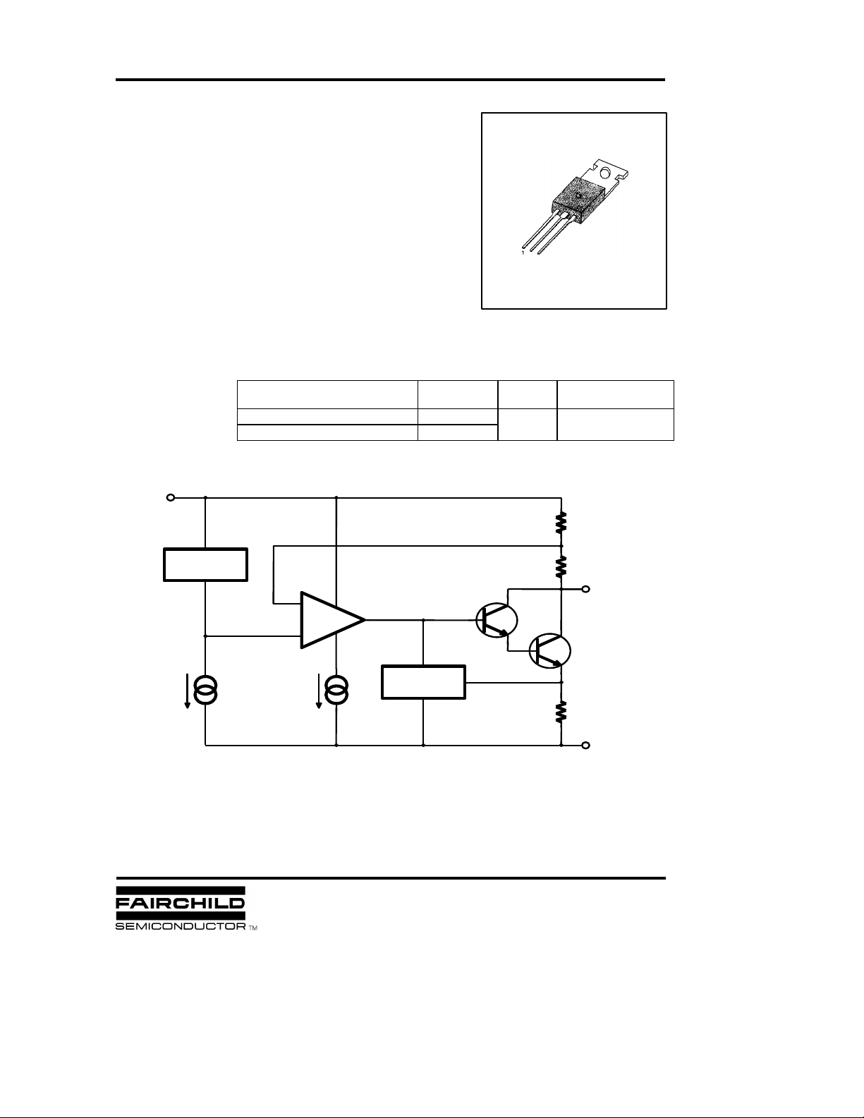
MC79XX (LM79XX) (KA79XX/A) FIXED VOLTAGE REGULATOR (NEGATIVE)
VOLTAGE
REFERENCE
+
-
PROTECTION
CIRCUITRY
R1
R2
GND
I1
I2
Out
In
Q1
Q2
ORDERING INFORMATION
BLOCK DIAGRAM
3-TERMINAL 1A NEGATIVE VOLTAGE REGULATORS
The MC79XX series of three-terminal negative regulators are available in
TO-220 package and with several fixed output voltages, making them useful
in a wide range of applications. Each type employs internal current limiting,
thermal shut-down and safe area protection, making it essentially indestructible.
TO-220
FEATURES
• Output Current in Excess of 1A
• Output Voltages of -5, -6, -8, -12, -15, -18, -24V
• Internal Thermal Overload Protection
• Short Circuit Protection
• Output Transistor Safe-Area Compensation
1: GND 2: Input 3: Output
Device Output Voltage
MC79XXCT (LM79XXCT) (KA79XX)
KA79XXA
Tolerance
± 4%
± 2%
Package Operating Temperature
TO-220
0 ~+125°C
Rsc
1999 Fairchild Semiconductor Corporation
Rev. C
Page 2

MC79XX (LM79XX) (KA79XX/A) FIXED VOLTAGE REGULATOR (NEGATIVE)
Load Regulation
∆
∆
mV
∆
ABSOLUTE MAXIMUM RATINGS (T
=+25°C, unless otherwise specified)
A
Characteristic Symbol Value Unit
Input Voltage V
Thermal Resistance Junction-Cases
Junction-Air
Operating Temperature Range T
Storage Temperature Range T
I
R
θJC
R
θJA
OPR
STG
0 ~ +125
- 65 ~ +150
LM7905 ELECTRICAL CHARACTERISTICS
(V
= 10V, lO = 500mA, 0°C ≤TJ ≤ +125°C, CI =2.2µF, CO =1µF, unless otherwise specified.)
I
Characteristic Symbol Test Conditions Min Typ Max Unit
TJ =+25°C
Output Voltage V
Line Regulation
Quiescent Current I
Quiescent Current Change
Temperature Coefficient of V
D
∆VO/∆T
Output Noise Voltage V
Ripple Rejection RR
Dropout Voltage V
Short Circuit Current I
Peak Current I
* Load and line regulation are specified at constant junction temperature. Changes in V
taken into account separately. Pulse testing with low duty is used.
IO = 5mA to 1A, PO 15W
O
VI = -7 to -20V
VI = -7 to -20V
IO=1A
VI = -8 to -12V
IO=1A
V
O
TJ =25°C
VI = -7.5 to -25V
VI= -8 to -12V
IO=1A
IO = 5mA to 1.5A
TJ =+25°C
V
O
IO = 250 to 750mA
TJ =+25°C
Q
IO = 5mA to 1A 0.05 0.5
I
Q
VI = -8 to -25V 0.1 0.8
IO = 5mA - 0.4
f = 10Hz to 100KHz
N
TA =+25°C
f = 120Hz, IO = -35V
∆VI = 10V
TJ=+25°C
D
IO = 1A
TJ =+25°C, VI = -35V
SC
TJ =+25°C
PK
-35 V
5
65
°C / W
°C /W
- 4.8 - 5.0 - 5.2
- 4.75 -5.0 - 5.25
5 50
2 25
7 50
7 50
10 100
3 50
3 6 mA
40
54 60 dB
2 V
300 mA
2.2 A
due to heating effects must be
O
°C
°C
V
mV
mA
mV/°C
µV
Page 3

MC79XX (LM79XX) (KA79XX/A) FIXED VOLTAGE REGULATOR (NEGATIVE)
∆
∆
∆
LM7906 ELECTRICAL CHARACTERISTICS
(V
= 11V, lO = 500mA, 0°C ≤TJ≤ +125°C, CI =2.2µF, CO = 1µF, unless otherwise specified.)
I
Characteristic Symbol Test Conditions Min Typ Max Unit
TJ = +25°C
Output Voltage V
IO = 5mA to 1A, PO 15W
O
VI = - 9 to - 21V
Line Regulation
TJ = 25°C
V
O
VI = - 8 to - 25V 10 120
VI= - 9 to -12V 5 60
TJ =+ 25°C
Load Regulation mV
V
O
IO = 5mA to 1.5A
TJ =+ 25°C
IO = 250 to 750mA
Quiescent Current I
Quiescent Current Change
Temperature Coefficient of V
D
∆VO/∆T
Output Noise Voltage V
Ripple Rejection RR
Dropout Voltage V
Short Circuit Current I
Peak Current I
* Load and line regulation are specified at constant junction temperature. Changes in V
taken into account separately. Pulse testing with low duty is used.
TJ =+ 25°C
Q
IO = 5mA to 1A 0.5
I
Q mA
VI = -9 to -25V 1.3
IO = 5mA -0.5
f = 10Hz to 100KHz
N
TA =+ 25°C
f = 120Hz
∆VI = 10V
TJ=+ 25°C
D
IO = 1A
TJ= +25°C, VI = -35V
SC
TJ= +25°C
PK
- 5.75 - 6 - 6.25
- 5.7 - 6 - 6.3
10 120
3 60
3 6 mA
130
54 60 dB
2 V
300 mA
2.2 A
due to heating effects must be
O
V
mV
mV/°C
µV
Page 4

MC79XX (LM79XX) (KA79XX/A) FIXED VOLTAGE REGULATOR (NEGATIVE)
∆
∆
∆
LM7908 ELECTRICAL CHARACTERISTICS
(V
= 14V, lO = 500mA, 0°C ≤TJ ≤ +125°C, CI =2.2µF, CO = 1µF, unless otherwise specified.)
I
Characteristic Symbol Test Conditions Min Typ Max Unit
TJ =+ 25°C
Output Voltage V
IO = 5mA to 1A, PO 15W
O
VI = -1.5 to -23V
Line Regulation
V
TJ = 25°C
O
VI = -10.5 to -25V 10 100
VI= -11 to -17V 5 80
TJ =+ 25°C
IO = 5mA to 1.5A
Load Regulation
V
O
TJ =+ 25°C
IO = 250 to 750mA
Quiescent Current I
Quiescent Current Change
Temperature Coefficient of V
∆VO/∆T
D
Output Noise Voltage V
Ripple Rejection RR
Dropout Voltage V
Short Circuit Current I
Peak Current I
* Load and line regulation are specified at constant junction temperature. Changes in V
into account separately. Pulse testing with low duty is used.
TJ =+ 25°C
Q
IO = 5mA to 1A 0.05 0.5
I
Q
VI = -11.5 to -25V 0.1 1
IO = 5mA -0.6
f = 10Hz to 100KHz
N
TA =+ 25°C
f = 120Hz
∆VI = 10V
TJ=+ 25°C
D
IO = 1A
TJ=+ 25°C, VI = -35V
SC
TJ=+ 25°C
PK
- 7.7 - 8 - 8.3
- 7.6 - 8 - 8.4
12 160
4 80
3 6 mA
mV/°C
175
54 60 dB
2 V
300 mA
2.2 A
due to heating effects must be taken
O
V
mV
mV
mA
µV
Page 5

MC79XX (LM79XX) (KA79XX/A) FIXED VOLTAGE REGULATOR (NEGATIVE)
∆
∆
Quiescent Current Change
∆
mA
LM7909 ELECTRICAL CHARACTERISTICS
(V
= 14V, lO = 500mA, 0°C ≤TJ ≤+ 125°C, CI =2.2µF, CO = 1µF, unless otherwise specified)
I
Characteristic Symbol Test Conditions Min Typ Max Unit
TJ =+ 25°C
Output Voltage V
IO = 5mA to 1A, PO 15W
O
VI = -1.5 to -23V
Line Regulation
V
TJ = 25°C
O
VI = -10.5 to -25V 10 180
VI= -11 to -17V 5 90
TJ =+ 25°C
IO = 5mA to 1.5A
Load Regulation
V
O
TJ =+ 25°C
IO = 250 to 750mA
Quiescent Current I
Temperature Coefficient of V
∆VO/∆T
D
Output Noise Voltage V
Ripple Rejection RR
Dropout Voltage V
Short Circuit Current I
Peak Current I
* Load and line regulation are specified at constant junction temperature. Changes in V
into account separately. Pulse testing with low duty is used.
TJ =+ 25°C
Q
IO = 5mA to 1A 0.05 0.5
I
Q
VI = -11.5 to -25V 0.1 1
IO = 5mA -0.6
f = 10Hz to 100KHz
N
TA =+ 25°C
f = 120Hz
∆VI = 10V
TJ=+ 25°C
D
IO = 1A
TJ= +25°C, VI = -35V
SC
TJ =+25°C
PK
- 8.7 - 9.0 - 9.3
- 8.6 - 9.0 - 9.4
12 180
4 90
3 6 mA
mV/°C
175
54 60 dB
2 V
300 mA
2.2 A
due to heating effects must be taken
O
V
mV
mV
µV
Page 6
MC79XX (LM79XX) (KA79XX/A) FIXED VOLTAGE REGULATOR (NEGATIVE)
∆
∆
∆
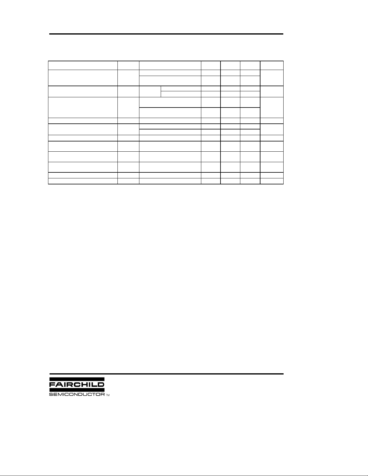
LM7912 ELECTRICAL CHARACTERISTICS
(VI= 18V, lO =500mA, 0°C ≤TJ≤ +125°C, CI =2.2µF, CO = 1µF, unless otherwise specified.)
Characteristic Symbol Test Conditions Min Typ Max Unit
TJ = +25°C
Output Voltage V
Line Regulation
IO = 5mA to 1A, PO 15W
O
VI = -15.5 to -27V
V
TJ = 25°C
O
VI = -14.5 to -30V 12 240
VI= -16 to -22V 6 120
TJ =+ 25°C
IO = 5mA to 1.5A
Load Regulation
V
O
TJ =+ 25°C
IO = 250 to 750mA
Quiescent Current I
Quiescent Current Change
Temperature Coefficient of V
∆VO/∆T
D
Output Noise Voltage V
Ripple Rejection RR
Dropout Voltage V
Short Circuit Current I
Peak Current I
* Load and line regulation are specified at constant junction temperature. Changes in V
into account separately. Pulse testing with low duty is used.
TJ =+ 25°C
Q
IO = 5mA to 1A 0.05 0.5
I
Q
VI = -15 to -30V
IO = 5mA
f = 10Hz to 100KHz
N
TA =+ 25°C
f = 120Hz
∆VI = 10V
TJ= +25°C
D
IO = 1A
TJ=+ 25°C, VI = -35V
SC
TJ=+ 25°C
PK
-11.5 -12 -12.5
-11.4 -12 -12.6
12 240
4 120
3 6 mA
0.1 1
-0.8
200
54 60 dB
2 V
300 mA
2.2 A
due to heating effects must be taken
O
V
mV
mV
mA
mV/°C
µV
Page 7
MC79XX (LM79XX) (KA79XX/A) FIXED VOLTAGE REGULATOR (NEGATIVE)
∆
∆
∆
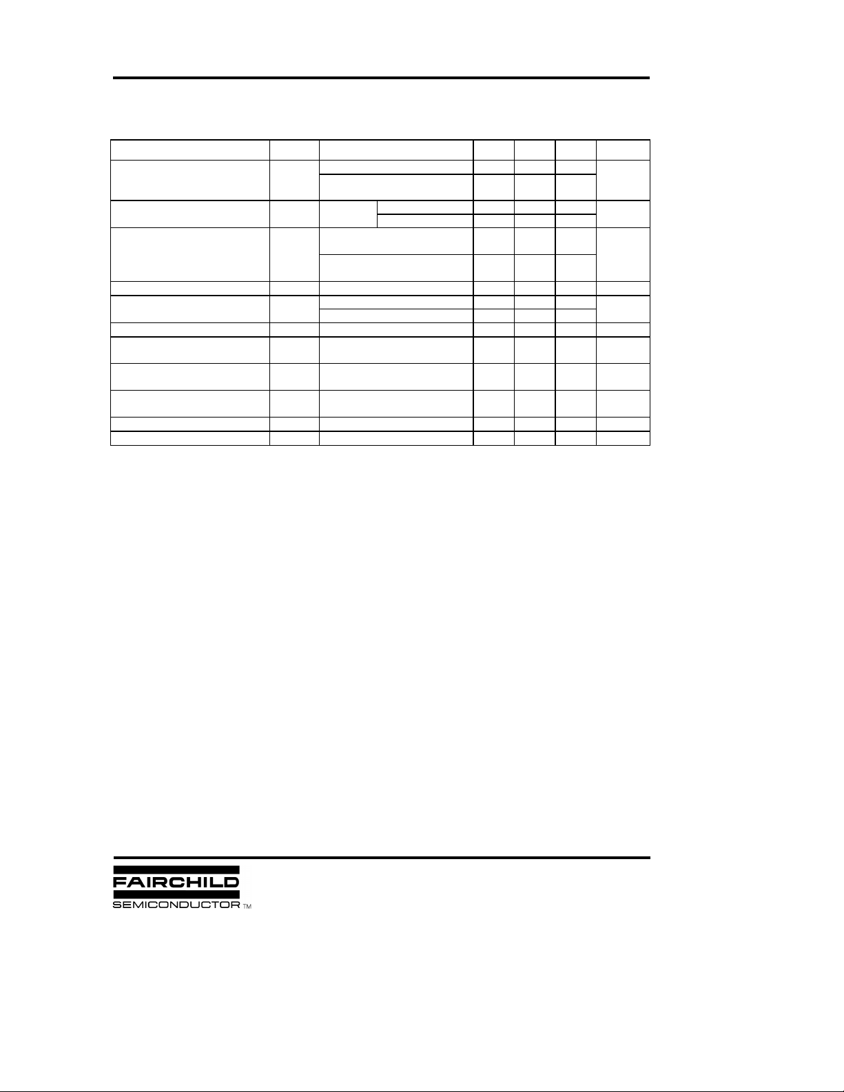
LM7915 ELECTRICAL CHARACTERISTICS
(V
= 23V, IO = 500mA, 0°C ≤TJ +125°C, CI =2.2µF, CO = 1µF, unless otherwise specified.)
I
Characteristic Symbol Test Conditions Min Typ Max Unit
TJ =+ 25°C
Output Voltage V
IO = 5mA to 1A, PO 15W
O
VI = -18 to -30V
Line Regulation
V
O
TJ = 25°C
VI = -17.5 to -30V 12 300
VI= -20 to -26V 6 150
TJ =+ 25°C
Load Regulation
IO = 5mA to 1.5A
V
O
TJ =+ 25°C
IO = 250 to 750mA
Quiescent Current I
Quiescent Current Change
Temperature Coefficient of V
∆VO/∆T
D
Output Noise Voltage V
Ripple Rejection RR
Dropout Voltage V
Short Circuit Current I
Peak Current I
TJ =+ 25°C
Q
IO = 5mA to 1A 0.05 0.5
I
Q
VI = -18.5 to -30V 0.1 1
IO = 5mA -0.9
f = 10Hz to 100Khz
N
TA =+ 25°C
f = 120Hz
∆VI = 10V
TJ=+25°C
D
IO = 1A
TJ=+ 25°C, VI = -35V
SC
TJ=+ 25°C
PK
* Load and line regulation are specified at constant junction temperature. Changes in V
into account separately. Pulse testing with low duty is used.
-14.4 -15 -15.6
-14.25 -15 -15.75
12 300
4 150
3 6 mA
mV/°C
250
54 60 dB
2 V
300 mA
2.2 A
due to heating effects must be taken
O
V
mV
mV
mA
µV
Page 8
MC79XX (LM79XX) (KA79XX/A) FIXED VOLTAGE REGULATOR (NEGATIVE)
∆
∆
∆
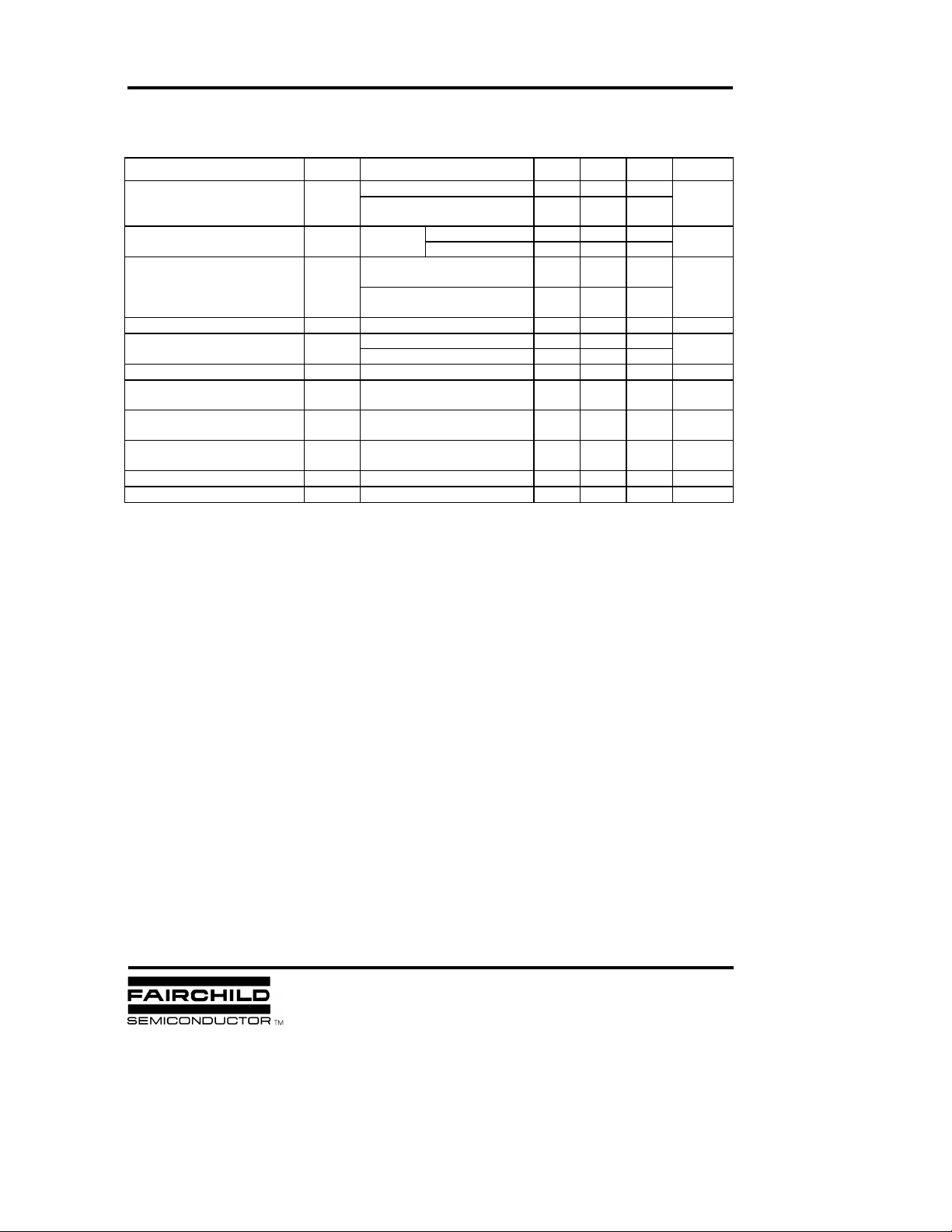
LM7918 ELECTRICAL CHARACTERISTICS
(V
= 27V, lO = 500mA, 0°C ≤TJ ≤+125°C, CI =2.2µF, CO = 1µF, unless otherwise specified.)
I
Characteristic Symbol Test Conditions Min Typ Max Unit
TJ =+ 25°C
Output Voltage V
IO = 5mA to 1A, PO 15W
O
VI = -22.5 to -33V
Line Regulation
V
O
TJ = 25°C
VI= -21 to -33V 15 360
VI= -24 to -30V 8 180
TJ =+ 25°C
IO = 5mA to 1.5A
Load Regulation
V
O
TJ =+ 25°C
IO = 250 to 750mA
Quiescent Current I
Quiescent Current Change
Temperature Coefficient of V
∆VO/∆T
D
Output Noise Voltage V
Ripple Rejection RR
Dropout Voltage V
Short Circuit Current I
Peak Current I
TJ =+ 25°C
Q
IO = 5mA to 1A 0.5
I
Q
VI = -22 to -33V 1
IO = 5mA -1
f = 10Hz to 100KHz
N
TA =+ 25°C
f = 120Hz
∆VI = 10V
TJ=+ 25°C
D
IO = 1A
TJ=+ 25°C, VI = -35V
SC
TJ=+ 25°C
PK
* Load and line regulation are specified at constant junction temperature. Changes in V
into account separately. Pulse testing with low duty is used.
-17.3 -18 -18.7
-17.1 -18 -18.9
mV
15 360
mV
5 180
3 6 mA
mA
mV/°C
300
µV
54 60 dB
2 V
300 mA
2.2 A
due to heating effects must be taken
O
V
Page 9
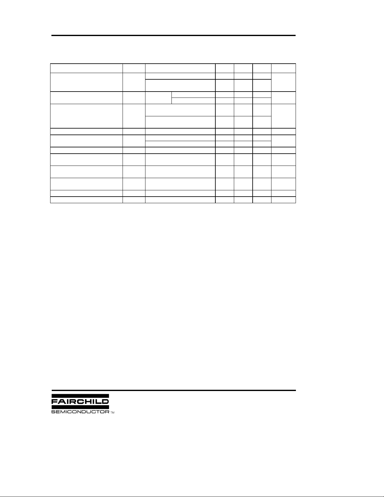
MC79XX (LM79XX) (KA79XX/A) FIXED VOLTAGE REGULATOR (NEGATIVE)
∆
∆
∆
LM7924 ELECTRICAL CHARACTERISTICS
(V
= 33V, lO = 500mA, 0°C ≤TJ ≤+125°C, CI =2.2µF, CO = 1µF, unless otherwise specified.)
I
Characteristic Symbol Test Conditions Min Typ Max Unit
Output Voltage V
IO = 5mA to 1A, PO ≤15W
O
VI = -27 to -38V
TJ =+25°C
Line Regulation
V
O
TJ = 25°C
VI = - 27 to - 38V 15 480
VI= - 30 to - 36V 8 180
TJ = +25°C
Load Regulation
IO = 5mA to 1.5A
V
O
TJ =+ 25°C
IO = 250 to 750mA
Quiescent Current I
Quiescent Current Change
Temperature Coefficient of V
∆VO/∆T
D
Output Noise Voltage V
Ripple Rejection RR
Dropout Voltage V
Short Circuit Current I
Peak Current I
TJ =+ 25°C
Q
IO = 5mA to 1A 0.5
I
Q
VI = -27 to -38V 1
IO = 5mA -1
f = 10Hz to 100KHz
N
TA =+ 25°C
f = 120Hz
∆VI = 10V
TJ= +25°C
D
IO = 1A
TJ=+ 25°C, VI = -35V
SC
TJ=+25°C
PK
* Load and line regulation are specified at constant junction temperature. Changes in V
into account separately. Pulse testing with low duty is used.
- 23 - 24 - 25
- 22.8 - 24 - 25.2
15 480
5 240
3 6 mA
mV/°C
400
54 60 dB
2 V
300 mA
2.2 A
due to heating effects must be taken
O
V
mV
mV
mA
µV
Page 10
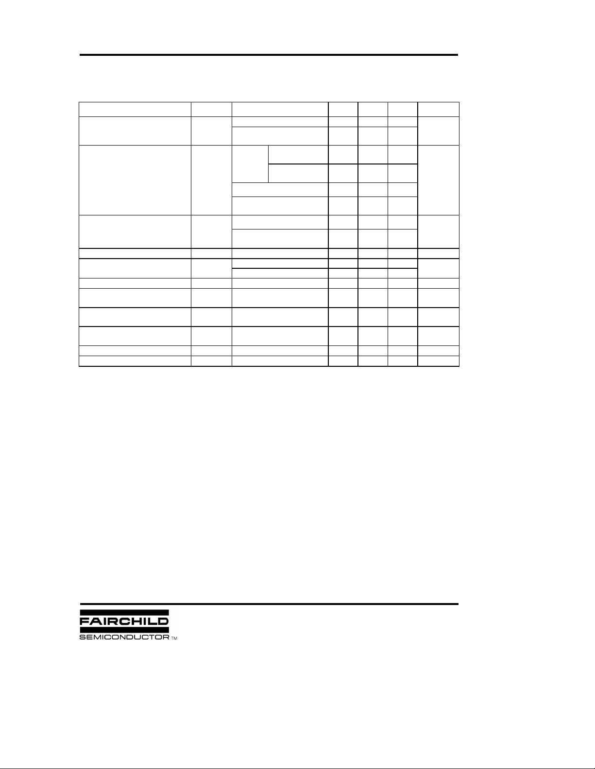
MC79XX (LM79XX) (KA79XX/A) FIXED VOLTAGE REGULATOR (NEGATIVE)
∆
∆
∆
LM7905A ELECTRICAL CHARACTERISTICS
(V
= 10V, lO = 500mA, 0°C ≤TJ ≤ +125°C, CI =2.2µF, CO =1µF, unless otherwise specified.)
I
Characteristic Symbol Test Conditions Min Typ Max Unit
TJ =+ 25°C
Output Voltage V
IO = 5mA to 1A, PO 15W
O
VI = -7 to -20V
VI = -7 to -20V
IO=1A
VI = -8 to -12V
IO=1A
Line Regulation
V
O
TJ =+25°C
VI = -7.5 to -25V
VI= -8 to -12V
IO=1A
IO = 5mA to 1.5A
Load Regulation
Quiescent Current I
Quiescent Current Change
Temperature Coefficient of V
D
∆VO/∆T
Output Noise Voltage V
Ripple Rejection RR
Dropout Voltage V
Short Circuit Current I
Peak Current I
TJ =+ 25°C
V
O
IO = 250 to 750mA
TJ = +25°C
Q
IO = 5mA to 1A 0.05 0.5
I
Q
VI = -8 to -25V 0.1 0.8
IO = 5mA - 0.4
f = 10Hz to 100KHz
N
TA =+ 25°C
f = 120Hz, IO = -35V
∆VI = 10V
TJ=+ 25°C
D
IO = 1A
TJ =+ 25°C, VI = -35V
SC
TJ =+ 25°C
PK
* Load and line regulation are specified at constant junction temperature. Changes in V
taken into account separately. Pulse testing with low duty is used.
- 4.9 - 5.0 - 5.1
- 4.8 -5.0 - 5.2
5 50
2 25
7 50
7 50
10 100
3 50
3 6 mA
mV/°C
40
54 60 dB
2 V
300 mA
2.2 A
due to heating effects must be
O
V
mV
mV
mA
µV
Page 11
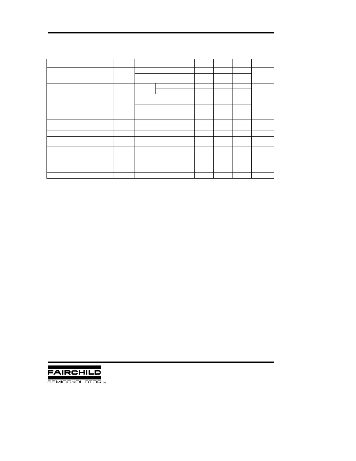
MC79XX (LM79XX) (KA79XX/A) FIXED VOLTAGE REGULATOR (NEGATIVE)
∆
∆
∆
LM7912A ELECTRICAL CHARACTERISTICS
(VI= 18V, lO =500mA, 0°C ≤TJ≤ +125°C, CI =2.2µF, CO = 1µF, unless otherwise specified.)
Characteristic Symbol Test Conditions Min Typ Max Unit
TJ =+ 25°C
Output Voltage V
Line Regulation
IO = 5mA to 1A, PO 15W
O
VI = -15.5 to -27V
V
TJ =+25°C
O
VI = -14.5 to -30V 12 240
VI= -16 to -22V 6 120
TJ = +25°C
IO = 5mA to 1.5A
Load Regulation
V
O
TJ =+ 25°C
IO = 250 to 750mA
Quiescent Current I
Quiescent Current Change
Temperature Coefficient of V
∆VO/∆T
D
Output Noise Voltage V
Ripple Rejection RR
Dropout Voltage V
Short Circuit Current I
Peak Current I
* Load and line regulation are specified at constant junction temperature. Changes in V
into account separately. Pulse testing with low duty is used.
TJ =+ 25°C
Q
IO = 5mA to 1A 0.05 0.5
I
Q
VI = -15 to -30V
IO = 5mA
f = 10Hz to 100Khz
N
TA =+ 25°C
f = 120Hz
∆VI = 10V
TJ=+ 25°C
D
IO = 1A
TJ=+ 25°C, VI = -35V
SC
TJ=+ 25°C
PK
-11.75 -12 -12.25
-11.5 -12 -12.5
12 240
4 120
3 6 mA
0.1 1
-0.8
200
54 60 dB
2 V
300 mA
2.2 A
due to heating effects must be taken
O
V
mV
mV
mA
mV/°C
µV
Page 12
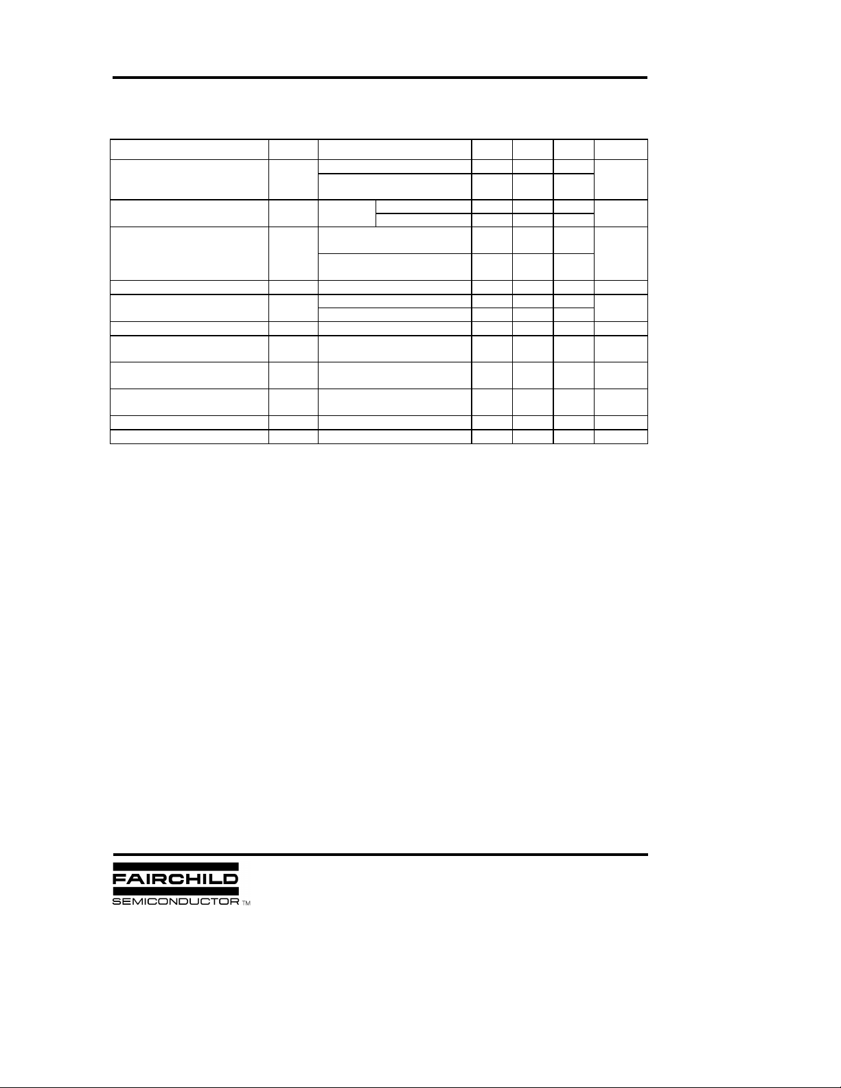
MC79XX (LM79XX) (KA79XX/A) FIXED VOLTAGE REGULATOR (NEGATIVE)
∆
∆
∆
LM7915A ELECTRICAL CHARACTERISTICS
(V
= 23V, lO = 500mA, 0°C ≤TJ≤ +125°C, CI =2.2µF, CO = 1µF, unless otherwise specified.)
I
Characteristic Symbol Test Conditions Min Typ Max Unit
TJ = +25°C
Output Voltage V
IO = 5mA to 1A, PO 15W
O
VI = -18 to -30V
Line Regulation
V
O
TJ =+25°C
VI = -17.5 to -30V 12 300
VI= -20 to -26V 6 150
TJ =+ 25°C
Load Regulation
IO = 5mA to 1.5A
V
O
TJ =+ 25°C
IO = 250 to 750mA
Quiescent Current I
Quiescent Current Change
Temperature Coefficient of V
∆VO/∆T
D
Output Noise Voltage V
Ripple Rejection RR
Dropout Voltage V
Short Circuit Current I
Peak Current I
TJ =+ 25°C
Q
IO = 5mA to 1A 0.05 0.5
I
Q
VI = -18.5 to -30V 0.1 1
IO = 5mA -0.9
f = 10Hz to 100KHz
N
TA =+25°C
f = 120Hz
∆VI = 10V
TJ= +25°C
D
IO = 1A
TJ=+ 25°C, VI = -35V
SC
TJ=+ 25°C
PK
* Load and line regulation are specified at constant junction temperature. Changes in V
into account separately. Pulse testing with low duty is used.
-14.7 -15 -15.3
-14.4 -15 -15.6
mV
12 300
mV
4 150
3 6 mA
mA
mV/°C
250
µV
54 60 dB
2 V
300 mA
2.2 A
due to heating effects must be taken
O
V
Page 13
MC79XX (LM79XX) (KA79XX/A) FIXED VOLTAGE REGULATOR (NEGATIVE)
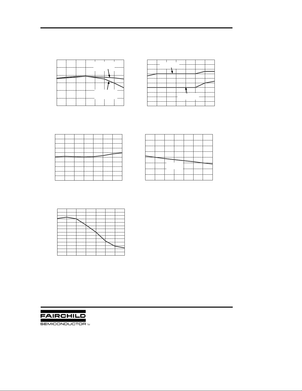
Quiescent Current [mA]
Dropout Voltage [V]
TYPICAL PERFORMANCE CHARACTERISTICS
Fig.1 Output Voltage Fig. 2 Load Regulation
5.1
5.05
5
4.95
4.9
Output Voltage [-V]
4.85
4.8
-40 -25 0 25 50 75 100 125
Vin=10V
Io=40mA
Vin=25V
Io=100mA
TA, Ambient Temperature [oC]
Fig.3 Quiescent Current Fig. 4 Dropout Voltage
5
4.5
4
3.5
3
2.5
2
1.5
1
0.5
0
-40 -25 0 25 50 75 100 125
TA, Ambient Temperature [oC] TA, Ambient Temperature [oC]
15
13
11
9
7
5
3
1
-1
Load Regulation [mV]
-3
-5
-40 -25 0 25 50 75 100 125
Io=1.5A
Io=0.75A
TA, Ambient Temperature [oC]
4
3.5
3
2.5
2
1.5
1
0.5
0
-40 -25 0 25 50 75 100 125
Io=1A
Fig.5 Short Circuit Current
0.6
0.55
0.5
0.45
0.4
0.35
0.3
0.25
0.2
0.15
0.1
0.05
0
Short Circuit Current [A]
-0.05
-0.1
-40 -25 0 25 50 75 100 125
TA, Ambient Temperature [oC]
Page 14
MC79XX (LM79XX) (KA79XX/A) FIXED VOLTAGE REGULATOR (NEGATIVE)
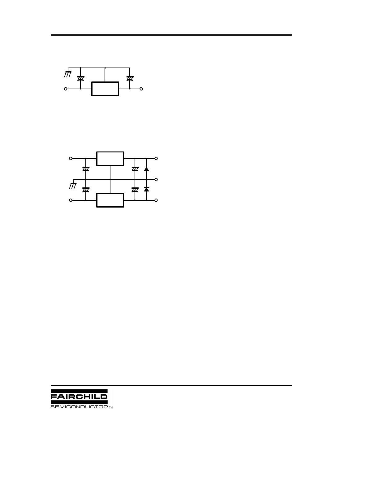
Notes:
TYPICAL APPLICATIONS
Fig. 6 Negative Fixed output regulator
(1) To specify an output voltage, substitute voltage value
2.2µµF
+ +
CI
- VI
2
1
KA79XX
1µµF
C
O
3
Fig. 7 Split power supply (±±12V/1A)
- V
O
for “XX “
(2) Required for stability. For value given, capacitor
must be solid tantalum. If aluminum electronics are
used, at least ten times value shown should be
selected. C
appreciable
distance from power supply filter.
(3) To improve transient response. If large capacitors
are used, a high current diode from input to output
(1N400l or similar) should be introduced to protect
the device from momentary input short circuit.
is required if regulator is located an
I
1
+ 15V
- 15V
KA7812
+
0.33µµF
2.2µµF
+ +
2
2
1
KA7912
*: Against potential latch-up problems.
3
1µµF
1µµF
3
1N4001
*
1N4001
*
+12V
GND
-12V
+
Page 15
TRADEMARKS
TRADEMARKS
The following are registered and unregistered trademarks Fairchild Semiconductor owns or is authorized to use and is not
The following are registered and unregistered trademarks Fairchild Semiconductor owns or is authorized to use and is not
intended to be an exhaustive list of all such trademarks.
intended to be an exhaustive list of all such trademarks.
TinyLogic™
ISOPLANAR™
ACEx™
ACEx™
CoolFET™
CoolFET™
CROSSVOLT™
CROSSVOLT™
2
2
E
E
CMOS™
CMOS™
FACT™
FACT™
FACT Quiet Series™
FACT Quiet Series™
®
®
FAST
FAST
FASTr™
FASTr™
GTO™
GTO™
HiSeC™
HiSeC™
DISCLAIMER
DISCLAIMER
FAIRCHILD SEMICONDUCTOR RESERVES THE RIGHT TO MAKE CHANGES WITHOUT FURTHER
FAIRCHILD SEMICONDUCTOR RESERVES THE RIGHT TO MAKE CHANGES WITHOUT FURTHER
NOTICE TO ANY PRODUCTS HEREIN TO IMPROVE RELIABILITY, FUNCTION OR DESIGN. FAIRCHILD
NOTICE TO ANY PRODUCTS HEREIN TO IMPROVE RELIABILITY, FUNCTION OR DESIGN. FAIRCHILD
DOES NOT ASSUME ANY LIABILITY ARISING OUT OF THE APPLICATION OR USE OF ANY PRODUCT
DOES NOT ASSUME ANY LIABILITY ARISING OUT OF THE APPLICATION OR USE OF ANY PRODUCT
OR CIRCUIT DESCRIBED HEREIN; NEITHER DOES IT CONVEY ANY LICENSE UNDER ITS PATENT
OR CIRCUIT DESCRIBED HEREIN; NEITHER DOES IT CONVEY ANY LICENSE UNDER ITS PATENT
RIGHTS, NOR THE RIGHTS OF OTHERS.
RIGHTS, NOR THE RIGHTS OF OTHERS.
LIFE SUPPORT POLICY
LIFE SUPPORT POLICY
FAIRCHILD’S PRODUCTS ARE NOT AUTHORIZED FOR USE AS CRITICAL COMPONENTS IN LIFE SUPPORT DEVICES
FAIRCHILD’S PRODUCTS ARE NOT AUTHORIZED FOR USE AS CRITICAL COMPONENTS IN LIFE SUPPORT DEVICES
OR SYSTEMS WITHOUT THE EXPRESS WRITTEN APPROVAL OF FAIRCHILD SEMICONDUCTOR CORPORATION.
OR SYSTEMS WITHOUT THE EXPRESS WRITTEN APPROVAL OF FAIRCHILD SEMICONDUCTOR CORPORATION.
As used herein:
As used herein:
1. Life support devices or systems are devices or
1. Life support devices or systems are devices or
systems which, (a) are intended for surgical implant into
systems which, (a) are intended for surgical implant into
the body, or (b) support or sustain li fe, or (c) whose
the body, or (b) support or sustain li fe, or (c) whose
failure to perform when properly used i n accordance
failure to perform when properly used i n accordance
with instructions for use provided in the labeling, can be
with instructions for use provided in the labeling, can be
reasonably expected to result in significant injury to the
reasonably expected to result in significant injury to the
user.
user.
ISOPLANAR™
MICROWIRE™
MICROWIRE™
POP™
POP™
PowerTrench
PowerTrench
QFET™
QFET™
QS™
QS™
Quiet Series™
Quiet Series™
SuperSOT™-3
SuperSOT™-3
SuperSOT™-6
SuperSOT™-6
SuperSOT™-8
SuperSOT™-8
®
2. A critical component is any component of a life
2. A critical component is any component of a life
support device or system w hose fai lure to perform can
support device or system w hose fai lure to perform can
be reasonably expected to cause the fai lure of the l ife
be reasonably expected to cause the fai lure of the l ife
support device or system, or to affect its safety or
support device or system, or to affect its safety or
effectiveness.
effectiveness.
TinyLogic™
UHC™
UHC™
VCX™
VCX™
PRODUCT STATUS DEFINITIONS
PRODUCT STATUS DEFINITIONS
Definition of Terms
Definition of Terms
Datasheet Identification Product Status Definition
Datasheet Identification Product Status Definition
Advance Information Formative or
Advance Information Formative or
Preliminary First Production This datasheet contains preliminary data, and
Preliminary First Production This datasheet contains preliminary data, and
No Identification Needed Full Production This datasheet contains final specifications. Fairchild
No Identification Needed Full Production This datasheet contains final specifications. Fairchild
Obsolete Not In Production This datasheet contains specifications on a product that has
Obsolete Not In Production This datasheet contains specifications on a product that has
In Design
In Design
This datasheet contains the design specifications for
This datasheet contains the design specifications for
product development. Specifications may change in any
product development. Specifications may change in any
manner without notice.
manner without notice.
supplementary data will be published at a later date.
supplementary data will be published at a later date.
Fairchild Semiconductor reserves the right to make
Fairchild Semiconductor reserves the right to make
changes at any time without notice in order to improve
changes at any time without notice in order to improve
design.
design.
Semiconductor reserves the right to make changes at any
Semiconductor reserves the right to make changes at any
time without notice in order to improve design.
time without notice in order to improve design.
been discontinued by Fairchild semiconductor. The
been discontinued by Fairchild semiconductor. The
datasheet is printed for reference information only.
datasheet is printed for reference information only.
 Loading...