

Page 1
©2001 Fairchild Semiconductor Corporation
www.fairchildsemi.com
Rev. 1.0.1
Features
• Output Currents up to 0.5A (output1 & 2)
• Output Current up to 1A with External Transistor
(output3)
• Fixed Precision Output 1 voltage 3.3V ± 2%
• Fixed Precision Output 2 voltage 8V ± 2% (KA7632)
• Fixed Precision Output 2 voltage 9V ± 2% (KA7633)
• Control Signal Generator for Output 3 voltage (5.1V ± 2%)
• Reset Facility for Output Voltage1
• Output 2,3 with Disable by TTL Input
• Current Limit Protection at Each Output
• Thermal Shut Down
Description
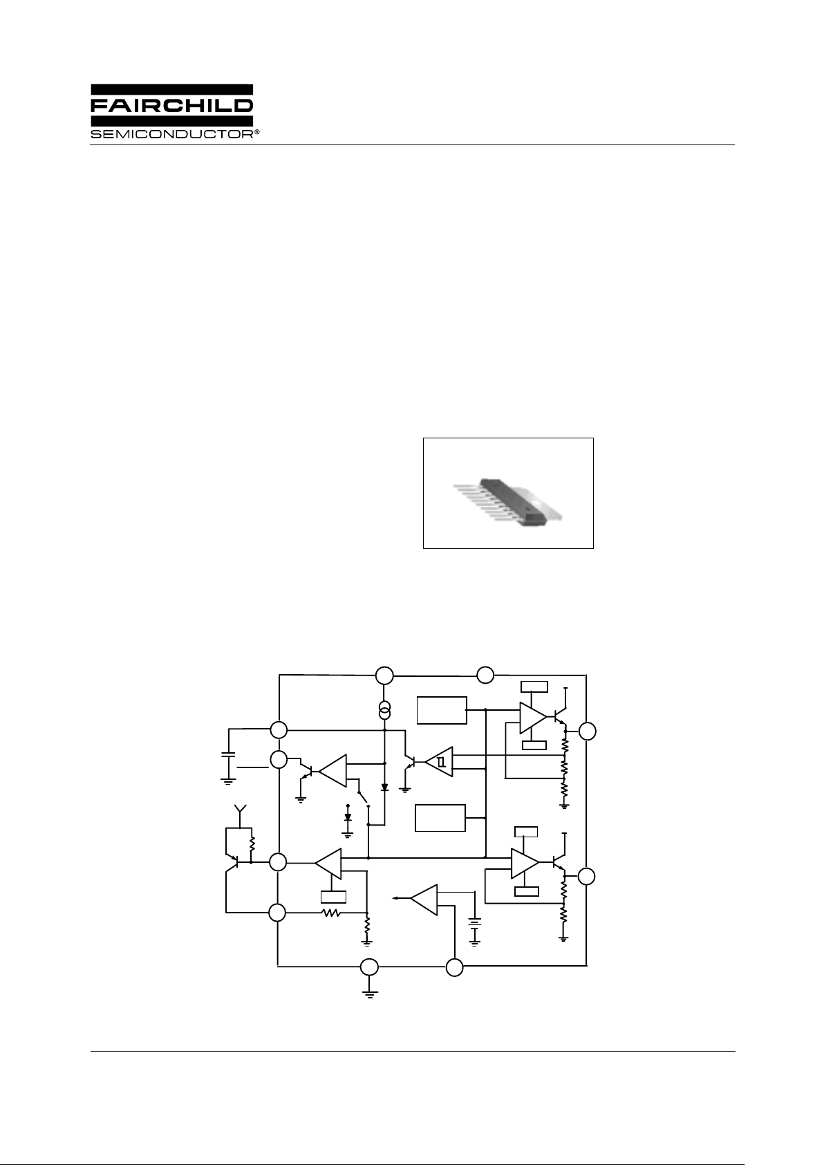
The KA7632/KA7633 is a multi-output positive voltage
regulator desi gn ed t o pr ov i de fi x e d pr e c isi on out p ut vo l ta ge s
of 3.3V, 8V (KA7632) / 9V (KA7633) at current up to 0.5A
and 5.1V at current up to 1A with external PNP transistor.
An internal reset circuit g enerates a reset pulse when the
output 1 decrease below the regulated value. Output2 & 3
can be disabled by TTL input. Protection features include
over voltage protection, short circuit protection and thermal
shutdown.
10-SIP H/S
Internal Block Diagram
Bandgap
Reference
+
-
OVP
SCP
+
-
OVP
SCP
+
-
+
-
SCP
+
-
SW
Thermal
Shut Down
Output
2,3
4
8
9
3
6
7
10
5
21
1.4V
Vsys
10uA
Vin1
Vin2
Output1
Output2
Disable
GND
Output3
Control
DEL.CAP
100nF
A614"Y"
Vin1
Vin2
+
-
RESET
10K
50mV
2.5V
Cd
KA7632/KA7633
Fixed Multi-output Regulator
Page 2
KA7632/KA7633
2
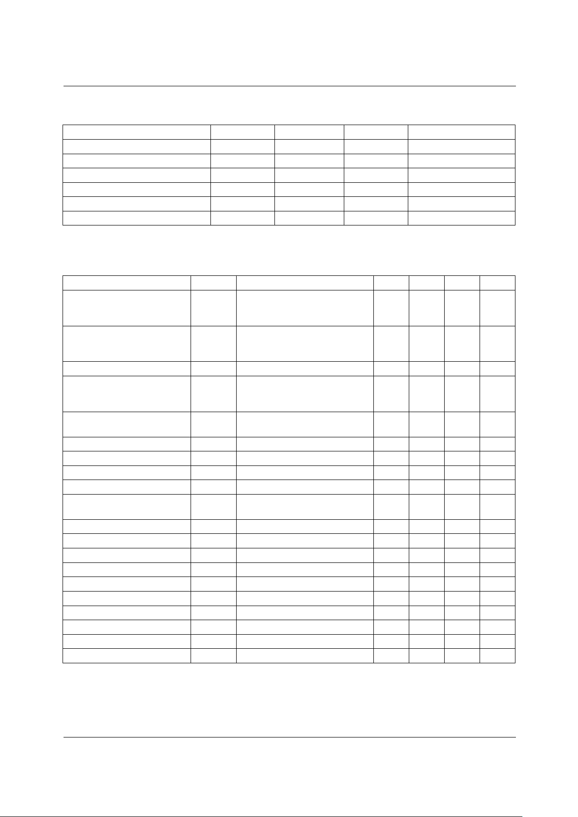
Absolute Maximum Ratings
Electrical Characteristics(KA7632)
(Refer to test circuit Vin1=6V ,Vin2=10.5V ,Tj = +25 °C, unless otherwise specified)
Notes:
1. To check the res et circuit ,the reset o utp ut is low to dischar ge th e d elay capacitor(=Cd). if it’s less than Vo 1-0.25V. And the
reset output is high when the delay capacitor voltage linearly increased by the interal current source(10µA) if it’s more than
Vo1- 0.2V. The equations of delay time is same as below. Trd = (Cd × 2.5) / 10µA
2. These parameters, although guaranteed, are not 100% tested in production.
Parameter Symbol Value Unit Remark
DC Input Voltage Vin 20 V Disable Input Voltage Vc 20 V Output Current Io 0.5 A Power Dissipation Pd 1.5 W No Heatsink
Junction Temperature Tj +150 °C-
Operating Temperature Topr 0~+125 °C-
Parameter Symbol Conditions Min. Typ. Max. Unit
Output Voltage 1 Vo1
Io1=10mA
6V<Vin1<14V
5mA<Io1<500mA
3.22
3.14
3.3
3.3
3.38
3.46
V
Output Voltage 2 Vo2
Io2=10mA
10.5V<Vin2<18V
5mA<Io2<500mA
7.84
7.7
8
8
8.16
8.3
V
Dropout Output Voltage 1,2 Vd1,2 Io1,2=500mA - - 2.5 V
Line Regulation 1,2 ∆Vo 1,2
6V <Vin1<14V
10.5V <Vin2<18V
Io1,2 = 200mA
--
40
80
mV
Load Regulation 1,2 ∆Vo 1,2
5mA < Io1< 500mA
5mA <Io2< 500mA
--
70
160
mV
Output Voltage 3 Vo3 Vsys=7V, Io3=100mA 4.97 5.1 5.23 V
Line Regulation 3 ∆Vo3 13V< Vin2 <18V, Io3 =100mA - - 50 mV
Load Regulation 3 ∆Vo3 5mA < Io3 < 1A - - 110 mV
Reset Pulse Delay Trd Cd=100nF, Note1 - 25 - ms
Saturation Voltage in Reset
Condition
VrL I6=5mA - - 0.4 V
Leakage Current at Pin 6 IrH V6=10V - - 10 µA
Output Voltage Thermal Drift STt 0 °C <Tj < +125 °C , Note 2 - 100 - ppm/°C
Short Circuit Output Current Isc1,2 Vin1=6V ,Vin2 =10.5V - - 1.6 A
Disable Voltage High VdisH Output 2 Active 2 - V
Disable Voltage Low VdisL Output 2 Disabled - - 0.8 V
Disable Bias Current Idis 0V < Vdis < 7V -100 - 2 µA
Junction Temperature for TSD Ttsd Note 2 - 145 - °C
Quiescent Current Iq Io1=10mA, Output2 Disabled - - 2 mA
Reset Threshold Voltage Vr K=Vo1 K-0.4 K-0.25 K-0.1 V
Reset Threshold Hysteresis Vrth Note 1 20 50 100 mA
Page 3
KA7632/KA7633
3
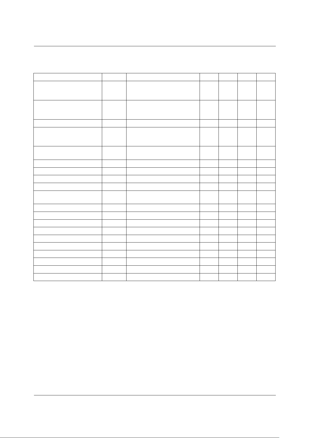
Electrical Characteristics(KA7633)
(Refer to test circuit Vin1=6V ,Vin2=11.5V ,Tj = +25 °C, unless otherwise specified)
Notes:
1. To check the res et circuit ,the reset output is low to d i sc ha rge the delay capacitor (= Cd ). if it’s less than V o1 -0.2 5V . And the
reset output is high when the delay capacitor voltage linearly increased by the interal current source(10µA) if it’s more than
Vo1- 0.2V. The equations of delay time is same as below. Trd = (Cd × 2.5) / 10µA
2. These parameters, although guaranteed, are not 100% tested in production.
Parameter Symbol Conditions Min. Typ. Max. Unit
Output Voltage 1 Vo1
Io1=10mA
6V<Vin1<14V
5mA<Io1<500mA
3.22
3.14
3.3
3.3
3.38
3.46
V
Output Voltage 2 Vo2
Io2=10mA
11.5V<Vin2<18V
5mA<Io2<500mA
8.82
8.65
9
9
9.18
9.35
V
Dropout Output Voltage 1,2 Vd1,2 Io1,2=500mA - - 2.5 V
Line Regulation 1,2 ∆Vo 1,2
6V <Vin1<14V
11.5V <Vin2<18V
Io1,2 = 200mA
--
40
80
mV
Load Regulation 1,2 ∆Vo 1,2
5mA < Io1< 500mA
5mA <Io2< 500mA
--
70
160
mV
Output Voltage 3 Vo3 Vsys=7V, Io3=100mA 4.97 5.1 5.23 V
Line Regulation 3 ∆Vo3 13V< Vin2 <18V, Io3 =100mA - - 50 mV
Load Regulation 3 ∆Vo3 5mA < Io3 < 1A - - 110 mV
Reset Pulse Delay Trd Cd=100nF, Note1 - 25 - ms
Saturation Voltage in Reset
Condition
VrL I6=5mA - - 0.4 V
Leakage Current at Pin 6 IrH V6=10V - - 10 µA
Output Voltage Thermal Drift STt 0 °C <Tj < +125 °C , Note 2 - 100 - ppm/°C
Short Circuit Output Current Isc1,2 Vin1=6V ,Vin2 =11.5V - - 1.6 A
Disable Voltage High VdisH Output 2 Active 2 - V
Disable Voltage Low VdisL Output 2 Disabled - - 0.8 V
Disable Bias Current Idis 0V < Vdis < 7V -100 - 2 µA
Junction Temperature for TSD Ttsd Note 2 - 145 - °C
Quiescent Current Iq Io1=10mA, Output2 Disabled - - 2 mA
Reset Threshold Voltage Vr K=Vo1 K-0.4 K-0.25 K-0.1 V
Reset Threshold Hysteresis Vrth Note 1 20 50 100 mA
Page 4
KA7632/KA7633
4
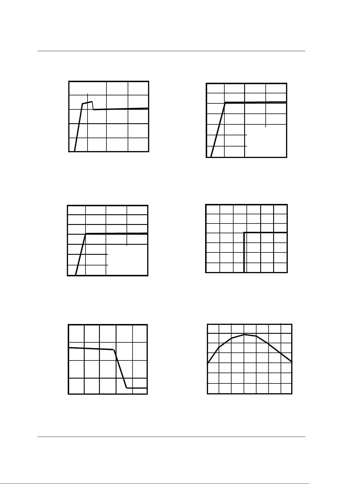
Typical Perfomance Characteristics
Figure 1. Quiescent Cu rre nt vs. Inpu t Vo lta ge
Figure 3. Output Voltage2 vs. Input Voltage
Figure 5. Disable Bias Current vs. Disable Voltage
Figure 2. Output Voltage1 vs. Input Voltage
Figure 4. Output Voltage vs. Disa ble Voltage High(Low)
Figure 6. Output Voltage1 vs. Temperature(Tj)
0155
10
2.0
1.6
1.2
0.8
0.4
0
Quiescent current Iq( mA)
Input voltage Vin (V)
20
TJ = 25oC
Io1 =10mA
Input Voltage Vi n (V)
Input voltage Vin (V)
10 15
12
10
8
6
4
2
14
0
0
Output voltage2 Vo(V)
205
TJ = 25oC
Io1 =10mA
10.5V<Vin1<18V
5mA<Io1<500mA
2
2
2
Disable Voltage(V)
40
30
20
10
0
Disable Bias Current( uA)
0 0.4 0.8 1.2 1.6 2.0
10 15
6
5
4
3
2
1
7
0
0
Output voltage1 Vo(V)
205
TJ = 25oC
Io1 =10mA
7.5V<Vin1<14V
5mA<Io1<500mA
Input Voltage Vin (V)
6
Output volt age Vo(V )
14
12
10
8
6
0
030.5
1.5
4
2
122.5
Disable Voltage ( V)
Temperature Tj(
℃
)
5.10
5.095
5.09
5.105
-25
Output voltage1 Vo(V)
75
125
02550
100
5.08
5.075
5.07
5.085
Page 5
KA7632/KA7633
5
Typical Perfomance Characteristics (continued)
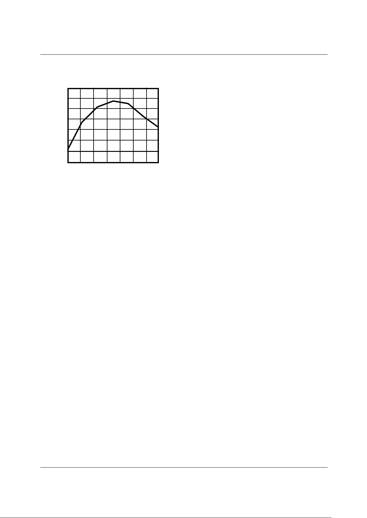
Figure 7. Output Voltage2 vs. Temperature(Tj)
Temperature Tj(℃)
8.06
8.05
8.04
8.07
-25
75
125
02550
100
8.02
8.01
8.00
8.03
150
Page 6
KA7632/KA7633
6
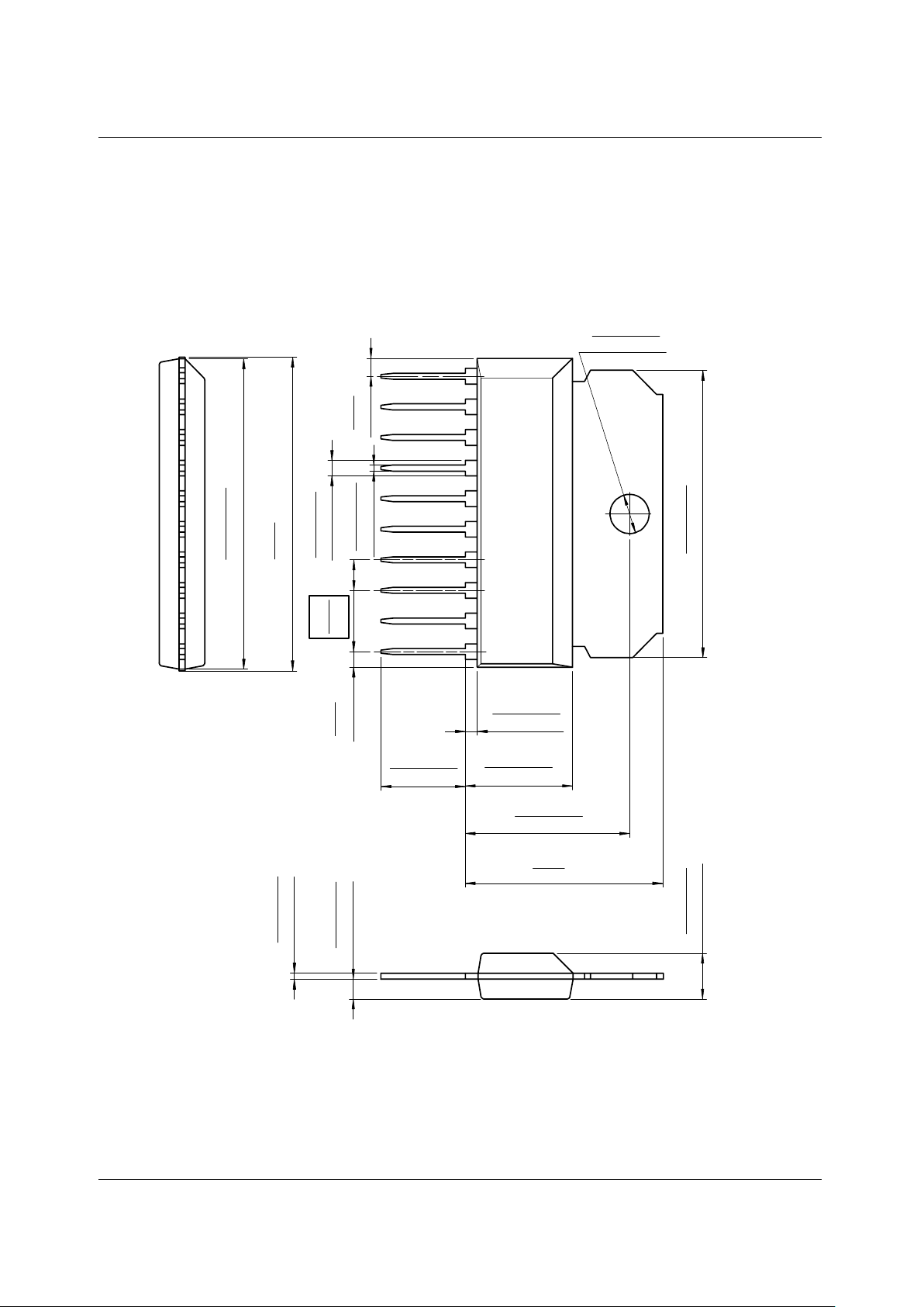
Mechanical Dimensions
Package
Dimensions in millimeters
#1
#10
25.75 ±0.10
1.013 ±0.004
26.05
1.026
MAX
1.30 ±0.10
0.051 ±0.004
0.50 ±0.10
0.020 ±0.004
1.65 ±0.10
0.065 ±0.004
3.80 ±0.20
0.150 ±0.008
0.50 ±0.10
0.020 ±0.004
23.86 ±0.20
0.939 ±0.008
1.50
0.059
()
1.30
0.051
()
2.54
0.100
7.00 ±0.30
0.276 ±0.012
8.90 ±0.20
0.350 ±0.008
1.00 ±0.20
0.039 ±0.008
3.25 ±0.20
0.128 ±0.008
13.65 ±0.30
0.537 ±0.012
16.80
0.661
MAX
10-SIP H/S
Page 7

KA7632/KA7633
7
Ordering Information
Product Number Package Operating Temperature
KA7632
10-SIP H/S 0°C to +125°C
KA7633
Page 8

KA7632/KA7633
8/1/01 0.0m 001
Stock#DSxxxxxxxx
2001 Fairchild Semiconductor Corporation
LIFE SUPPORT POL I CY
FAIRCHILD’S PRODUCTS ARE NOT AUTHORIZED FOR USE AS CRITICAL COMPONENTS IN LIFE SUPPORT DEVICES
OR SYSTEMS WITHOUT THE EXPRESS WRITTEN APPROVAL OF THE PRESIDENT OF FAIRCHILD SEMICONDUCTOR
CORPORATION. As used herein :
1. Life support devices or systems are devices or systems
which, (a) are intended for surgical implant into the body,
or (b) support or sustain life, and (c) whose failure to
perform when properly used in accordance with
instructions for use provided in the labeling, can be
reasonably expected to result in a significant injury of the
user.
2. A critical component in any component of a life support
device or sys tem whose failure to perform can be
reasonably expec ted to cause the failur e of the life support
device or system, or to affect its safety or effec tiveness.
www.fairchildsemi.com
DISCLAIMER
FAIRCHILD SEMICONDUCTOR RESERVES THE RIGHT TO MAKE CHANGES WITHOUT FURTHER NOTICE TO ANY
PRODUCTS HEREI N TO IMPROVE RELIABILITY, FUNCTION OR DES IGN. FAIRCHILD DOES NOT ASSUME ANY
LIABILITY ARISING OUT OF THE APPLICATION OR USE OF ANY PRODUCT OR CIRCUIT DESCRIBED HEREIN; NEITHER
DOES IT CONVEY ANY LICENSE UNDER ITS PATENT RIGHTS, NOR THE RI GHTS OF OTHERS.
 Loading...