

Page 1

©2000 Fairchild Semiconductor International
www.fairchildsemi.com
Rev. 5.0
Features
• Short circuit protection
• Excellent temperature stability
• Internal frequency compensation
• High Input vo ltage range
• Null of offset
Description
The KA741/KA741E series are general purpose operational
amplifiers. It is intended for a wide range of analog applications. The high gain and wide range of operating voltage
provide superior performance in intergrator, summing
amplifier, and general feedback applications.
8-DIP
8-SOP
1
1
Internal Block Diagram
KA741/KA741E
Single Operational Amplifier
Page 2

KA741/KA741E
2
Schematic Diagram
Absolute Maximum Ratings (T
A
= 25°C)
Parameter Symbol KA741 KA741E Unit
Supply Voltage V
CC
±18 ±22 V
Differential Input Voltage V
I(DIFF)
30 30 V
Input Voltage V
I
±15 ±15 V
Output Short Circuit Duration - Indefinite Indefinite
Power Dissipation P
D
500 500 mW
Operating Temperature Range T
OPR
0 ~ + 70 0 ~ + 70 °C
Storage Temperature Range T
STG
-65 ~ + 150 -65 ~ + 150 °C
Page 3

KA741/KA741E
3
Electrical Characteristics
(V
CC
= 15V, V
EE
= - 15V. TA = 25
°C, unless otherwise specified)
Parameter Symbol Conditions
KA741E KA741
Unit
Min. Typ. Max. Min. Typ. Max.
Input Offset Voltage V
IO
R
S
≤
10K
Ω
----2.06.0
mV
R
S
≤50Ω
0.8 3.0 - - -
Input Offset Voltage
Adjustment Range
V
IO(R)VCC
= ±20V
±
10---±15 - mV
Input Offset Current I
IO
-
- 3.0 30 - 20 200 nA
Input Bias Current I
BIAS
-
-3080-80500nA
Input Resistance R
I
VCC =±20V 1.0 6.0 - 0.3 2.0 - M
Ω
Input Voltage Range V
I(R)
-
±12±
13 -
±12±
13 - V
Large Signal Voltage Gain G
V
R
L
≥2KΩ
V
CC
=±20V,
V
O(P-P)
=±15V 50
----V/mV
VCC =±15V,
V
O(P-P)
=±10V
- - - 20 200 -
Output Short Circuit Current I
SC
- 10 25 35 - 25 - mA
Output Voltage Swing V
O(P-P)
VCC = ±20V R
L
≥
10K
Ω±
16-----
V
R
L
≥
10K
Ω±
15-----
V
CC
= ±15V R
L
≥
10K
Ω
---±12±14 -
R
L
≥
10K
Ω
---±10±13 -
Common Mode Rejection
Ratio
CMRR
R
S
≤
10KΩ, V
CM
= ±12V - - - 70 90 -
dB
R
S
≤50Ω
, V
CM
= ±12V 80 95 - - - -
Power Supply Rejection
Ratio
PSRR
VCC = ±15V to VCC = ±15V
R
S
≤50Ω
86 96 - - - -
dB
V
CC
= ±15V to VCC = ±15V
R
S
≤
10K
Ω
---7796-
Transient Rise Time t
R
Unity Gain
- 0.25 0.8 - 0.3 -
µ
s
Response Overshoot OS - 6.0 20 - 10 - %
Bandwidth BW
-
0.43 1.5 - - - - MHz
Slew Rate SR Unity Gain 0.3 0.7 - - 0.5 - V/µs
Supply Current I
CC
RL=
∞Ω
----1.52.8mA
Power Consumption P
C
VCC = ±20V - 80 150 - - -
mW
V
CC
= ±15V - - - - 50 85
Page 4

KA741/KA741E
4
Electrical Characteristics
( 0°C ≤T
A
≤70 °C V
CC
= ±15V, unless otherwise specified)
Parameter Symbol Conditions
KA741E KA741
Unit
Min. Typ. Max. Min. Typ. Max.
Input Offset Voltage V
IO
R
S
≤50Ω --4.0---
mV
R
S
≤10KΩ -----7.5
Input Offset Voltage Drift ∆V
IO
/∆T - -15- - - µV/
°C
Input Offset Current I
IO
- - - 70 - - 300 nA
Input Offset Current Drift ∆I
IO
/∆T - --0.5-- nA/
°C
Input Bias Current I
BIAS
- - - 0.21 - - 0.8 µA
Input Resistance R
I
V
CC
= ±20V 0.5 - - - - - MΩ
Input Voltage Range V
I(R)
- ±12 ±13 - ±12 ±13 - V
Output Voltage Swing V
O(P-P)
VCC =±20V
R
S
≥10KΩ±16 - - - - -
V
R
S
≥2KΩ±15 - - - - -
V
CC
=±15V
R
S
≥10KΩ ---±12 ±14 -
R
S
≥2KΩ ---±10 ±13 -
Output Short Circuit
Current
I
SC
- 10 - 40 10 - 40 mA
Common Mode Rejection
Ratio
CMRR
R
S
≤10KΩ, V
CM
= ±12V - - - 70 90 -
dB
R
S
≤50Ω, V
CM
= ±12V 80 95 - - - -
Power Supply Rejection
Ratio
PSRR
V
CC
= ±20V
to ±5V
R
S
≤50Ω 86 96 - - - -
dB
R
S
≤10KΩ ---7796-
Large Signal Voltage
Gain
G
V
R
S
≥2KΩ
V
CC
= ±20V,
V
O(P-P)
= ±15V
32 - - - - -
V/mV
V
CC
= ±15V,
V
O(P.P)
= ±10V
---15- -
V
CC
= ±15V,
V
O(P-P)
= ±2V
10 - - - - -
Page 5
KA741/KA741E
5
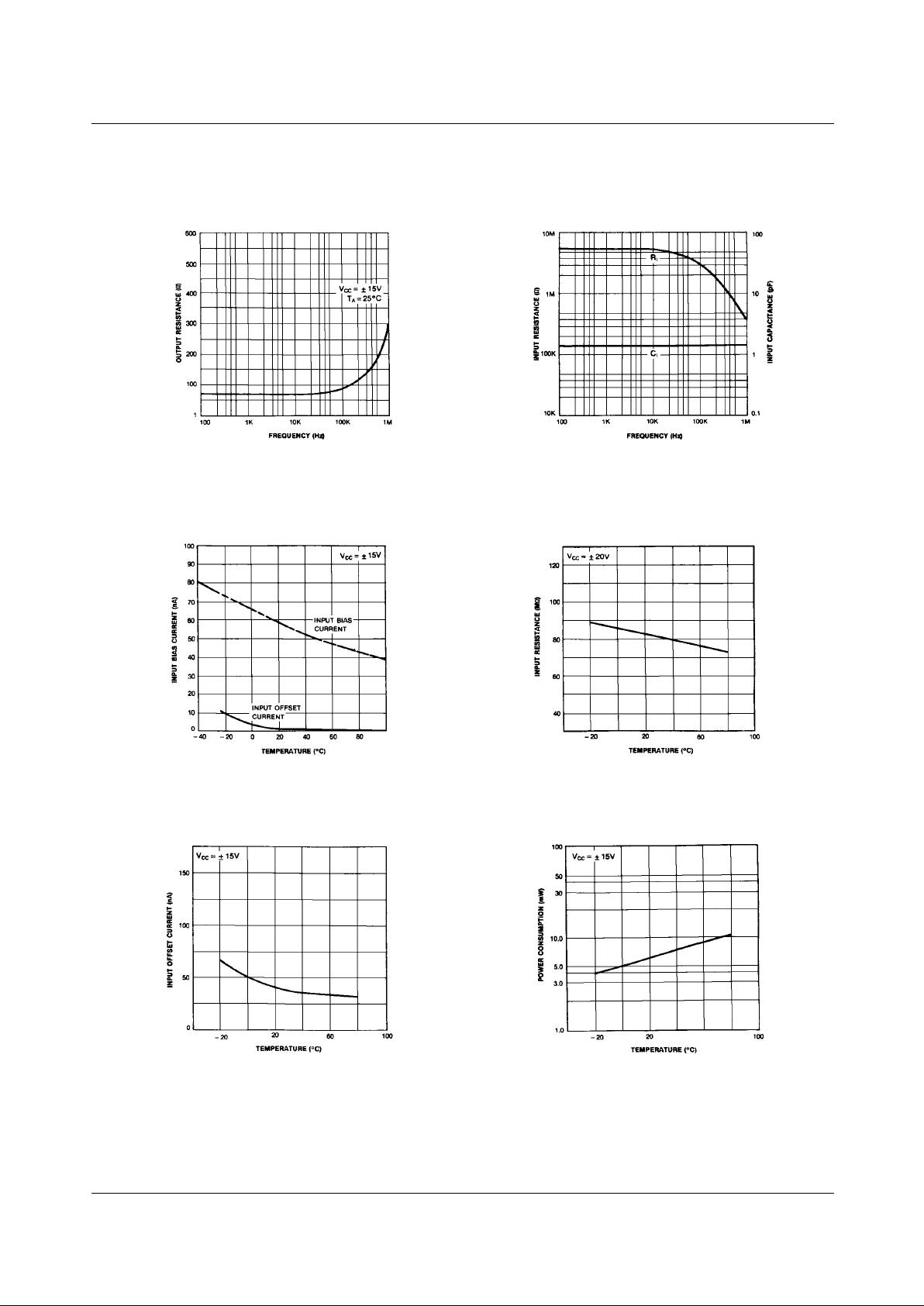
Typical Performance Characteristics
Figure 1. Output Resistance vs Frequency Figure 2. Input Resistance and Input
Capacitance vs Frequency
Figure 3. Input Bias Current vs Ambient Temperature Figure 4. Power Comsumption vs Ambient Temperature
Figure 5. Input Offset Current vs Ambient Temperature Figure 6. Input Resistance vs Ambient Temperature
Page 6
KA741/KA741E
6
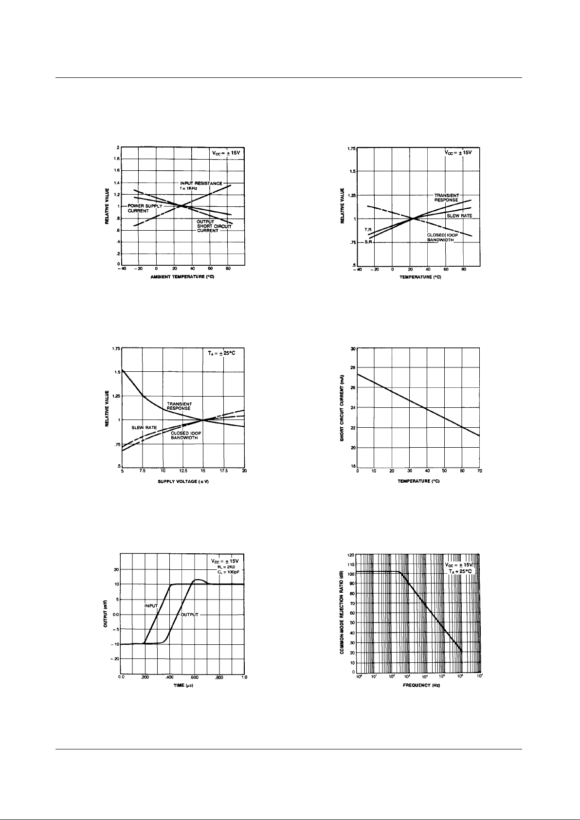
Typical Performance Characteristics (continued)
Figure 7. Normalized DC Parameters vs
Ambient Temper atu r e
Figure 8. Frequency Ch aracteristics vs
Ambient Temperature
Figure 9. Frequency Characteristics vs Supply Voltage Figure 10. Output Short Circuit Current vs
Ambient Temperature
Figure 11. Transient Response Figure 12. Common-Mode Rejection Ratio
vs Frequency
Page 7
KA741/KA741E
7
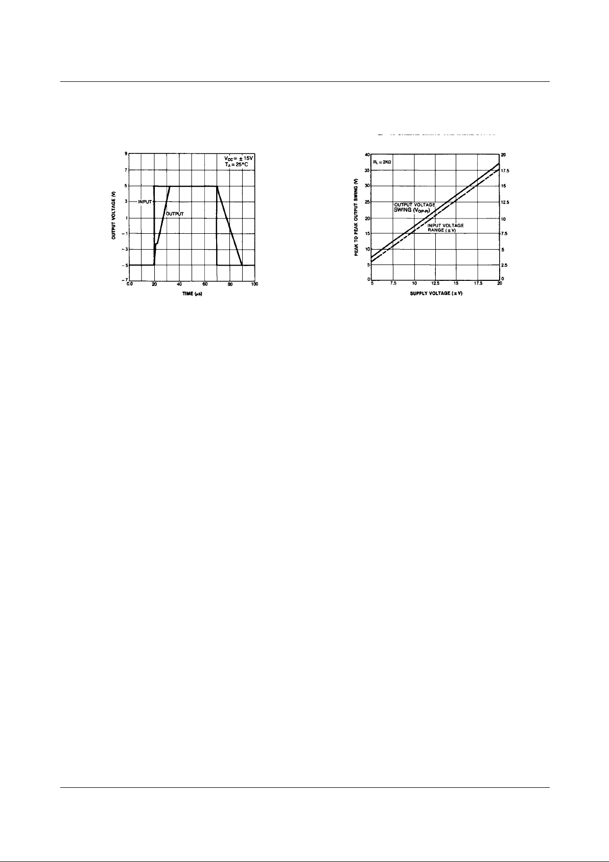
Typical Performance Characteristics (continued)
Figure 13. Voltage Follower Large Si gnal Pulse Response Figure 14. Output Swing and Input Range
vs Supply Voltage
Page 8
KA741/KA741E
8
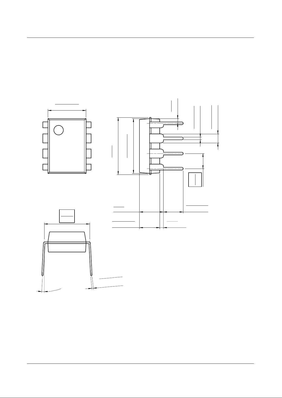
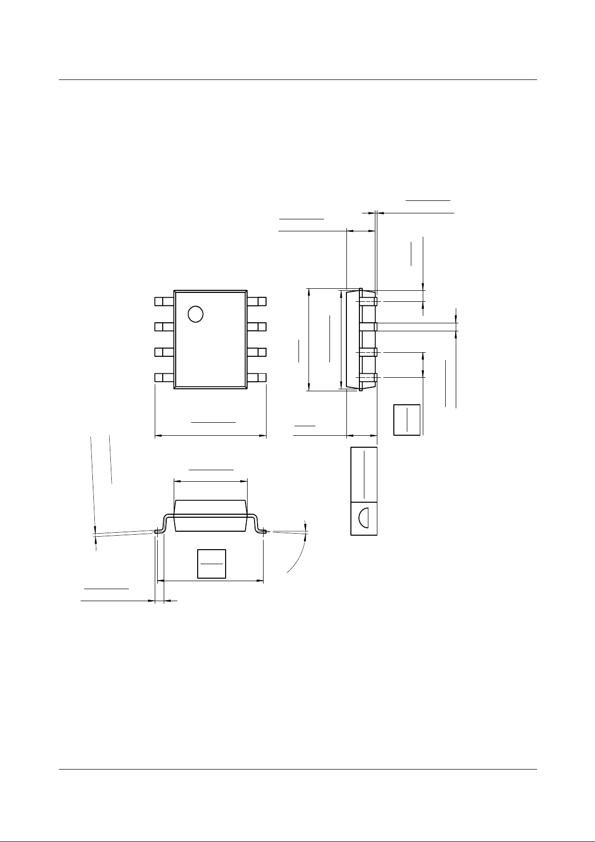
Mechanical Dimensions
Package
6.40
±0.20
3.30
±0.30
0.130
±0.012
3.40
±0.20
0.134
±0.008
#1
#4 #5
#8
0.252
±0.008
9.20
±0.20
0.79
2.54
0.100
0.031
()
0.46
±0.10
0.018
±0.004
0.060
±0.004
1.524
±0.10
0.362
±0.008
9.60
0.378
MAX
5.08
0.200
0.33
0.013
7.62
0~15°
0.300
MAX
MIN
0.25
+0.10
–0.05
0.010
+0.004
–0.002
8-DIP
Page 9
KA741/KA741E
9
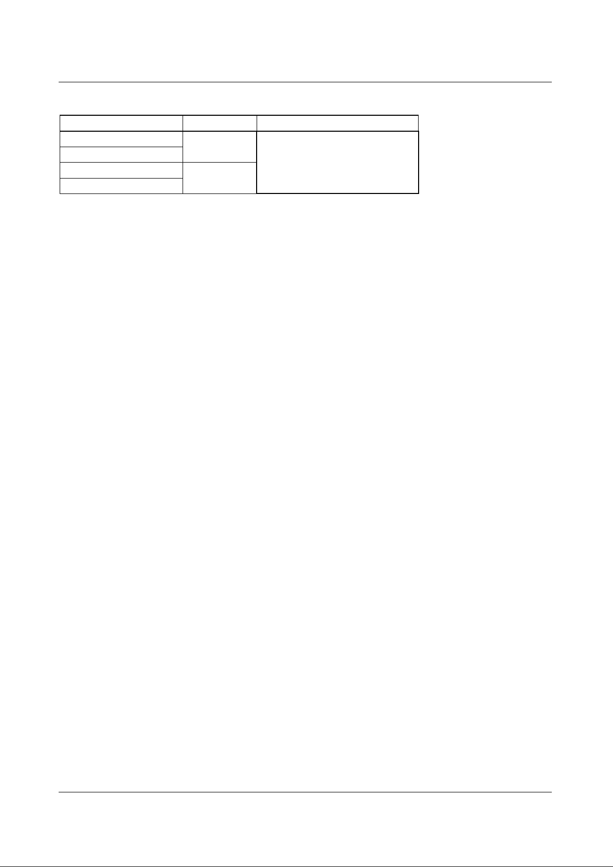
Mechanical Dimensions
(Continued)
Package
4.92
±0.20
0.194
±0.008
0.41
±0.10
0.016
±0.004
1.27
0.050
5.72
0.225
1.55
±0.20
0.061
±0.008
0.1~0.25
0.004~0.001
6.00
±0.30
0.236
±0.012
3.95
±0.20
0.156
±0.008
0.50
±0.20
0.020
±0.008
5.13
0.202
MAX
#1
#4
#5
0~8°
#8
0.56
0.022
()
1.80
0.071
MAX0.10
MAX0.004
MAX
MIN
+
0.10
-0.05
0.15
+
0.004
-0.002
0.006
8-SOP
Page 10
KA741/KA741E
10
Ordering Information
Product Number Package Operating Temperature
KA741
8 DIP
0 ~ + 70°C
KA741E
KA741D
8 SOP
KA741ED
Page 11

KA741/KA741E
11
Page 12

KA741/KA741E
7/13/00 0.0m 001
Stock#DSxxxxxxxx
2000 Fairchild Semiconductor International
LIFE SUPPORT POL I CY
FAIRCHILD’S PR ODUCTS ARE NOT AUTH ORIZED FOR USE AS C RITICAL COMPONENT S IN LIFE SUPPORT DE VICES
OR SYSTEMS WITHOUT THE EXPRESS WRITTEN APPROVAL OF THE PRESIDENT OF FAIRCHILD SEMICONDUCTOR
INTERNATIONAL. As used herein:
1. Life support devices or systems are devices or systems
which, (a) are intended for surgical implant into the body,
or (b) support or sustain life, and (c) whose failure to
perform when properly used in accordance with
instructions for use provided in the labeling, can be
reasonably expected to result in a significant injury of the
user.
2. A critical component in any component of a life support
device or sy stem whose fai lure to perform can be
reasonably expec ted to cause the failur e of the life support
device or system, or to affect its safety or effec t iv ene ss .
www.fairchildsemi.com
 Loading...