

Page 1
KA556
Dual Timer
www.fairchildsemi.com
Features
• Replaces Two KA555 Timers
• Operates in Both Astable And Monostable Modes
•High Output Current
• TTL Compatible
• Timing From Microsecond To Hours
• Adjustable Duty Cycle
• Temperature Stability Of 0.005% Per °C
Applications
• Precision Timing
• Pulse Shaping
• Pulse Width Modulation
• Frequency Division
• Traffic Light Control
• Sequential Timing
• Pulse Generator
• Time Delay Generator
• Touch Tone Encoder
• Tone Burst Generator
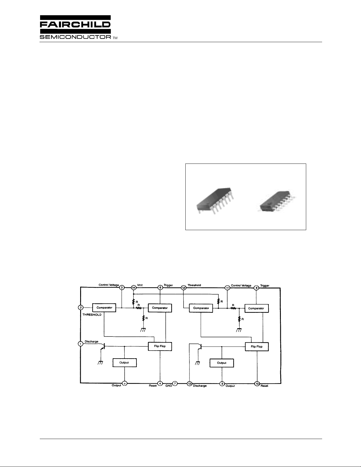
Internal Block Diagram
Description
The KA556 series dual monolithic timing circuits are a
highly stable controller capable of producing accurate time
delays or oscillation. The KA556 is a dual KA555. Timing is
provided an external resistor and capacitor for each tim ing
function. The two timers operate independently of each
other, sharing only V
triggered and reset on falling waveforms. The output
structures may sink or source 200mA.
14-DIP
1
and ground. The circuits may be
CC
14-SOP
1
©2001 Fairchild Semiconductor Corporation
Rev. 1.0.0
Page 2
KA556
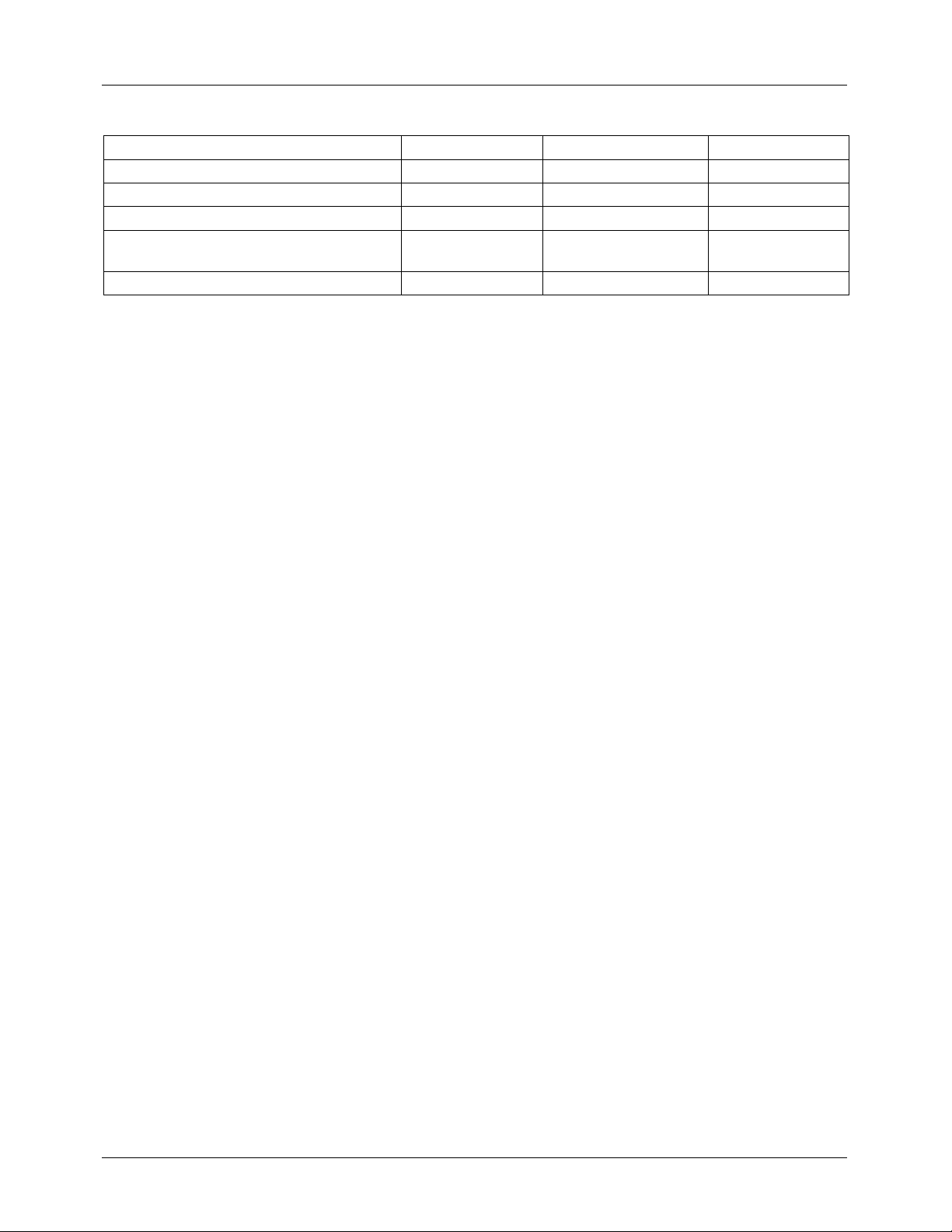
Absolute Maximum Ratings (TA = 25°°°°C)
Parameter Symbol Value Unit
Supply Voltage V
Lead Temperature (soldering 10sec) T
Power Dissipation P
Operating Temperature Range
KA556 T
Storage Temperature Range T
CC
LEAD
D
OPR
STG
16 V
300 °C
600 mW
0 ~ + 70 °C
- 65 ~ + 150 °C
2
Page 3
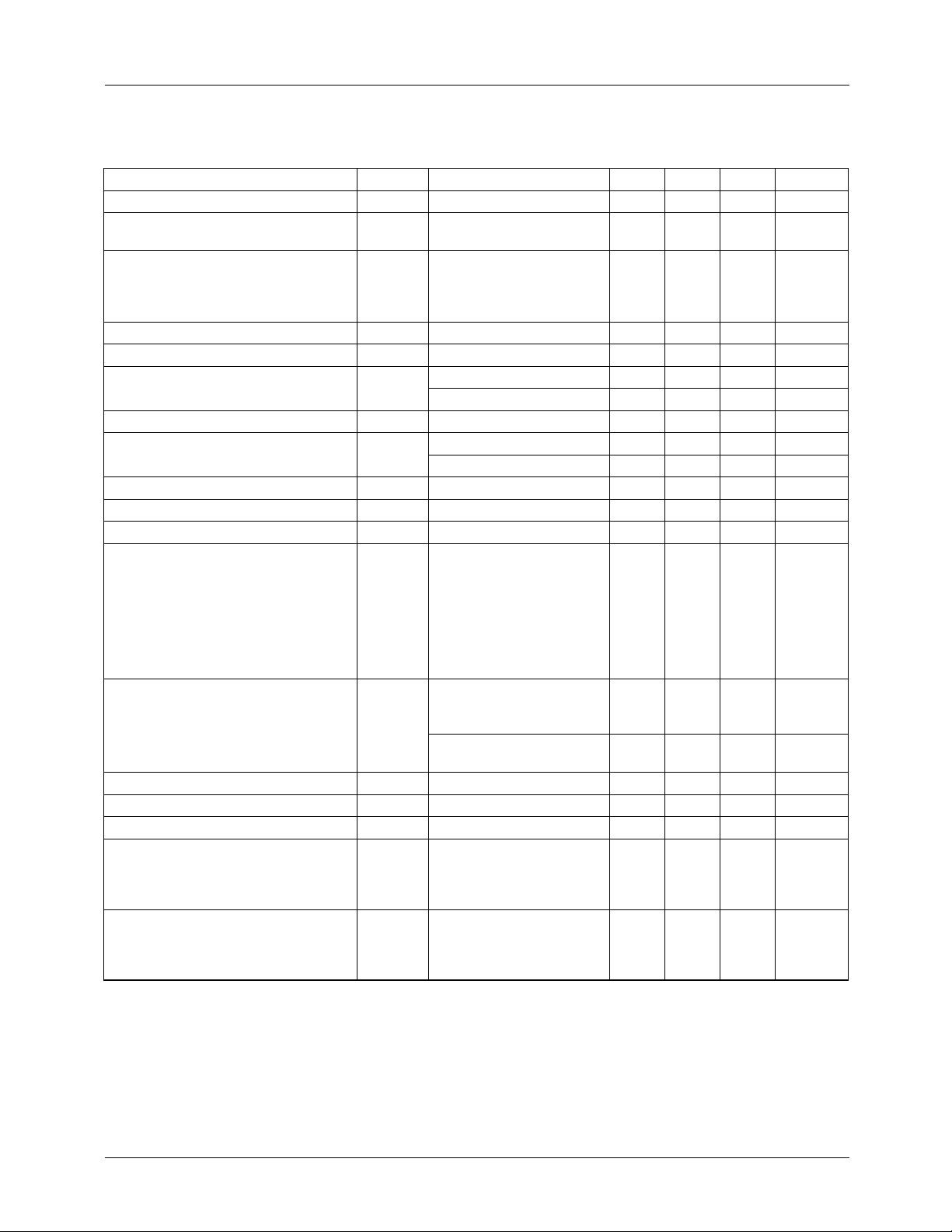
Electrical Characteristics
(TA = 25°C, VCC = 5 ~ 15V, unless otherwise specified)
Parameter Symbol Conditions Min. Typ. Max. Unit
Supply Voltage V
Supply Current *
(two timers)
1
(low state)
Timing Error *
(monostable)
2
Initial Accuracy
Drift with Temperature
Drift with Supply Voltage
Control Voltage V
Threshold Voltage V
Threshold Current*
3
Trigger Voltage V
Trigger Current I
Reset Voltage*
5
Reset Current I
Low Output Voltage V
High Output Voltage V
Rise Time of Output t
Fall Time of Output t
Discharge Leakage Current I
Matching Characteristics*
4
Initial Accuracy
Drift with Temperature
Drfit with Supply Voltage
2
Timing Error (astable)*
Initial Accuracy
Drift with Temperature
Drift with Supply Voltage
CC
I
CC
ACCUR
∆t/∆T
∆t/∆V
CC
C
TH
I
TH
TR
TR
V
RST
RST
OL
OH
R
F
LKG
ACCUR
∆t/∆T
∆t/∆V
CC
ACCUR
∆t/∆T
∆t/∆Vcc
VCC = 5V, RL = ∞
V
CC
R
A
C = 0.1µF
T = 1.1RC
VCC = 15V 9.0 10.0 11.0 V
V
CC
VCC = 15V 8.8 10.0 11.2 V
V
CC
VCC = 15V 4.5 5.0 5.6 V
V
CC
V
TR
VCC = 15V
I
SINK
I
SINK
I
SINK
I
SINK
V
CC
I
SINK
I
SINK
VCC = 15V
I
I
V
CC
I
V
CC
R
A,RB
C = 0.1µF
-4.5-16V
= 15V, RL = ∞
= 2KΩ to 100KΩ
-
-
5
16
0.75
50
12
30
-
0.1
= 5V 2.6 3.33 4.0 V
= 5V 2.4 3.33 4.2 V
- - 30 250 nA
= 5V 1.1 1.6 2.2 V
= 0V - 0.01 2.0 µA
- 0.4 0.6 1.0 V
- - 0.03 0.6 mA
= 10mA
= 50mA
= 100mA
= 200mA
-
0.1
0.4
2.0
2.5
0.25
0.75
3.2
= 5V
= 8mA
= 5mA
SOURCE
SOURCE
= 5V
SOURCE
= 200mA
= 100mA 12.75
= 100mA 2.75 3.3
0.25
0.15
12.5
13.3
0.35
0.25
-V
-
- - 100 300 ns
- - 100 300 ns
- - 10 100 nA
--
= 15V
= 1KΩ to 100KΩ
1.0
10
0.2
2.25
-
150
2.0
0.5
-
0.3
KA556
mA
mA
%
ppm/°C
%/V
V
V
V
%
ppm/°C
%/V
%
ppm/°C
%/V
Notes:
*1. Supply curr ent when output is high is typically 1.0m A less at V
*2. Tested at V
*3. This will determine the maxi mum value of R
The maximum total R = 20MΩ, and for 5V operation the maximum total R = 6.6MΩ.
*4. Matching characteristics refer to the difference between performance characteristics of each timer section in the monostable
mode.
*5. As reset voltage lowers, timing is inhibited and then the output goes low.
= 5V and VCC = 15V
CC
+ RB for 15V operation.
A
CC
= 5V
3
Page 4
KA556
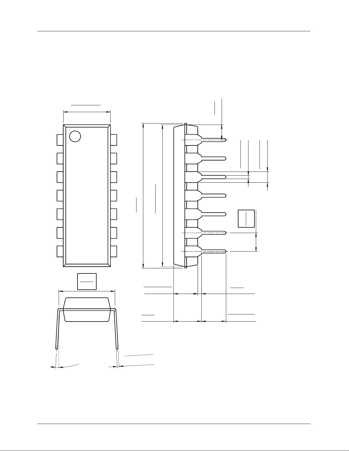
Mechanical Dimensions
Package
6.40 ±0.20
±0.008
0.252
14-DIP
2.08
0.082
()
#1
#7
7.62
0.300
#14
#8
MAX
19.80
0.780
3.25 ±0.20
0.128 ±0.008
19.40 ±0.20
0.764 ±0.008
±0.10
0.46
0.20
0.008
0.018 ±0.004
2.54
MIN
1.50 ±0.10
0.100
0.059 ±0.004
3.30 ±0.30
0.130 ±0.012
0~15°
0.25
0.010
5.08
0.200
+0.10
–0.05
+0.004
–0.002
MAX
4
Page 5
KA556
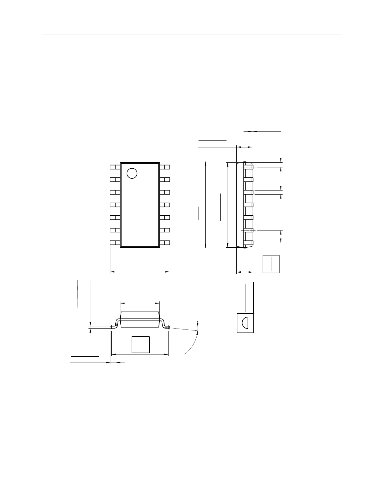
Mechanical Dimensions
Package
#1
(Continued)
14-SOP
#14
1.55 ±0.10
0.061 ±0.004
MAX
8.70
0.343
8.56 ±0.20
0.337 ±0.008
MIN
0.05
0.002
0.47
()
0.004
-0.05
+0.10
+
0.406
0.019
-0.002
0.016
0.10
0.004
+
-0.05
+
-0.002
0.20
0.008
0.60 ±0.20
0.024 ±0.008
#7
6.00 ±0.30
0.236 ±0.012
3.95 ±0.20
0.156 ±0.008
5.72
0.225
#8
0~8°
1.80
0.071
MAX
MAX0.10
MAX0.004
1.27
0.050
5
Page 6

KA556
Ordering Information
Product Number Package Operating Temperature
KA556 14-DIP
KA556D 14-SOP
KA556I 14-DIP
KA556ID 14-SOP
0 ~ + 70°C
6
Page 7

KA556
7
Page 8

KA556
DISCLAIMER
FAIRCHILD SEMICONDUCTOR RESERVES THE RIGHT TO MAKE CHANGES WITHOUT FURT HER NOTICE TO ANY
PRODUCTS HEREI N TO IMPROVE RELIABILITY, FUNCTIO N OR DESIGN. FAIRCH IL D DOES NOT ASSUME ANY
LIABILITY ARISING OUT OF THE APPLICATION OR USE OF ANY PRODUCT OR CIRCUIT DESCRIBED HEREIN; NEITHER
DOES IT CONVEY ANY LICENSE UNDER IT S PATENT RIGHTS, NOR THE RIGHTS OF OTHE RS.
LIFE SUPPORT POL I CY
FAIRCHILD’S PR ODUCTS ARE NOT AUTH ORIZED FOR USE AS C RITICAL COMPONENT S IN LIFE SUPPORT DE VICES
OR SYSTEMS WITHOUT THE EXPRESS WRITTEN APPROVAL OF THE PRESIDENT OF FAIRCHILD SEMICONDUCTOR
CORPORATION. As used herein :
1. Life support devices or systems are devices or systems
which, (a) are intended for surgical implant into the body,
or (b) support or sustain life, and (c) whose failure to
perform when properly used in accordance with
2. A critical component in any component of a life support
device or sy stem whose fai lure to perform can be
reasonably expec ted to cause the failur e of the life support
device or system, or to affect its safety or effec t iv ene ss .
instructions for use provided in the labeling, can be
reasonably expected to result in a significant injury of the
user.
www.fairchildsemi.com
5/22/01 0.0m 001
2001 Fairchild Semiconductor Corporation
Stock#DSxxxxxxxx
 Loading...