

Page 1
KA2822D
3-Phase BLDC Motor Driver
www.fairchildsemi.com
Features
• 3-phase, full-wave, linear BLDC motor driver
with 2 hall sensors
• Built-in soft switching drive circuit
• 300 or 360 RPM speed control
• Snubberless
• Built-in chip enable function
• Built-in digital speed control circuit
• Built-in current limit circuit
• Index sensorless
• Built-in TSD (Thermal shutdown)
• Low saturation voltage
• Digital input: TTL, 5V CMOS compatible
• Built-in current-mode control circuit (I
PEAK
Description
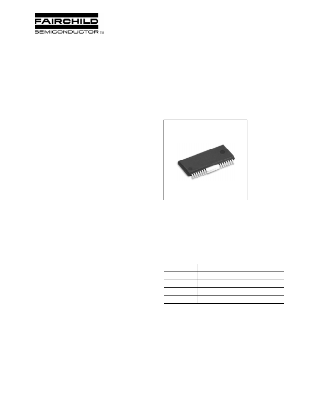
The KA2822D is a monolithic integrated circuit, and suitable for the three-phase spindle motor driver of FDD system.
28-SSOPH-375
: 1A)
Typical Application
• 3.5-inch floppy disk drive (FDD) spildle motor
• Other 3-phase BLDC motor
©2000 Fairchild Semiconductor International
Ordering Information
Device Package Operating Temp.
KA2822D 28-SSOPH-375 0 ~ 75°C
KA2822DTF 28-SSOPH-375 0 ~ 75°C
KA2822BD 28-SSOPH-375 0 ~ 75°C
KA2822BDTF 28-SSOPH-375 0 ~ 75°C
Rev. 1.0.1
May. 2000.
1
Page 2
KA2822D
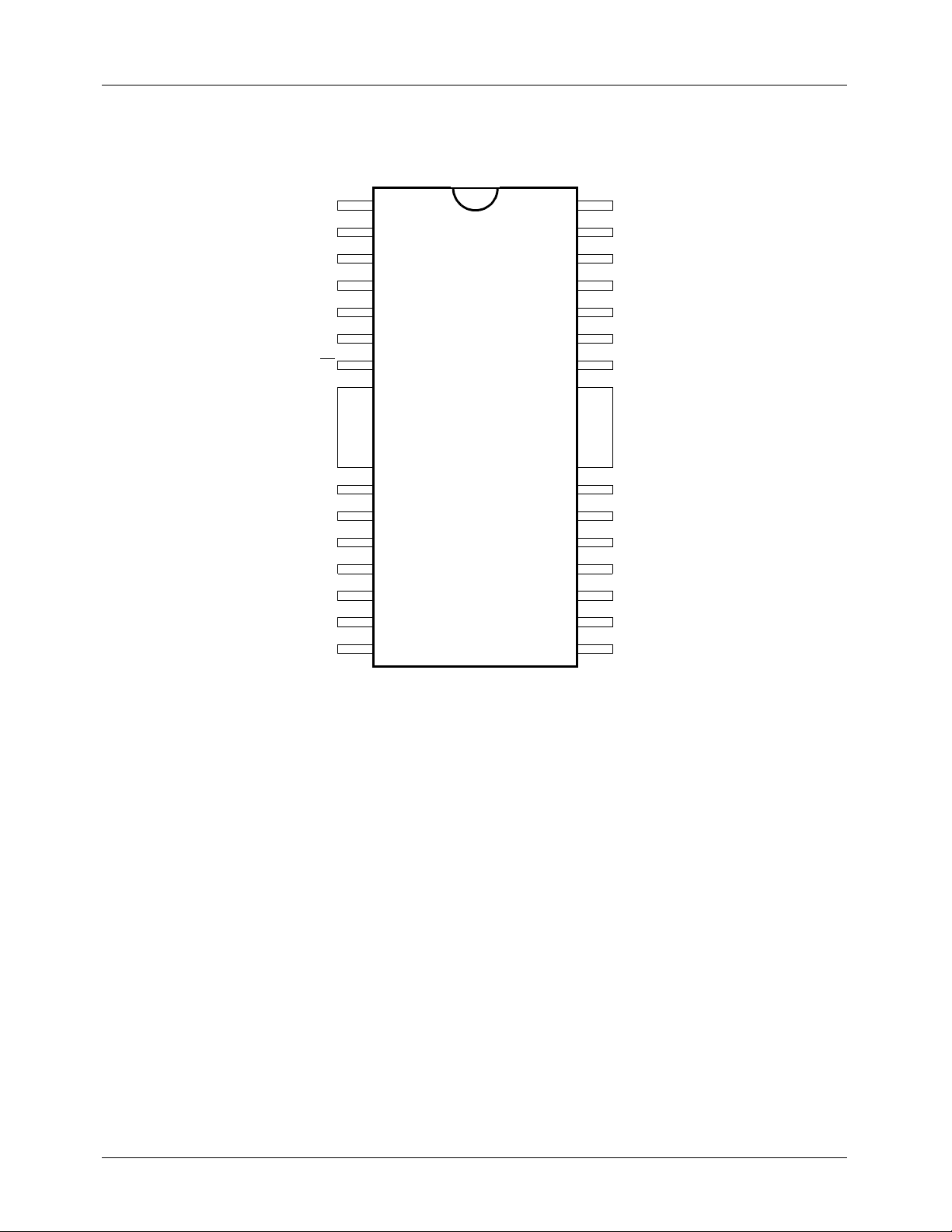
Pin Assignments
FG INPUT(−)
AGC
INDEX PULSE WIDTH
VOLTAGE REG
INDEX BURST
INDEX OUTPUT
CE
SIGNAL GROUND
FG ZERO CROSS
FG OUTPUT
RPM SELECT
CHARGE PUMP OUTPUT
OSC INPUT
NC
1
2
3
4
5
6
7
28
27
26
25
24
23
22
KA2822D
8
9
10
11
12
13
14
21
20
19
18
17
16
15
FG INPUT(+)
HALL BIAS
CURRENT DETECTION1
V INPUT(−)
V INPUT(+)
U PHASE OUTPUT
V PHASE OUTPUT
FINFIN
W PHASE OUTPUT
NC
U INPUT(+)
U INPUT(−)
CURRENT DETECTION2
V
CC
PHASE COMPENSATION
2
Page 3

Pin Definitions
Pin Number Pin Name I/O Pin Function Description
1 FG_INPUT I Negative input pin FG signal amp.
2 AGC I Automatic gain control input pin
3 INDEX PULSE WIDTH O Index pulse width detection (1.1V) pin
4 VOLTAGE REGULATOR O Voltage (2.2V) generator output pin
5 INDEX BURST O Index pulse width detection (1.4V) pin
6 INDEX OUTPUT O Index pulse output pin
7 CE I Chip enable (Active low)
8 SIGNAL GROUND - Signal ground
9 FG ZERO CROSS O FG signal zero cross detection pin
10 FG OUTPUT O FG signal output pin
11 RPM SELECT I RPM selection pin (L: 300, H: 360rpm)
12 CHARGE PUMP OUTPUT O Charge pump output pin
13 OSC INPUT I 1MHz oscillation input pin
14 NC - No connection
15 PHASE COMPENSATION I Phase compensation cap. connection pin
16 V
17 CURRENT DETECTION2 I Over current detection pin
18 U INPUT (−) I Negative input pin of U phase amp
19 U INPUT (+) I Positive input pin of U phase amp
20 NC - No connection
21 W PHASE OUTPUT O W phase output pin
22 V PHASE OUTPUT O V phase output pin
23 U PHASE OUTPUT O U phase output pin
24 U INPUT (+) I Positive input pin of V phase amp
25 V INPUT (−) I Negative input pin of V phase amp
26 CURRENT DETECTION1 I Over current detection pin
27 HALL BIAS I Hall sensor bias input pin
28 FG INPUT (+) I Positive input pin of FG signal amp
FIN POWER GROUND - Power ground
CC
- 5V power supply pin
KA2822D
3
Page 4
KA2822D
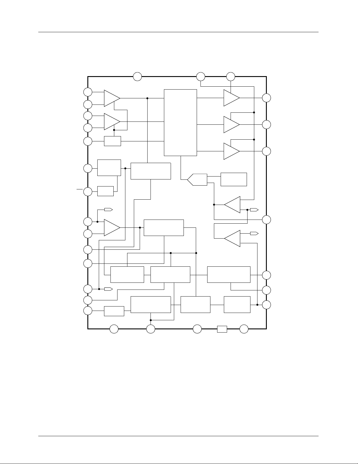
Internal Block Diagram
U INPUT (+)
U INPUT(−)
V INPUT (+)
V INPUT(−)
AGC
HALL BIAS
CE
FG INPUT(+)
FG INPUT(−)
FG OUTPUT
Output
Control
CURRENT
DETECTION2
V
CC
16 17 26
19
18
24
25
2
27
7
28
1
10
+
U_AMP
−
+
V_AMP
−
AGC
Start-up
CE
FG_AMP
+
−
1.3V
Hall
Zero-cross
FG
Zero-cross
CURRENT
DETECTION1
U_OUT
V_OUT
W_OUT
CON_AMP
BUF_AMP
TSD
23
U PHASE
OUTPUT
22
U PHASE
OUTPUT
21
W PHASE
OUTPUT
−
+
0.24V
15
PHASE
COMPENSATION
−
0.69V
+
FG ZERO
CROSS
VOLTAGE REG.
INDEX BURST
OSC INPUT
9
Timing
Detectpr
4
5
13
2.2V
Rpm_select
OSC
NC RPM SIGNAL NCFIN
11_divider
Burst_time
Circuit
Speed
Control
SELECT GROUND
Pulse_width
Adjustment
Charge
Pump
6
INDEX
OUTPUT
3
INDEX PULSE
WIDTH
12
CHARGE
PUMP
OUTPUT
2081114
4
Page 5
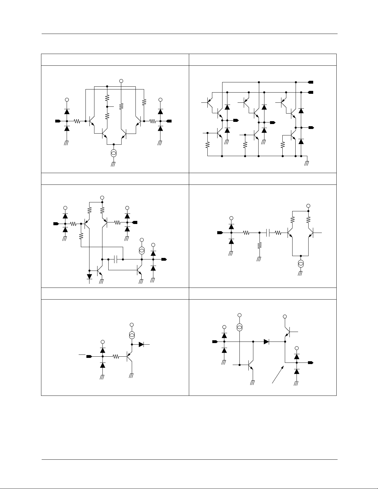
Equivalent Circuits
vcc
vcc
U_amp, V_ amp input U, V, W drive output and current detection 1, 2
vcc
5k
Ω
vcc
KA2822D
(17Pin,
26Pin)
V
CC
(16Pin)
(19Pin,
25Pin)
vcc
2.5k
Ω
2.5k
Ω
(18Pin,
U
(23Pin)
24Pin)
40k
Ω
40k
Ω
FG input and FG output OSC input
vcc
0.5k
25k
0.5k
Ω
Ω
Ω
(28Pin)
vcc
(13Pin)
vcc
(10Pin)
CE input Hall bias input and voltage regulator output
vcc
0.1k
V
40k
(22Pin)
Ω
W
(21Pin)
vcc
Ω
5k
Ω
50pF
1k
Ω
CE
vcc
vcc
vcc
(27Pin)
3k
Ω
vcc
vcc
2.9V
vcc
(4Pin)
2.2V
5
Page 6
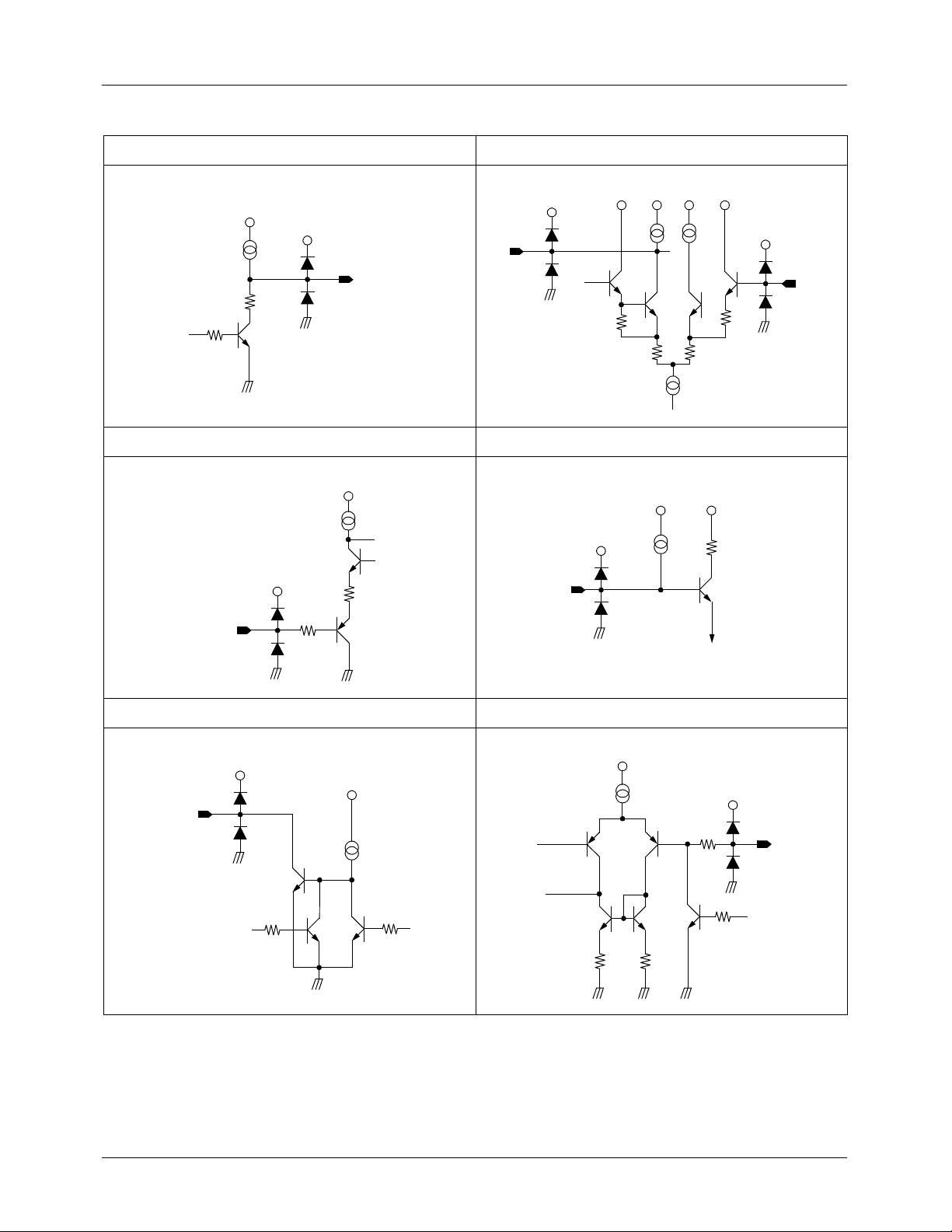
KA2822D
vcc
vcc
vcc
vcc
vcc
vcc
Equivalent Circuits (Continued)
Index pulse width detection output Phase compensation and current detection 1, 2
vcc
vcc
vcc
(15Pin)
(3Pin)
2k
Ω
2k
Ω
RPM select input AGC input
vcc
vcc
AGC
(2Pin)
(11Pin)
6k
Ω
vcc
vcc
vcc
To U amp, V amp
(Current control)
(17Pin,
26Pin)
(6Pin)
Index output Index burst output
vcc
vcc
1.4V
vcc
2k
Ω
(5Pin)
6
Page 7
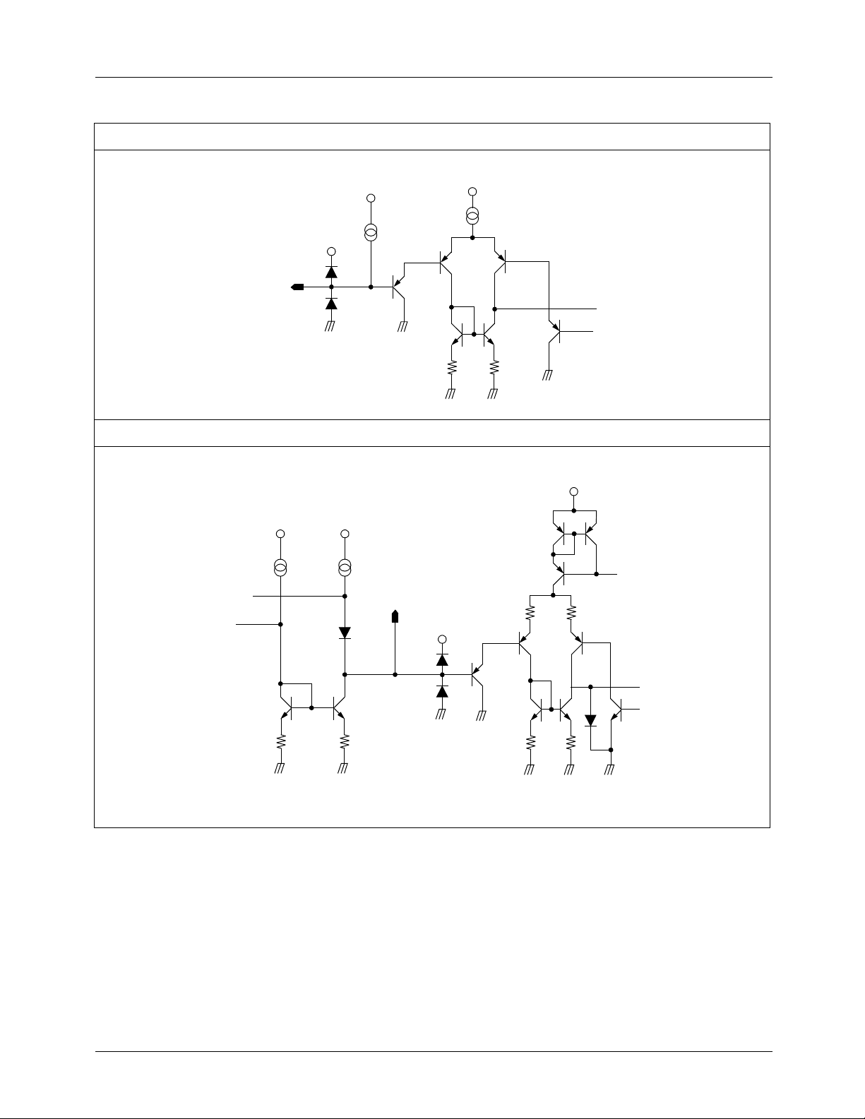
Equivalent Circuits (Continued)
KA2822D
FG zero cross output
(9Pin)
vcc
vcc
vcc
Charge pump output
vcc
vcc
vcc
to
IIL
Circuit
Charge pump
(12Pin)
vcc
Buffer amp
7
Page 8
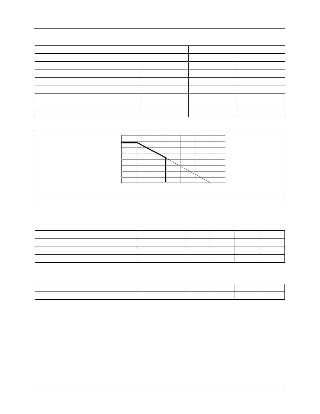
KA2822D
g
g
g
g
g
g
g
Absolute Maximum Rating (Ta=25°C)
Parameter Symbol Value Unit
Maximum power supply volta
Maximum input volta
eV
Maximum output current I
eV
CCMAX
INMAX
OMAX
Normal output current I
Power dissipation P
Operatin
temperature T
Junction temperture T
e temperature T
Stora
O
D
A
J
STG
7.0 V
0 ~ V
CC
1A
0.7 A
1.5 W
0 ~ 75
150
−
55 ~ +125
Power Dissipation Curve
2.0
V
°
C
°
C
°
C
Power
Dissipation
: PD[W]
1.5
1.0
0.5
0
0 25 50 75 100 125
Ambient temperature, Ta [°C]
150 175
Power dissipation decreases in the rate of 13.5mV / °C when mounted on 50mm × 50mm × 1mm PCB (Phen olic resin material) and used above Ta=25°C.
Recommended Operating Conditions (Ta=25°C)
Parameter Symbol Min. Typ. Max Unit
Supply volta
Supply volta
eV
e in logic part V
Ambient operatin
temperature rangeTa0-+70
CC1
, V
CC3
CC2
10.8 12.0 13.2 V
4.5 5.0 5.5 V
°
C
Temperature Characteristic
Parameter Symbol Min. Typ. Max Unit
Thermal shutdown temperature
NOTE:
Reference value
note
TSD 125 150 -
°
C
8
Page 9
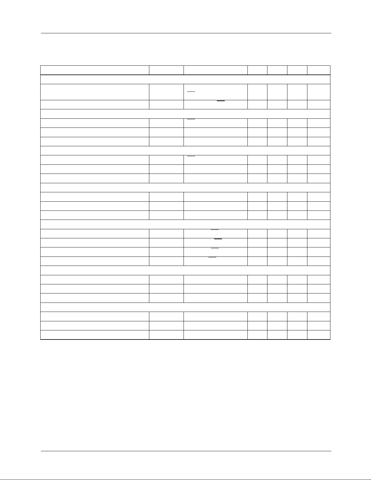
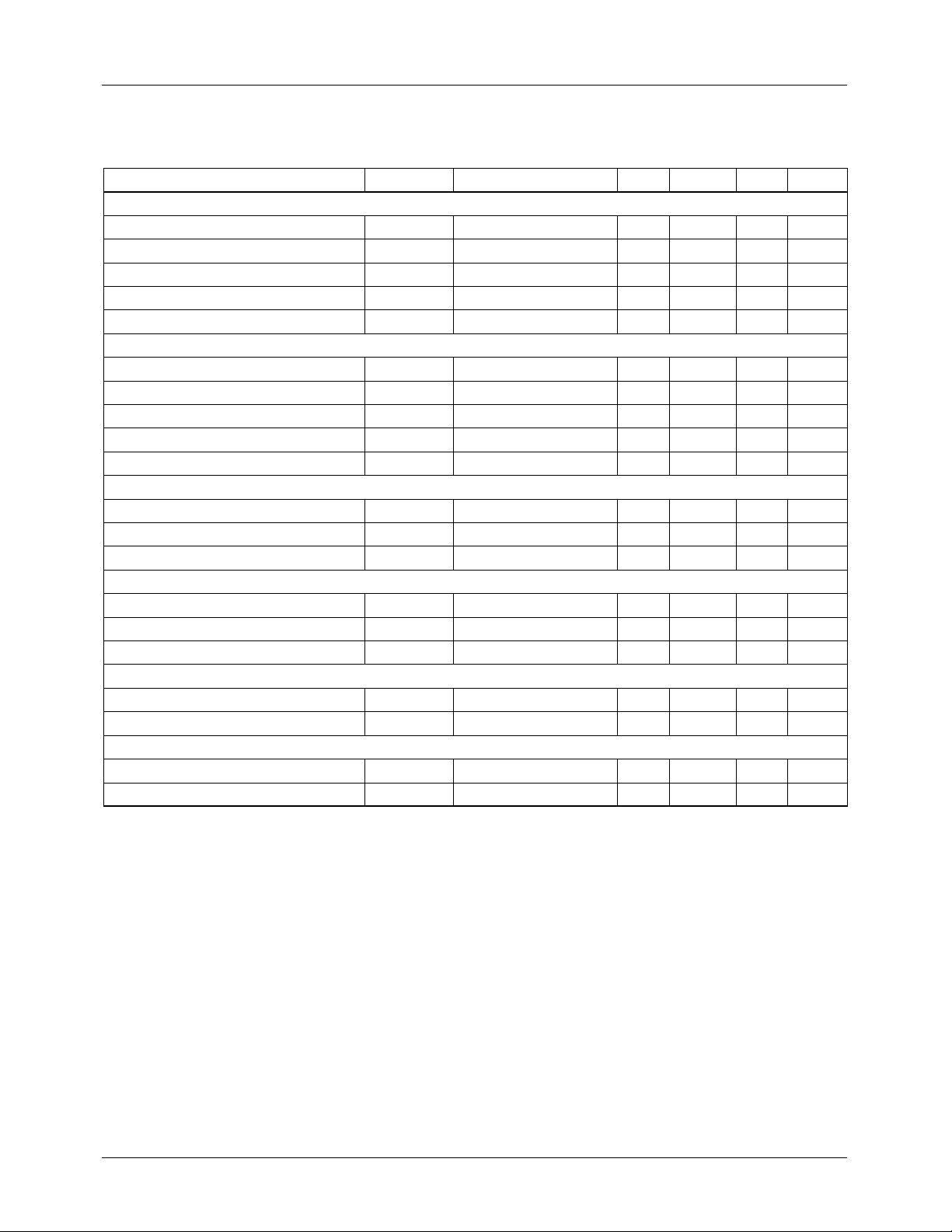
Electrical Characteristics
g
g
g
g
g
g
g
g
g
g
g
g
ge g
g
g
(Ta=25°C, VCC=5V)
Parameter Symbol Conditions Min. Typ. Max. Units
SUPPLY CURRENT
Supply current 1 I
Supply current 2 I
CHIP ENABLE
Input current I
Input low volta
Input hi
RPM SELECT
Input current I
Input low volta
Input hi
HALL AMP
Input resistance
Common mode input volta
Differential input volta
START-UP
Hall bias volta
Hall bias volta
Reference volta
Bias off current I
OUTPUT AMP
Leaka
e current I
Saturation volta
Saturation volta
BUFFER & CONTROL AMP
Volta
Reference volta
Reference volta
eI
h voltageI
eV
h voltageV
note
e range
e range
note
note
e 1 V
e 2 V
eVrefI
e 1 Vsat1 IO=0.35A - 1.0 1.2 V
e 2 Vsat2 IO=0.7A - 1.3 1.8 V
note
ain 1
note
e 1
note
e 2
KA2822D
CCO
CC
CE
CE1
CEH1
RPM
RPM1
RPMH
RI
V
COM
V
DIF
HB1
HB2
HOFF
CER
G
CT1
VCC=6.5V
=H, RPM=L
CE
VCC=6.5V, CE=L - 15 23 mA
CE=0~5V - 5 10
- - - 1.0 V
- 3.5 - - V
CE=0~5V - 5 10
- - - 1.0 V
- 3.5 - - V
N
-110-k
-2.0-V
- 100 - 420 mV
IH=4mA, CE=L 2.3 2.5 2.7 V
IH=10mA, CE=L 2.7 2.9 3.1 V
=1mA, CE=L 1.7 2.2 2.7 V
O
VH=7V, CE=H - 5 10
--0.51mA
--
- 1.0 2.0 mA
CC
−
11 - dB
Vref1 Current limiter voltage 0.205 0.208 0.210 V
Vref2 Control begin voltage - 0.69 - V
µ
A
µ
A
Ω
V
PP
µ
A
Notes:
Reference value
9
Page 10
KA2822D
g
g
g
g
ge g
g
g
g
g
g
g
g
g
g
g
Electrical Characteristics (Continued)
(Ta=25°C, VCC=5V)
Parameter Symbol Conditions Min. Typ. Max. Units
CHARGE PUMP
e current I
Char
Dischar
Current ratio
e current I
note
Off current I
note
Clamp volta
e
FG AMP
note
Output DC volta
Volta
ain 2 G
Input volta
Noise margin 1
Noise margin 2
e
e range
note
note
note
SPEED CONTROL
note
Count ran
Count ran
Operatin
e 1
note
e 2
freq. F
BURST ADJUSTMENT
Input current I
Threshold volta
Threshold volta
e 1 V
e 2 V
PULSE WIDTH ADJUSMENT
Ct2 char
Threshold volta
e current I
e 3 V
INDEX OUTPUT
Output leaka
e current
Output low volta
note
eV
CP−
CP+
I
R
OFF
V
CLP
V
FG
FG
V
IN
N
D
N
C
N1 RPM=L - 1666.5 - N2 RPM=H - 1388.5 - -
D
BI
TH1
TH2
CT2
TH3
I
OH
O1
RPM=L
−
15
RPM=L 15 20 25
I
CP+
/ I
CP−
0.9 1.0 1.1 -
−
20
−
25
µ
µ
VCP=0.63V - - 50 nA
- - 1.3 1.5 V
- 1.0 1.3 1.6 V
-243444dB
- 2.0 - 20 mV
Differential noise - - 0.5 mV
Common mode noise - - 0.5 V
P-P
- - 1.0 1.1 MHz
--12
µ
RPM=L 1.2 1.45 1.7 V
RPM=H 1.05 1.3 1.55 V
-
−
19
−
25
−
36
µ
- 0.9 1.1 1.3 V
--12
µ
IO=1mA - 0.2 0.4 V
A
A
P-P
P-P
A
A
A
Notes:
Reference value
10
Page 11

KA2822D
Application Information
1. CHIP ENABLE
This function turns on or off all blocks by low or high signal.
2. U, V AND W PHASE OUTPUT AMP
These ampilifiers drives three output phases - U, V, and W which have 120(degree) phase differences with each other. The
three phase waveforms are made with the two hall sensor signals by synthesizing the third phase signal.
3. SPEED CONTROL PART
This function compares the real motor rotation frequency with the 300 or 360Hz pulse divided from 1MHz clock pulse for
removing speed error when motor is on and speed error is detected by PLL.
The speed error sent to charge pump part which repeats charge and discharge controls the output current of the output amp to
keep a stable rotation.
11
Page 12
KA2822D
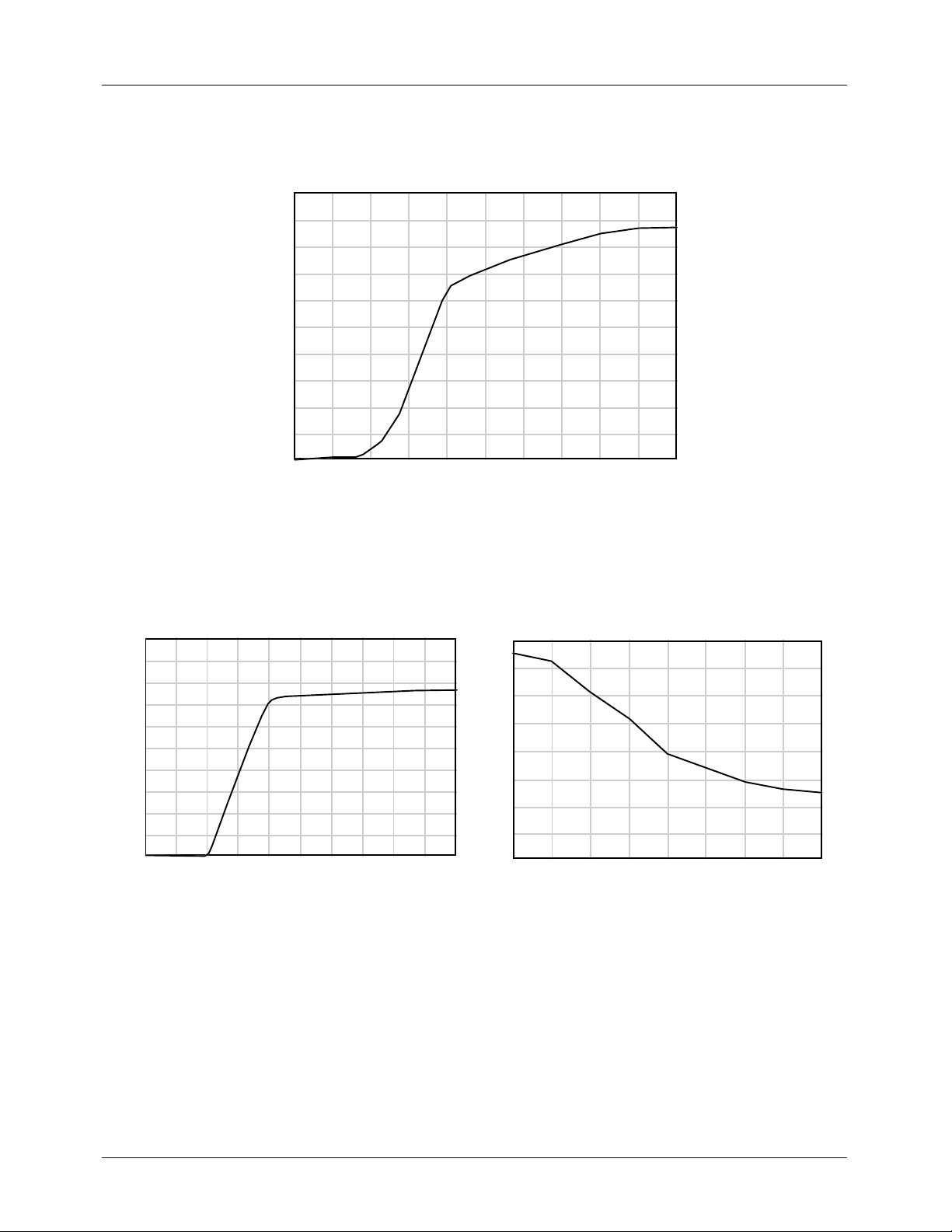
Typical Performance Cha ra cteristics
I
CC
15.0
[mA]
1.5
/div.
0
0
1. VCC vs. I
0.8/div.
V
CC
8.0[V]
CC
Vref
3.0
[V]
0.3
/div.
Index pulse width
8.0
[ms]
1.0
/div.
0
0.8/div.
V
CC
8.0[V]
0
4.2
4.5 5.0 5.5 6.0 6.5 7 .0 7.5
V
CC
8.0[V]
VCC vs. Vref (Pin4) VCC vs. Index pulse width
12
Page 13
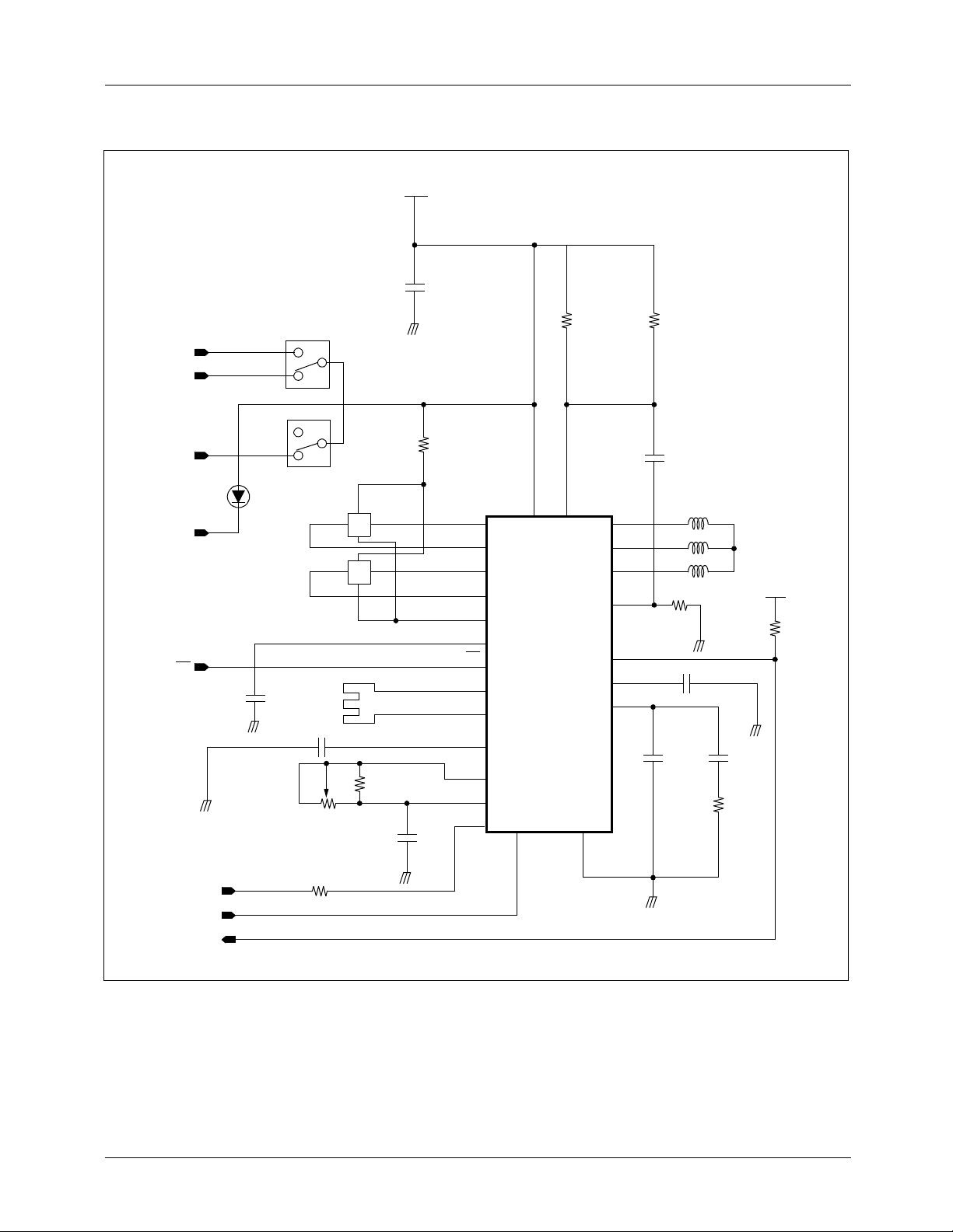
Typical Application Circuits
KA2822D
+5V
220nF
DISK_IN
W_P
H_D
LED
CE
47nF
SW1
SW2
47nF
HU
HV
56k
VOLTAGE REGULATOR
VR
100
U INPUT(+)
U INPUT(−)
U INPUT(+)
U INPUT(−)
HALL BIAS
AGC
CE
FG_INPUT(+)
FG_INPUT(-)
FG ZERO CROSS
INDEX BURST
47nF
CC
V
19
18
24
25
27
2
7
28
1
9
4
5
13 11 8
CURRENT DETECTION2
16 17
26
KA2822D
1
U PHASE OUTPUT
CURRENT DETECTION1
23
V PHASE OUTPUT
22
W PHASE OUTPUT
21
PHASE COMPENSATION
15
INDEX OUTPUT
6
OSC INPUT
3
CHARGE PUMP OUTPUT
12
1
100nF
1.8M
10nF
U
V
W
+5V
10k
100nF
100nF
330k
1MHz
RPM_SEL
INDEX
47k
13
OSC INPUT
RPM SELECT
SIGNAL GROUND
Page 14
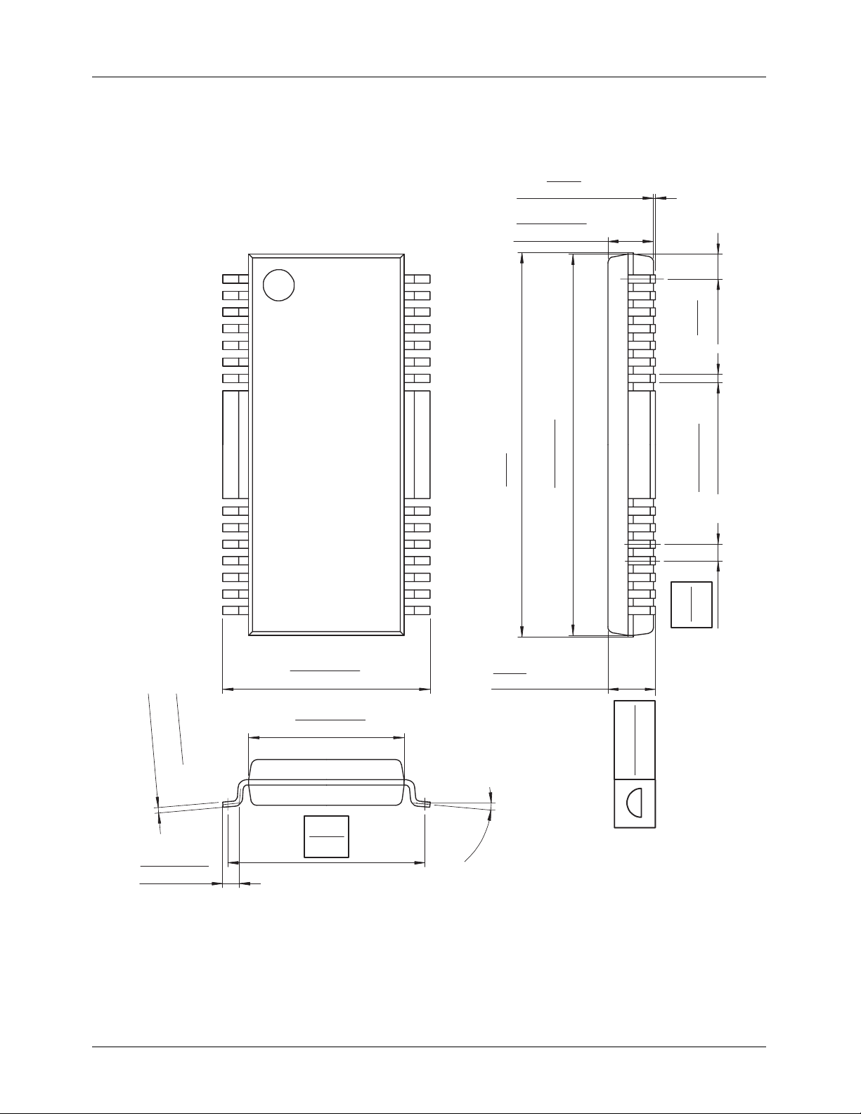
28-SSOPH-375
0.05
MIN
0.002
2.20 ±0.20
0.087 ±0.008
0.010
+
-0.002
0.004
#14
0.25
+
-0.05
0.10
#1
10.00 ±0.30
0.394 ±0.012
7.50 ±0.20
0.295 ±0.008
#28
#15
MAX
18.80
2.50
0.098
0.740
MAX
18.40 ±0.20
0.724 ±0.008
1.20
0.047
()
0.40 ±0.10
0.016 ±0.004
0.80
0.031
0.80
±0.20
0.031 ±0.008
9.53
0.375
0~8°
MAX0.10
MAX0.004
Page 15

TRADEMARKS
The following are registered and unregistered trademarks Fairchild Semiconductor owns or is authorized to use and is
not intended to be an exhaustive list of all such trademarks.
ACEx™
Bottomless™
CoolFET™
CROSSVOLT™
DOME™
E2CMOS
EnSigna
TM
TM
FACT™
FACT Quiet Series™
®
FAST
FASTr™
GlobalOptoisolator™
GTO™
HiSeC™
ISOPLANAR™
MICROWIRE™
OPTOLOGIC™
OPTOPLANAR™
POP™
PowerTrench
®
QFET™
QS™
QT Optoelectronics™
Quiet Series™
SuperSOT™-3
SuperSOT™-6
SuperSOT™-8
SyncFET™
TinyLogic™
UHC™
VCX™
DISCLAIMER
FAIRCHILD SEMICONDUCTOR RESERVES THE RIGHT TO MAKE CHANGES WITHOUT FURTHER
NOTICE TO ANY PRODUCTS HEREIN TO IMPROVE RELIABILITY, FUNCTION OR DESIGN. FAIRCHILD
DOES NOT ASSUME ANY LIABILITY ARISING OUT OF THE APPLICATION OR USE OF ANY PRODUCT
OR CIRCUIT DESCRIBED HEREIN; NEITHER DOES IT CONVEY ANY LICENSE UNDER ITS PATENT
RIGHTS, NOR THE RIGHTS OF OTHERS.
LIFE SUPPORT POLICY
FAIRCHILD’S PRODUCTS ARE NOT AUTHORIZED FOR USE AS CRITICAL COMPONENTS IN LIFE SUPPORT
DEVICES OR SYSTEMS WITHOUT THE EXPRESS WRITTEN APPROVAL OF FAIRCHILD SEMICONDUCTOR CORPORATION.
As used herein:
1. Life support devices or systems are devices or
systems which, (a) are intended for surgical implant into
the body, or (b) support or sustain life, or (c) whose
failure to perform when properly used in accordance
with instructions for use provided in the labeling, can be
reasonably expected to result in significant injury to the
user.
2. A critical component is any component of a life
support device or system whose failure to perform can
be reasonably expected to cause the failure of the life
support device or system, or to affect its safety or
effectiveness.
PRODUCT STATUS DEFINITIONS
Definition of Terms
Datasheet Identification Product Status Definition
Advance Information
Preliminary
No Identification Needed
Obsolete
Formative or
In Design
First Production
Full Production
Not In Production
This datasheet contains the design specifications for
product development. Specifications may change in
any manner without notice.
This datasheet contains preliminary data, and
supplementary data will be published at a later date.
Fairchild Semiconductor reserves the right to make
changes at any time without notice in order to improve
design.
This datasheet contains final specifications. Fairchild
Semiconductor reserves the right to make changes at
any time without notice in order to improve design.
This datasheet contains specifications on a product
that has been discontinued by Fairchild semiconductor.
The datasheet is printed for reference information only.
Rev. F1
 Loading...