

Page 1
APRIL. 1998
DATA SHEET
KA2506-01
Page 2
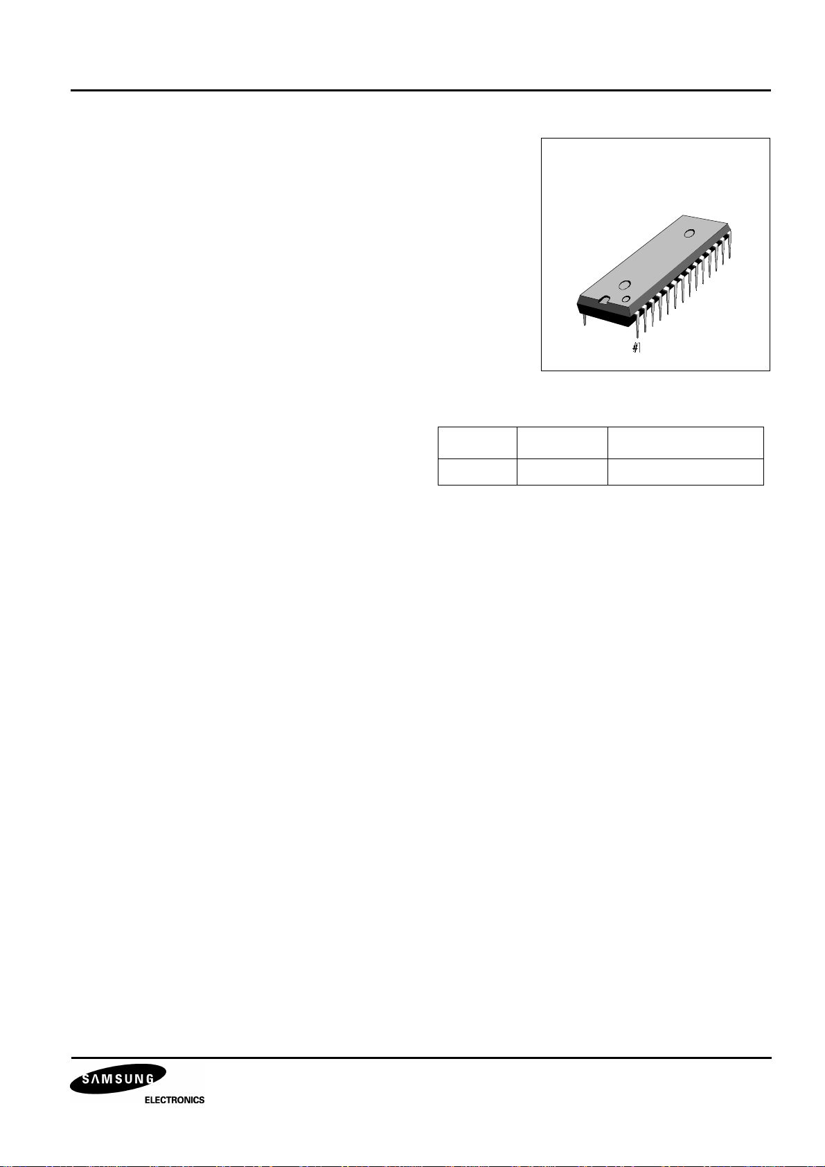
I2C BUS CONTROLLED R/G/B VIDEO AMPLIFIER FOR MONITORS KA2506-01
I2C BUS CONTROLLED R/G/B VIDEO AMPLIFIER
The KA2506-01 is a very high frequency video amplifier system with I2C Bus control used in Monitors with high resolution
up to1280 × 1024.
It contains 3 matched R/G/B video Amplifiers with OSD interface and provides flexible interfacing to I2C Bus controlled
adjustment systems.
FUNCTIONS
• R/G/B Video Amplifier
• OSD Interface
• I2C BUS Control
• Contrast/OSD Contrast
• Brightness Control
• Cut-Off Brightness Control
• R/G/B SUB Contrast/Cut-Off Control
• Blank/Clamp Gate
• Half tone (2 OSD Raster/8 Colors)
• Brightness Uniformity
ORDERING INFORMATION
28-DIP-600A
Device Package Operating Temperature
KA2506-01 28-DIP-600A -20 °C ~ +80 °C
FEATURES
• 3-Channel R/G/B Video Amplifier, 175MHz @f-3dB
• I2C Bus Control Items
- Contrast Control
- SUB Contrast Control For Each Channel
- Brightness Control
- OSD Contrast Control
- Cut-off Brightness Control
- Cut-off Control For Each Channel
- Switch Registers for SBLK and Video Half Tone and
Cut-Off INT/EXT and BPS (Blank Gate Polarity
Selection)
• SUB Contrast Control Range: -11dB
• Capable of 7.0Vpp Output Swing Range
• Video/OSD High Speed Switch
• Clamp Gate With Anti OSD Sagging
• B/U(Brightness Uniformity) Interface
• Video Input Clamp, BRT Clamp
• Video & OSD Half Tone Function on OSD
Picture (2 OSD Raster Selection by
HR1, HG1, HB1, HR2, HG2, HB2: 8 colors)
• OSD Interface, OSD BLK
• ABL
• TTL R/G/B OSD Inputs, 80MHz bandwidth
• Contrast Control Range: -38dB
• OSD Contrast Control Range: -38dB
1
Page 3
KA2506-01 I2C BUS CONTROLLED R/G/B VIDEO AMPLIFIER FOR MONITORS
CUT OFF EXT OFFSET D3:5 (0AH)
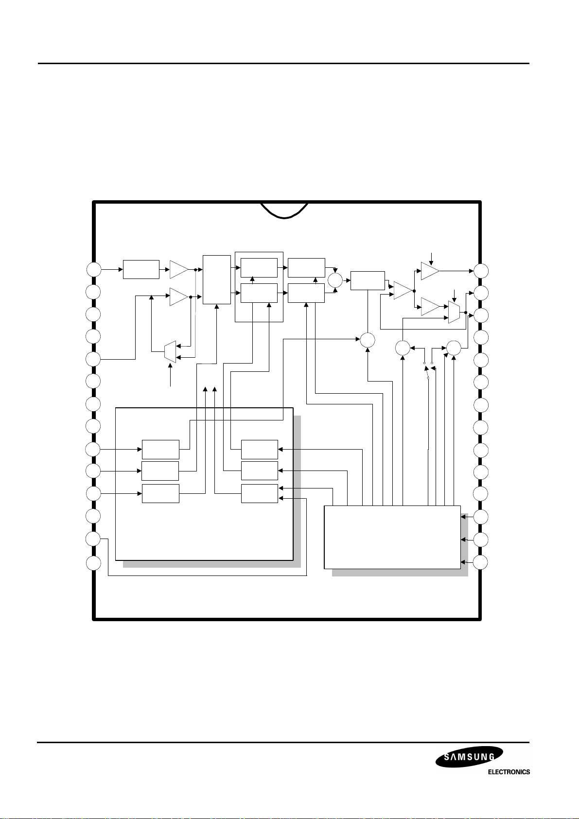
BLOCK DIAGRAM
ROSD
GOSD
BOSD
VCC2
RIN
VCC1
GND1
GIN
B/U
VI/OSD_SW
CLP
BIN
ONE (RED)
OF THREE CHANNELS
1
2
3
9
5
6
7
8
28
4
18
10
OSD
INTERFACE
gm1
CLP
B/U
INTERFACE
VIDEO/OSD
SWITCH
CLAMP
GATE
VIDEO
OSD
SWITCH
CLP BLK
OSD
RASTER
VIDEO
HALF-TONE
HALF-TONE
VIDEO
HALF-TONE
OSD RASTER
SELECT
BLANK
GATE
OSD
CONTRAST
VIDEO
CONTRAST
VIDEO-HALF TONE SWITCH
D1(0AH)
OSD RASTER COLOR
D6:7(0AH)
SOFT BLANK
D0(0AH)
BLK
ROUT
SUB
+
CONTRAST
+
R/G/B DRIVE CONTROL (02/03/04H)
CONTRAST CONTRAL (00H)
OSD CONT CONTROL (05H)
A2
A1
A3
Cut Off
+ +
R/G/B CUT OFF CONTROL (07/08/09H)
BRIGHTNESS CONTROL (01H)
CUT OFF INT/EXT SWITCH(0AH)
26
CLP
27
gm2
17
23
22
21
20
15
CUT OFF BRIGHT (06H)
24
25
16
12
RCLP
RCT
VCC3
GND3
BOUT
BCLP
BCT
GOUT
GCLP
GCT
ABL
19
BLK
INTERFACE & CONTROL
GND(L)
2
I2C BUS CONTROL
14
SDA
13
SCL11
Page 4
I2C BUS CONTROLLED R/G/B VIDEO AMPLIFIER FOR MONITORS KA2506-01
KA2506-01
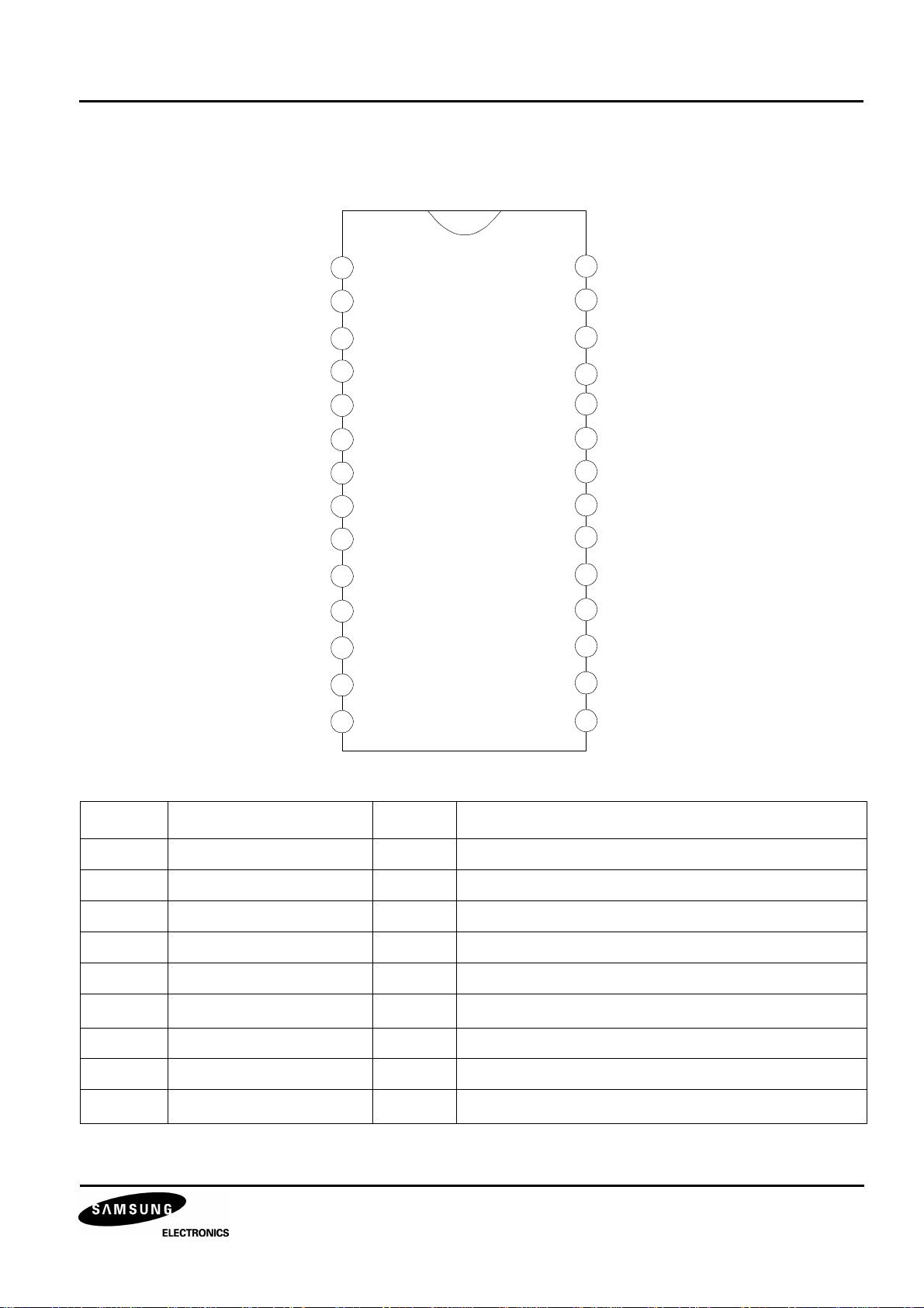
PIN CONFIGURATION
1
2
3
4
5
6
7
8
9
10
11
12
13
ROSD
GOSD
BOSD
VI/OSD_SW
RIN
VCC1
GND1
GIN
VCC2
BIN
GND(L)
ABL
SCL
B/U
RCLP
ROUT
GCLP
GOUT
VCC3
GND3
BOUT
BCLP
BLK
CLP
RCT
GCT
28
27
26
25
24
23
22
21
20
19
18
17
16
15
14
SDA
BCT
Table 1. Pin Configuration
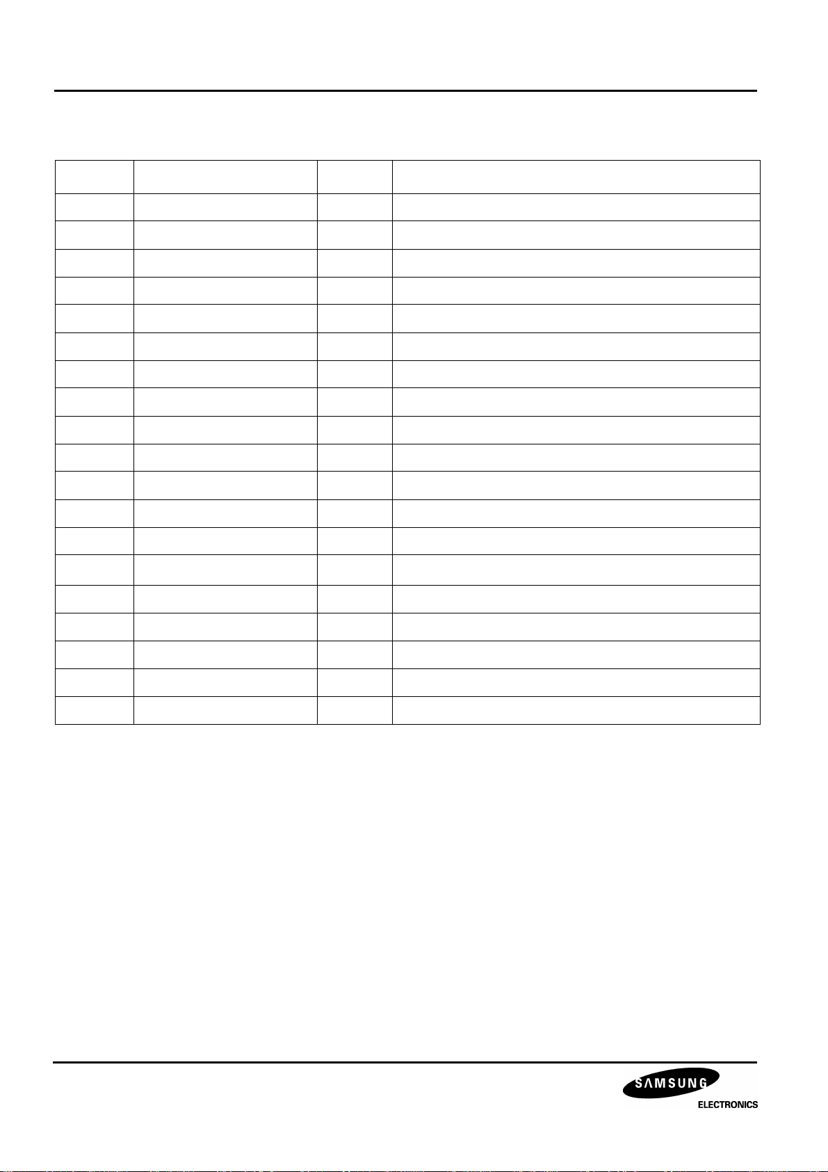
Pin No Symbol I/O Configuration
1 ROSD I Red OSD Input
2 GOSD I Green OSD Input
3 BOSD I Blue OSD Input
4 VI/OSD_SW I Video or OSD Switch
5 RIN I Red Video Input
6 V
CC1
- VCC (normal)
7 GND1 - Ground1 (normal)
8 GIN I Green Video Input
9 V
CC2
- VCC (normal)
3
Page 5
KA2506-01 I2C BUS CONTROLLED R/G/B VIDEO AMPLIFIER FOR MONITORS
Table 1. Pin Configuration
Pin No Symbol I/O Configuration
10 BIN I Blue Video Input
11 GND (L) - Ground2 (logic)
12 ABL - Automatic Beam Limit
13 SCL I/O Serial Clock
14 SDA I/O Serial Data
15 BCT I Blue Cut Off Control
16 GCT I Green Cut Off Control
17 RCT I Red Cut Off Control
18 CLP I Clamp Gate Signal Input
19 BLK I Blank Gate Signal Input
20 BCLP - Blue Clamp Cap
21 BOUT O Blue Video Output
22 GND3 - Ground3 (drive part)
23 V
CC3
- VCC (drive part)
24 GOUT O Green Video Output
25 GCLP - Green Clamp Cap
26 ROUT O Red Video Output
27 RCLP - Red Clamp Cap
28 B/U I Brightness Uniformity
4
Page 6
I2C BUS CONTROLLED R/G/B VIDEO AMPLIFIER FOR MONITORS KA2506-01
PIN DESCRIPTION
Table 2. Pin Description
Pin No Pin Name Schematic Description
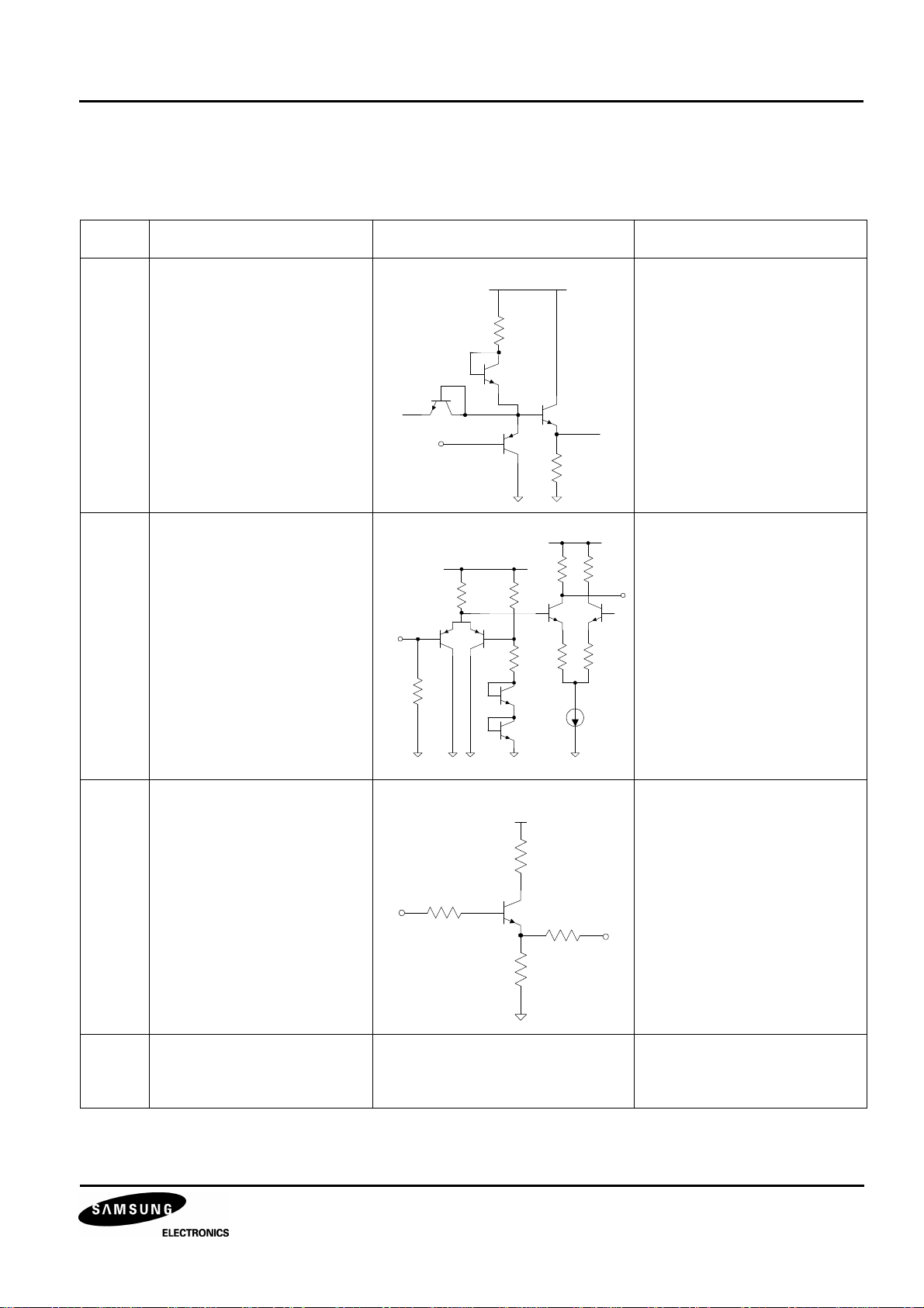
1
Red OSD Input
(ROSD)
2
Green OSD Input
(GOSD)
3
Blue OSD Input
(BOSD)
4 Video/OSD Switch
(VI/OSD_SW)
1.29/
1.02V
PIN 4
PIN 1
VCC
VCC
OSD input signals are in TTL
level and will be connected to
ground when switching to
video input
1.16/
0.90V
6V
Video/OSD switch signal is
TTL level
PIN4 = “high”, OSD input
PIN4 = “Low”, video input
5
8
10
6
9
Red Video Input
(RIN)
Green Video Input
(GIN)
Blue Video Input
(BIN)
V
CC1
V
CC2
PIN 5
VCC
MAX input video signal is
0.7 Vpp
Supply voltage
-
(except drive part)
5
Page 7
KA2506-01 I2C BUS CONTROLLED R/G/B VIDEO AMPLIFIER FOR MONITORS
Table 2. Pin Description (Continued)
Pin No Pin Name Schematic Description
7
11
15
GND1
GND2 (GND (L) )
Blue Cut-Off
(BCT)
16
Green Cut-Off
(GCT)
17
Red Cut-Off
(RCT)
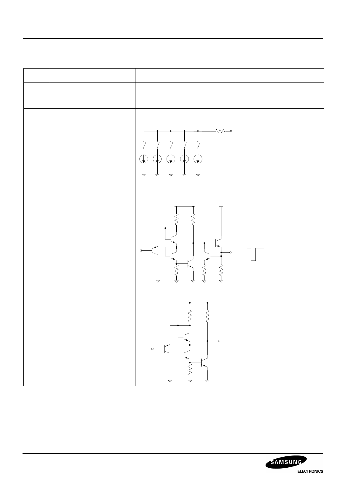
18 Clamp Gate Input
(CLP)
-
0~180uA 0~540uA 80uA 160uA 320uA
PIN 18
Cut-OffCut-Off
BRT
Cut-Off
Offset
5.1V
PIN 17
Ground (analogue)
Ground (logic)
Cut-Off Control Output
Video amp active when clamp
VCC
gate signal is in low TTL level.
Clamp gate Min. pulse width
: 0.2us, at fh: 50KHz
19 Blank Gate Input
(BLK)
PIN 19
6
7V VCC
Video amp blanks video signal
when blank gate signal is in
low TTL level.
Page 8
I2C BUS CONTROLLED R/G/B VIDEO AMPLIFIER FOR MONITORS KA2506-01
Table 2. Pin Description (Continued)
Pin No Pin Name Schematic Description
26
24
21
20
25
27
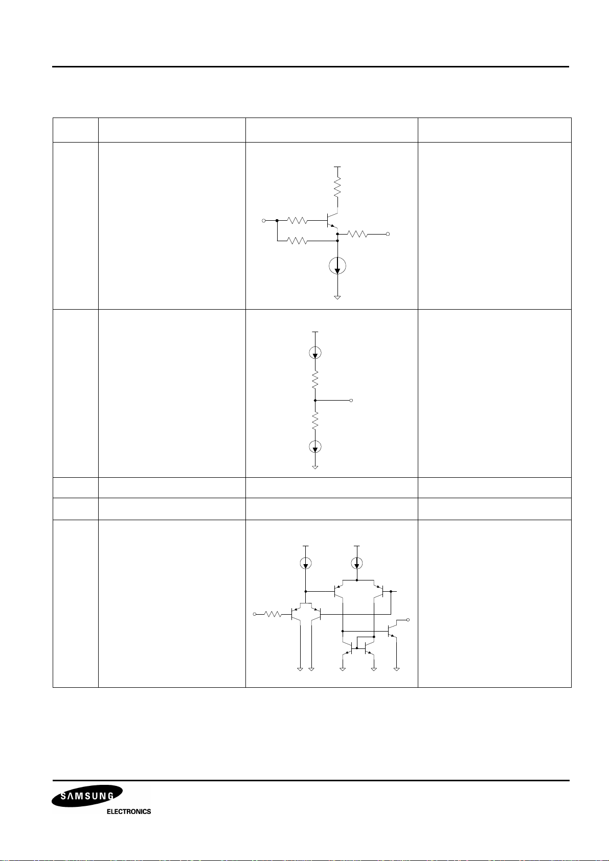
Red Video Output
(ROUT)
Green Video Output
(GOUT)
Blue Video Output
(BOUT)
Blue Clamp Cap
(BCLP)
Green Clamp Cap
(GCLP)
Red Clamp Cap
(RCLP)
VCC
Video signal output
PIN 26
Brightness control activated
by charging and discharging
of the external cap. (0.1µF)
(during low clamp gate)
PIN 27
22 GND3 - Ground (drive part)
23 V
13
14
CC3
SCL
SDA
- Supply voltage (drive part)
Serial clock input port of I2C
54uA 27uA
BUS
Serial data input port of I2C
BUS
3.22V
PIN 13
7
Page 9
KA2506-01 I2C BUS CONTROLLED R/G/B VIDEO AMPLIFIER FOR MONITORS
Table 2. Pin Description (Continued)
Pin No Pin Name Schematic Description
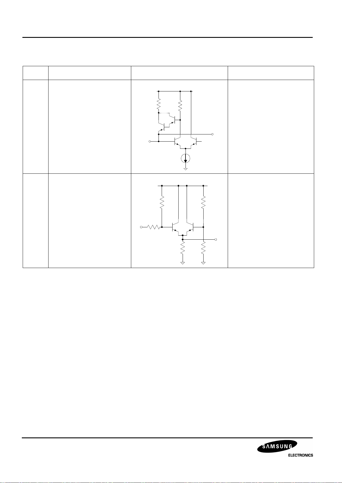
28 B/U Input (B/U) Parabola input via AC coupling
VCC
cap
PIN 28
12 ABL Input (ABL) Automatic beam limitation
4.6V
100uA
VCC
input
(control range: 0.5 ~ 4.5V)
PIN 12
8
Page 10
I2C BUS CONTROLLED R/G/B VIDEO AMPLIFIER FOR MONITORS KA2506-01
ABSOLUTE MAXIMUM RATING (TA = 25 °C)
(1)
Table 3. Absolute Maximum Rating
Value
No Item Symbol
Min Typ Max
1 Maximum Supply Voltage VCC1/2/3/V
2
Operating Temperature
(2)
Topr -20 - 80 °C
DD
- - 13.2 V
3 Storage Temperature Tstg -65 - 150 °C
4 Operating Supply Voltage Vccop 11.4 12.0 12.6
5 Power Dissipation P
D
- - 2.0 W
THERMAL & ESD PARAMETER
Table 4. Thermal & ESD Parameter
Value
No Item Symbol
Min Typ Max
Unit
(3)
V
Unit
1 Thermal Resistance
θja - 45 - °C/W
(Junction-ambient)
2 Junction Temperature Tj - 150 - °C
3 Human Body Mode
HBM 2 - - KV
(C = 100p, R = 1.5k)
4 Machine Model
MM 300 - - V
(C = 200p, R = 0)
5 Charge Device Model CDM 800 - - V
ELECTRICAL CHARACTERISTICS
DC Electrical Characteristics
Ta = 25 °C, V
Supply Current
Clamp Gate Low Input Voltage V
CC1
= V
CC2
= V
= 12V; V4 = 0V; unless otherwise stated
CC3
Table 5. DC Electrical Characteristics
Parameter Symbol Min Typ Max Unit
I
CC
(4)
151
85 110 122 mA
0.8 1.5 3.0 V
Clamp Gate High Input Voltage V
15h
0.8 1.5 2.0 V
9
Page 11
KA2506-01 I2C BUS CONTROLLED R/G/B VIDEO AMPLIFIER FOR MONITORS
Table 5. DC Electrical Characteristics (Continued)
Parameter Symbol Min Typ Max Unit
Clamp Gate Low Input Current I
Clamp Gate High Input Current I
Blank Gate Low Input Voltage V
Blank Gate High Input Voltage V
Blank Gate Low Input Current I
Blank Gate High Input Current I
15l
15h
16l
16h
16l
16h
-5.0 -2.0 - µA
- 0.01 1.0 µA
0.8 1.5 3.0 V
0.8 1.5 2.0 V
-5.0 -2.0 - µA
- 0.01 1.0 µA
Video Input bias Voltage Vbias 1.6 1.9 2.2 V
Output Clamp Cap Charge Current Iclamp+ 0.45 0.75 1.10 mA
Output Clamp Cap Discharge Current Iclamp- -1.10 -0.75 -0.45 mA
Video Output Low Voltage V
Video Output High Voltage V
Video Black Level Output Voltage V
Video ∆Black Level Output Voltage
∆VO
Video Output Blanked Voltage V
OL
OH
OBL
BL
OB
(5)
- 100 200 mV
6.2 7.5 9.0 V
0.9 1.2 1.5 V
-0.3 - 0.3 V
- 0.1 0.2 V
Contrast/Drive Control Input Current losd, ldirve
- 0.25 1 uA
lcon
Spot Killer Voltage Vspot 9.2 10.4 11.2 V
10
Page 12
I2C BUS CONTROLLED R/G/B VIDEO AMPLIFIER FOR MONITORS KA2506-01
AC Electrical Characteristics
Ta = 25 °C, V
Vin = 0.56Vpp Manually adjust Video Output pins 21, 24 and 26 to 4V DC for the AC test
(12)
stated
CC1
= V
CC2
= V
= 12V; V4 = 0V.
CC3
(11)
unless otherwise
Table 6. AC Electrical Characteristics
Parameter Symbol Min Typ Max Unit
Video Amplifier Gain AV max 15.5 17.5 19.5 dB
Contrast Attenuation 1 Avc1 -4.5 -6.0 -7.5 dB
Contrast Attenuation 2 Avc2 - -38 -35 dB
Drive Attenuation1 Avd1 -3 -4 -5 dB
Drive Attenuation 2 Avd2 -11 -8 -5 dB
(7)
(6)
-1 - 1 dB
-1 - 1 dB
Absolute Gain Match
Gain Change between Amplifiers
AV match
AV track
Video Amplifier Distortion THD - 1 5 %
Video Amp Bandwidth
(7,8)
Video Output Rise Time
(7)
f (-3dB) 150 175 - MHz
tr (Video) - 2.0 2.3 ns
Video Output Fall Time
(7)
Video Amplifier 10kHz Isolation
Video Amplifier 10MHz Isolation
Blank Output Rise Time
Blank Output Fall Time
(7)
(7)
tf (Video) - 2.5 2.8 ns
Viso_10K
Viso_10M
(9)
(7,9)
- -65 -45 dB
- -50 -35 dB
tr (Blank) - 6 15 ns
tf (Blank) - 10 30 ns
End of Blanking Propagation Delay tr-prop (Blank) - 23 50 ns
Start of Blanking Propagation Delay tf-prop (Blank) - 20 45 ns
OSD Electrical Characteristics
Ta = 25 °C, V
CC1
= V
CC2
= V
= 12V; V19 = 4V; V12 = V28 = 0V;
CC3
V1 = V2 = V3 = 4V; V4 = 4V; unless otherwise stated
Table 7. OSD Electrical Characteristics
Parameter Symbol Min Typ Max Unit
OSD Input Low Input Voltage V
OSDI
0.4 1.3 3.0 V
11
Page 13
KA2506-01 I2C BUS CONTROLLED R/G/B VIDEO AMPLIFIER FOR MONITORS
Table 7. OSD Electrical Characteristics (Continued)
Parameter Symbol Min Typ Max Unit
OSD Input High Input Voltage V
OSD Select Low Input Voltage V
OSD Select High Input Voltage V
OSD Select Low Input Current I
OSD Select High Input Current I
OSD Output Black Level V
BLV-OSD
OSD Output Voltage V
OSD Output Vpp Attenuation V
OSD Intensity Attenuation V
OSD_ATT
INT_ATT
Output Match between Channels V
Video to OSD Switch Time
OSD to Video Switch Time
(7)
(7)
tr (OSD S) - 4 10 ns
tf (OSD S) - 11 20 ns
OSDh
4I
4h
4I
4h
OSD
OSD
0.4 0.8 1.2 V
0.8 1.6 3.0 V
0.8 1.6 2.0 V
-10 -5 - µA
70 100 130 µA
- 0.1 0.2 V
2.6 3.6 4.6 V
30 50 70 %
30 50 70 %
-7 - 7 %
Video to OSD Propagation Delay tr-pr (OSD S) - 11 25 ns
OSD to Video Propagation Delay tf-pr (OSD S) - 12 25 ns
PP
OSD Rising Time tr (OSD) - 4 8 ns
OSD Falling Time tf (OSD) - 5 10 ns
OSD Rising Propagation Delay tr_pr (OSD) - 7 15 ns
OSD Falling Propagation Delay tf_pr (OSD) - 9 20 ns
Video/OSD 10kHz Isolation Iiso10K (OSD) - -60 -40 dB
Video/OSD 10MHz Isolation Iiso10M (OSD) - -50 -35 dB
12
Page 14
I2C BUS CONTROLLED R/G/B VIDEO AMPLIFIER FOR MONITORS KA2506-01
I2C BUS Recommended Operating Conditions
Table 8. I2C BUS Recommended Operating Conditions
Parameter Symbol Min Typ Max Unit
Input High Level Voltage VinH 3.0 - - V
Input Low Level Voltage VinL - - 1.5 V
SCL Clock Frequency f
Hold Time Before a new transmission can start t
Hold Time for Start Condition t
Set-up Time for Stop Conditions t
The Low Period of SCL t
The High Period of SCL t
Hold Time Data t
Set-up Time Data t
Rise Time of SCL t
Fall Time of SCL t
I2C BUS Timing Requirement
SCL
BUF
HDS
SUP
LOW
HIGH
HDAT
SUPDAT
R
F
- - 200 kHz
1.3 - - uS
0.6 - - uS
0.6 - - uS
1.3 - - uS
0.6 - - uS
0.3 - - uS
0.25 - - uS
- - 1.0 uS
- - 3.0 uS
SDA
SCL
t
BUF
t
HDS
t
HDAT
t
SUPDAT
t
HIGH
t
LOW
t
SUP
13
Page 15
KA2506-01 I2C BUS CONTROLLED R/G/B VIDEO AMPLIFIER FOR MONITORS
NOTES;
1. Absolute Maximum Rating Indicates the limit beyond which damage to the device may occur.
2. Operating Ratings indicate conditions for which the device is functional but do not guarantee specific performance limits.
For guaranteed specifications and test conditions, See the Electrical Characteristics. The guaranteed specifications apply
only for the test conditions listed. Some performance characteristics may degrade when the device is not operated under
the listed test conditions.
3. VCC supply pins 6, 9, and 23 must be externally wired together to prevent internal damage during VCC power on/off
cycles.
4. The supply current specified is the quiescent current for V
for V
5. Output voltage is dependent on load resistor. Test circuit uses RL = 390Ω
6. Measure gain difference between any two amplifiers Vin = 560mVpp.
7. When measuring video amplifier bandwidth or pulse rise and fall times, a double sided full ground plane printed circuit
board without socket is recommended. Video amplifier 10MHz isolation test also requires this printed circuit board.
The reason for a double sided full ground plane PCB is that large measurement variations occur in single sided PCBs.
8. Adjust input frequency from 10MHz (AV max reference level) to the-3dB frequency (f -3dB).
9. Measure output levels of the other two undriven amplifiers relative to the driven amplifier to determine channel separation.
Terminate the undriven amplifier inputs to simulate generator loading. Repeat test at fin = 10MHz for Iso_10MHz.
10. A minimum pulse width of 200 ns is guaranteed for a horizontal line of 15kHz. This limit is guaranteed by design. if a lower
line rate is used a longer clamp pulse may be required.
11. During the AC test the 4V DC level is the center voltage of the AC output signal. For example. if the output is 4Vpp the
signal will swing between 2V DC and 6V DC.
12. These parameters are not tested on each product which is controlled by an internal qualification procedure.
(pin 23) also depends on the output load.
CC3
CC1/VCC2
and V
with RL =
CC3
∞ .
The supply current
14
Page 16
I2C BUS CONTROLLED R/G/B VIDEO AMPLIFIER FOR MONITORS KA2506-01
FUNCTIONAL DESCRIPTION
Contrast (OSD Contrast Adjustment) (8-bits)
The contrast adjustment is made by controlling simultaneously the gain of three internal variable gain amplifiers
through the I2C bus interface.
The contrast adjustment allows you to cover a typical range of 38dB.
Brightness Adjustment (8-bits)
The brightness adjustment controls to add the same black level (pedestal) to the 3-channel/R/G/B signals after
contrast amplifier by I2C BUS.
Cut-Off Brightness Adjustments (8-bits)
The Cut-Off Brightness adjustment is made by simultaneously controlling the external cut-off current.
Cut-Off(SUB Contrast) Adjustment (8-bits × 3)
These adjustments are used to adjust the white balance, and the gain of each channel is controlled by I2C BUS.
The SUB contrast adjustment allows you to cover a typical range of 11dB.
OSD Inputs
The KA2506 includes all the circuitry necessary to mix OSD signals into the R/G/B video signal.
You need 4 pins for this function. (R/G/B OSD, OSD blanking)
Serial Interface
The 2-wires serial interface is an I2C BUS interface.
The slave address of the KA2506 is DC (hexadecimal)
Bit8 Bit7 Bit6 Bit5 Bit4 Bit3 Bit2 Bit1
1 1 0 1 1 1 0 0 (W)
Data Transfer
All bytes are sent MSB (Most Significant Bit) bit first and the write data transfer is closed by a stop.
The MCU can write data into the KA2506 registers. To do that, after a start, the MCU must send:
- The I2C address slave byte with a low level for R/W bit (bit1)
- The byte of the interinal register address where the MCU wants to write data (SUB Address)
- The data
- Stop
I2C BUS Write Operation
MSB LSB
SCL
transter
SDA
START Slave address ACK Register address ACK Data byte ACK STOP
15
Page 17
KA2506-01 I2C BUS CONTROLLED R/G/B VIDEO AMPLIFIER FOR MONITORS
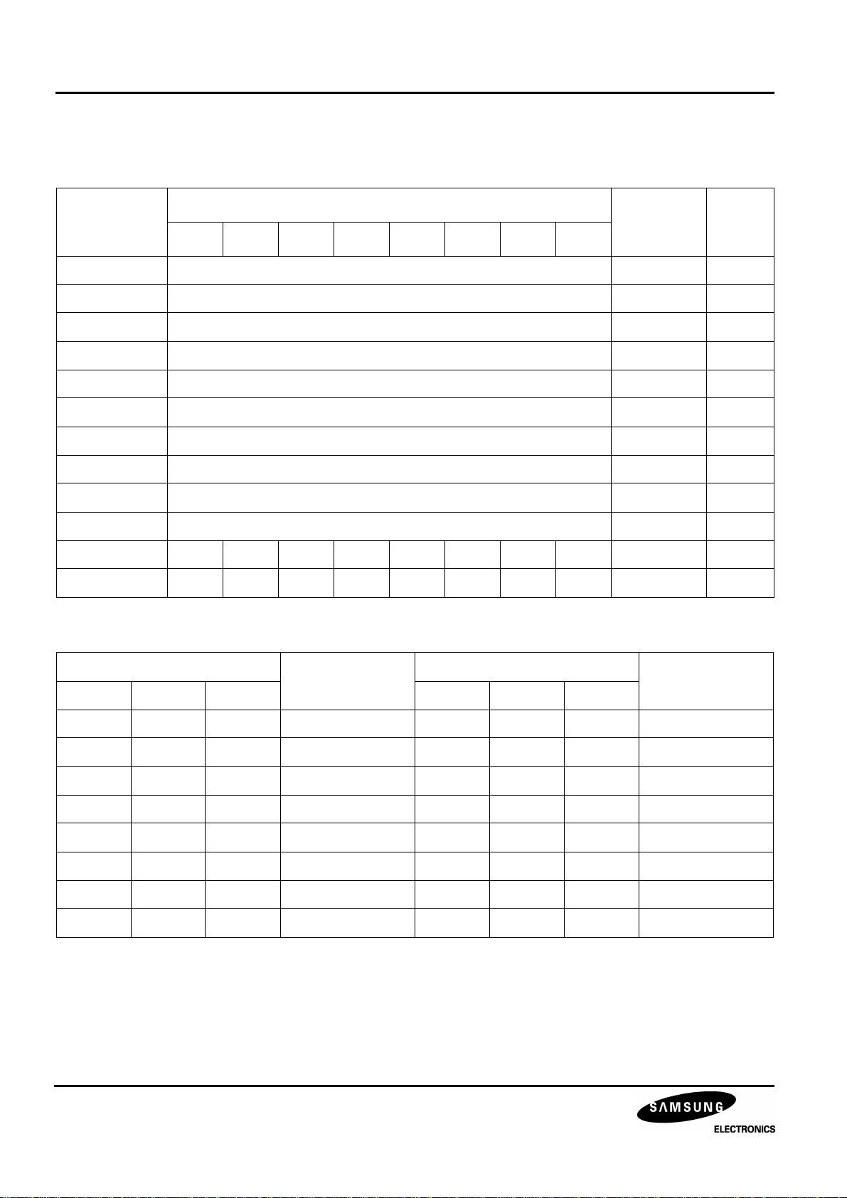
Register Description
Register Sub Address (Slave address: DCH)
Sub Address
(Hex)
00 Contrast control 80 8 bit
01 Brightness control (3-ch) 40 8 bit
02 SUB Contrast control (R) 80 8 bit
03 SUB Contrast control (G) 80 8 bit
04 SUB Contrast control (B) 80 8 bit
05 OSD Contrast control 80 8 bit
06 Cut-off Brightness control 80 8 bit
07 Cut-off control (R) 80 8 bit
08 Cut-off control (G) 80 8 bit
09 Cut-off control (B) 80 8 bit
0A - HT HR2 HG2 HB2 HR1 HG1 HB1 00 0B - - CS3 CS2 CS1 CT BPS SBLK 00 -
HT: Video Half Tone ctrl switch (1: ON, 0: OFF)
D7 D6 D5 D4 D3 D2 D1 D0
Function
Int. value
(Hex)
DAC
bits
HR/HG/HB: OSD Raster Color Switch for Video&OSD Half Tone
OSD Raster1
HR1 HG1 HB1 HR2 HG2 HB2
0 0 0 Black (Int.) 0 0 0 Black (Int.)
0 0 1 Blue 0 0 1 Blue
0 1 0 Green 0 1 0 Green
0 1 1 Cyan 0 1 1 Cyan
1 0 0 Red 1 0 0 Red
1 0 1 Magenta 1 0 1 Magenta
1 1 0 Yellow 1 1 0 Yellow
1 1 1 White 1 1 1 White
CT: Cut-off Control INT/EXT (0: INT/1: EXT) select switch (DC/AC mode)
CS1/CS2/CS3/: 80/160/320uA Cut-Off ctrl EXT offset current switch (CT = 1)
SBLK: Soft Blanking switch (1: ON, 0: OFF)
BPS: Blanking Input Polarity Selection(1: Pos, 0: Neg)
Half Tone
OSD Raster2
Half Tone
16
Page 18
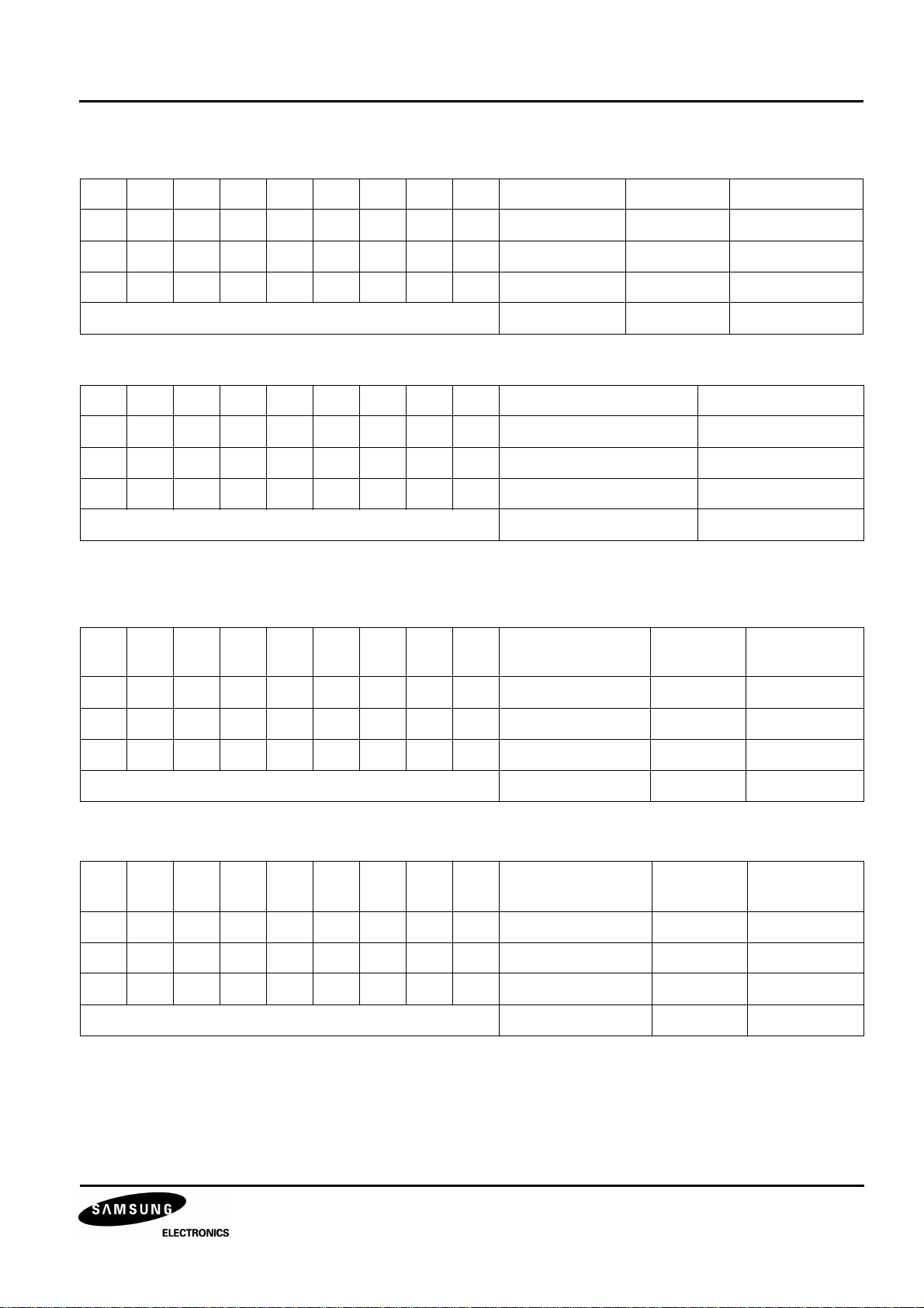
I2C BUS CONTROLLED R/G/B VIDEO AMPLIFIER FOR MONITORS KA2506-01
Contrast Register (SUB ADRS: 00H) (Vin = 0.56Vpp, bright: 40H, subcont: FFH)
Hex B7 B6 B5 B4 B3 B2 B1 B0 Contrast (Vpp) Gain (dB) Int. value (Hex)
00 0 0 0 0 0 0 0 0 0 -30.0
80 1 0 0 0 0 0 0 0 1.12 11.5 O
FF 1 1 1 1 1 1 1 1 4.2 17.5
Increment/bit 0.0164
Brightness Register (3-ch) (SUB ADRS: 01H) (cont: 40H, subcont: FFH)
Hex B7 B6 B5 B4 B3 B2 B1 B0 Brightness (Vpp) Int. value (Hex)
00 0 0 0 0 0 0 0 0 0
40 0 1 0 0 0 0 0 0 1 O
FF 1 1 1 1 1 1 1 1 4
Increment/bit 0.0156
SUB Contrast Register (R/G/B-ch) (SUB ADRS: 02/03/04H)
(Vin=0.56Vpp, bright: 40H, cont: FFH)
Hex B7 B6 B5 B4 B3 B2 B1 B0 SUB Contrast
(Vpp)
00 0 0 0 0 0 0 0 0 1.33 7.5
80 1 0 0 0 0 0 0 0 2.65 13.5 O
FF 1 1 1 1 1 1 1 1 4.2 17.5
Increment/bit 0.0123
OSD Contrast Register (SUB ADRS: 05H) (VOSD = TTL, bright: 40H, subcont: FFH)
Hex B7 B6 B5 B4 B3 B2 B1 B0 OSD Contrast
(Vpp)
00 0 0 0 0 0 0 0 0 0 80 1 0 0 0 0 0 0 0 3.7 - O
FF 1 1 1 1 1 1 1 1 3.5 -
Increment/bit 0.0289
Gain
(dB)
Gain
(dB)
Int. value
(Hex)
Int. value
(Hex)
17
Page 19
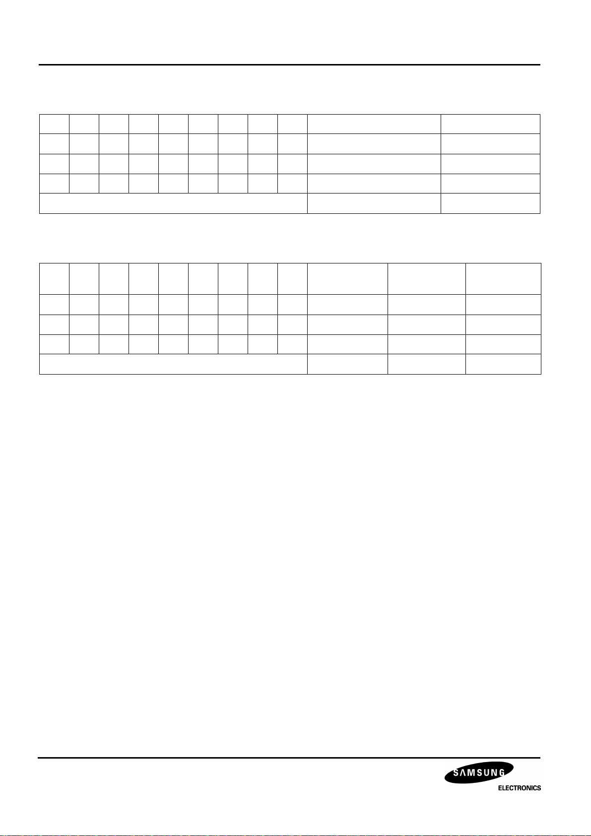
KA2506-01 I2C BUS CONTROLLED R/G/B VIDEO AMPLIFIER FOR MONITORS
Cut-Off Brightness Register (3-ch) (SUB ADRS: 06H)
Hex B7 B6 B5 B4 B3 B2 B1 B0 Cut-Off Brightness (µA) Int. value (Hex)
00 0 0 0 0 0 0 0 0 0
80 1 0 0 0 0 0 0 0 75 O
FF 1 1 1 1 1 1 1 1 150
Increment/bit 0.588
Cut-Off Register (R/G/B-ch) (SUB ADRS: 07/08/09H)
(cont = 80H, subcont: FFH, INT: CT=0, EXT: CT=1)
Hex B7 B6 B5 B4 B3 B2 B1 B0 Cut-Off INT (V) Cut-Off
EXT(µA)
00 0 0 0 0 0 0 0 0 -0.5 0
80 1 0 0 0 0 0 0 0 0 250 O
FF 1 1 1 1 1 1 1 1 0.5 500
Increment/bit 3.9mV 1.96
Int. value
(Hex)
18
Page 20
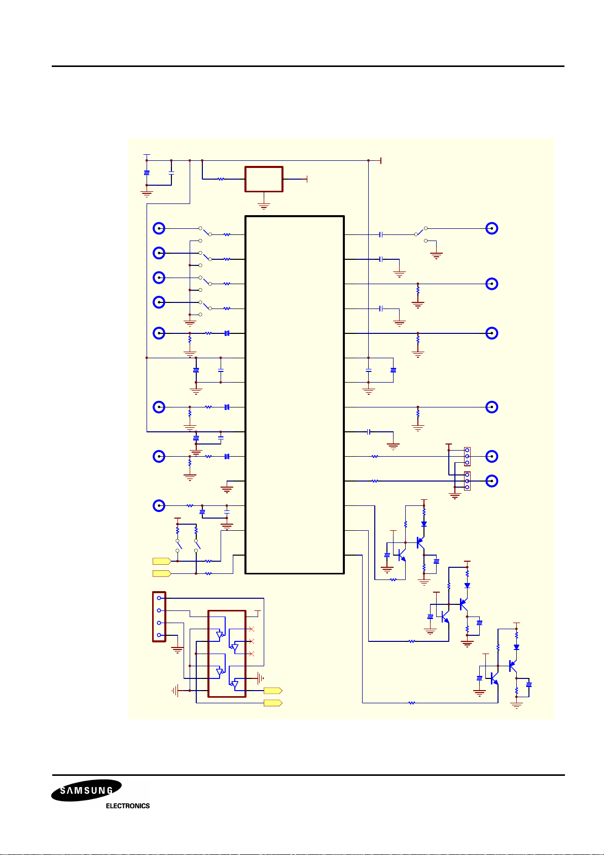
I2C BUS CONTROLLED R/G/B VIDEO AMPLIFIER FOR MONITORS KA2506-01
APPLICATION BOARD CIRCUIT
VCC=12V
+
100uF 0.1uF
ROSD In
GOSD In
BOSD In
VI/OSD SW In
Red In
Green In
Blue In
ABL In
5V
2K
SCL
SDA
1
SCLK
2
SDAT
3
ACK
4
100
75
75
75
+
100uF
+
100uF
2K
1
2
3
4
5
6
7
33
33
33
+
47uF
100
100
74HCT125
100
33
33
33
33
10uF
0.1uF
10uF
0.1uF
10uF
+
+
+
1
1
2
3
4
5
6
7
8
9
10
11
12
0.1uF
13
14
KA78T05
Vin
Vout
GND
2
ROSD
GOSD
BOSD
VI/OSD_SW
RIN
VCC1
GND1
GIN
VCC2
BIN
GND(L)
ABL
SCL
SDA
5V
14
13
12
11
10
9
8
SCL
SDA
3
KA2506-01
12V
5V
BU In
0.1uF
28
B/U
0.1uF
27
RCLP
75V
KSP92
1uF
100V
75K
BAV21
2.2K
Red Out
Green Out
Blue Out
BLK In
CLP In
+
0.47uF
50V
12V
+
75K
KSP42
75V
KSP92
75K
BAV21
2.2K
+
50V
0.47uF
ROUT
GCLP
GOUT
VCC3
GND3
BOUT
BCLP
BLK
CLP
RCT
GCT
BCT
26
0.1uF
25
24
23
0.1uF
22
21
0.1uF
20
100
19
100
18
17
16
15
1uF
100V
12V
+
100
+
100uF
75K
KSP42
100
100
390
390
390
75V
1uF
100V
75K
BAV21
KSP92
2.2K
12V
+
+
0.47uF
50V
5V
75K
KSP42
19
Page 21
KA2506-01 I2C BUS CONTROLLED R/G/B VIDEO AMPLIFIER FOR MONITORS
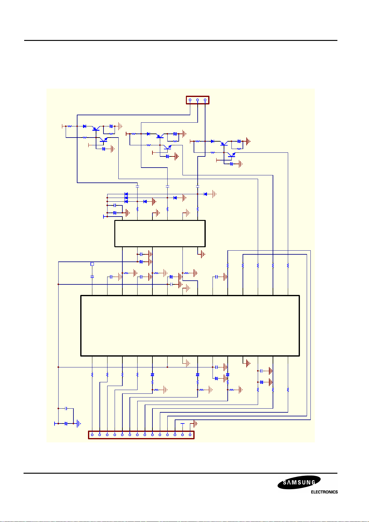
APPLICATION CIRCUIT
75V
75K
BAV21
75K
12V
BU
To Cathode
0.47uF
50V
+
KSP92
2.2K
KSP42
75V
+
1uF
100V
0.1uF
100uF
+
75V
VCC
RIN
390
0.1uF
0.1uF
28
26
27
75K
0.1uF
27
25
ROUT
VEE
0.1uF
100uF
+
0.1uF
BAV21
75K
12V
GND
GIN
24
390
KSP92
27 0.1uF
KSP42
+
1uF
GOUT
100uF
+
0.1uF
23
+
2.2K
100V
0.47uF
50V
GND
BIN
390
R Out
75V
G Out
0.1uF
27
21
75K
GND BOUT
B Out
BAV21
75K
20
12V
0.1uF
KSP92
100
19
KSP42
+
1uF
+
2.2K
100V
0.47uF
50V
100
18
100
100
100
17
15
16
B/U
RCLP
ROUT
GCLP
GOUT
VCC3
ROSD1GOSD2BOSD3VI/OSD_SW4RIN5VCC16GND17GIN8VCC29BIN10GND(L)11ABL
33
B In
ABL
33
+
SCL
10uF
75
SDA
CLP
BLK
VCC=12V
+
100uF 0.1uF
33
R OSD
G OSD
33
B OSD
33
R In
OSD SW
G In
20
GND322BOUT
KA2506-01
10uF
12V
CLP
BLK
BCLP
+
33
75
+
+
100uF 0.1uF
10uF75
33
100
RCT
12
47uF 0.1uF
+
100
13
GCT
SCL
BCT
SDA
14
100
Page 22
I2C BUS CONTROLLED R/G/B VIDEO AMPLIFIER FOR MONITORS KA2506-01
Vout [V]
18mV/Bit
Iout [uA]
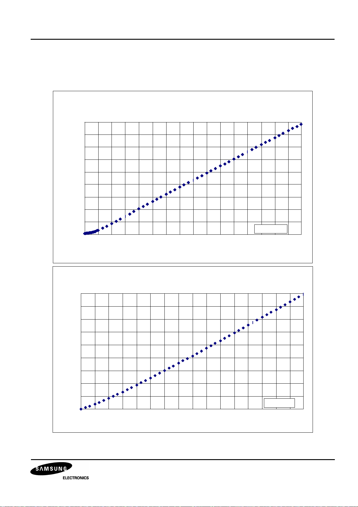
CHARACTERISTICS CURVE
Brightness (01H)
Cut-Off (07/08/09H): 80H
4.5
4.0
3.5
3.0
2.5
2.0
1.5
1.0
0.5
0.0
180
160
140
120
100
80
60
40
0 10 20 30 40 50 60 70 80 90 A0 B0 C0 D0 E0 F0
Data
Cut-Off Brightness Control (06H)
SW (0AH): 04H
20
0.7uA/Bit
0
0 10 20 30 40 50 60 70 80 90 A0 B0 C0 D0 E0 F0
Data
21
Page 23
KA2506-01 I2C BUS CONTROLLED R/G/B VIDEO AMPLIFIER FOR MONITORS
Vout [V]
Iout [uA]
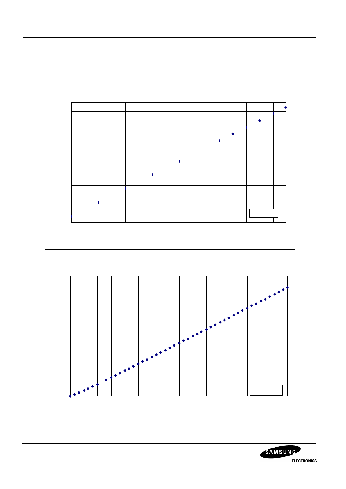
Cut-Off BRT (06H): 00H
Int. Cut-Off Control (07/08/09H)
Bright (01H): 80H
2.7
2.5
2.3
2.1
1.9
1.7
1.5
0 10 20 30 40 50 60 70 80 90 A0 B0 C0 D0 E0 F0
Ext. Cut-Off Control (07/08/09H)
600
500
400
300
200
4.6mV/Bit
Data
100
0
0 10 20 30 40 50 60 70 80 90 A0 B0 C0 D0 E0 F0
22
2.14uA/Bit
Data
Page 24
I2C BUS CONTROLLED R/G/B VIDEO AMPLIFIER FOR MONITORS KA2506-01
Vout [dB]
Vout [Vpp]
Contrast Control (00H)
4.5
Vin = 560mVpp
4
3.5
3
2.5
2
1.5
1
0.5
18.36mVpp/Bit
0
0 10 20 30 40 50 60 70 80 90 A0 B0 C0 D0 E0 F0
Contrast Control (00H)
Drive (02/03/04H): FFH
20
Data
10
0
-10
-20
-30
-40
-50
0 10 20 30 40 50 60 70 80 90 A0 B0 C0 D0 E0 F0
Data
23
Page 25
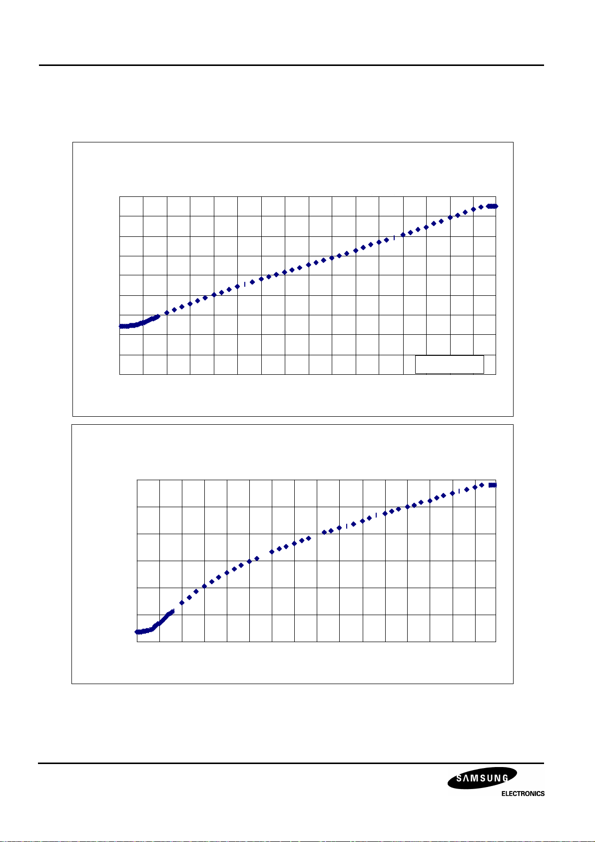
KA2506-01 I2C BUS CONTROLLED R/G/B VIDEO AMPLIFIER FOR MONITORS
Vout [Vpp]
Vout [Vpp]
Drive Control (02/03/04H)
Vin = 560mVpp
4.5
4
3.5
3
2.5
2
1.5
1
0.5
12mVpp/Bit
0
0 10 20 30 40 50 60 70 80 90 A0 B0 C0 D0 E0 F0
Drive Control (02/03/04H)
Contrast(00H): FFH
18.00
16.00
14.00
12.00
10.00
8.00
6.00
0 10 20 30 40 50 60 70 80 90 A0 B0 C0 D0 E0 F0
Data
Data
24
Page 26
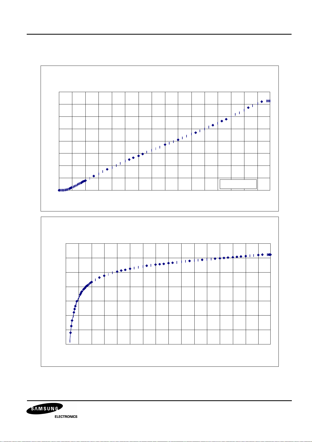
I2C BUS CONTROLLED R/G/B VIDEO AMPLIFIER FOR MONITORS KA2506-01
Vout [dB]
Vout [Vpp]
OSD Contrast Control (05H)
Drive (02/03/04H): FFH
8
7
6
5
4
3
2
1
28.6mVpp/Bit
0
0 10 20 30 40 50 60 70 80 90 A0 B0 C0 D0 E0 F0
OSD Contrast Control (05H)
Drive (02/03/04H): FFH
30
20
10
0
-10
-20
-30
Data
-40
0 10 20 30 40 50 60 70 80 90 A0 B0 C0 D0 E0 F0
Data
25
Page 27
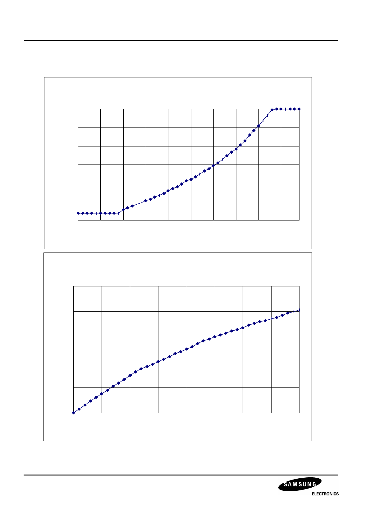
KA2506-01 I2C BUS CONTROLLED R/G/B VIDEO AMPLIFIER FOR MONITORS
Vout [dB]
Modulation Rat [%]
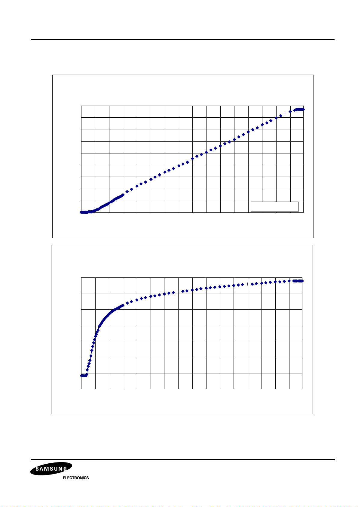
ABL Characteristic
0
-2
-4
-6
-8
-10
-12
0 0.5 1 1.5 2 2.5 3 3.5 4 4.5
BU Characteristic
25
20
15
10
5
VABL [V]
0
0 0.5 1.0 1.5 2.0 2.5 3.0 3.5 4.0
26
VBU [Vpp]
 Loading...