

Page 1
KA2142C
Vertical Deflection Output Circuit
www.fairchildsemi.com
Features
• High output current
• Pump - up circuit
• Low dissipation
• Minimum number of external parts required
• Direct drive to the deflectin coils
• Internal thermal shutdown circuit
Applications
• Power Amplifier
• Thermal Protection
• Flyback Generator
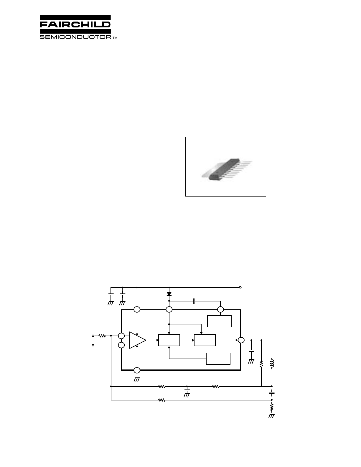
Internal Block Diagram
Description
The KA2142C is a monolithic linear IC designed for color
TV and monitor vertical deflection output. It is intended for
direct drive of the deflection coils with a high efficiency.
10-SIP H/S
+
Sawtooth IN
Vref
©2001 Fairchild Semiconductor Corporation
1
10
+
-
PRE
AMP
Vcc
(L)
Vcc
2
5
(H)
9 4
DRIVE
STAGE
+
FLYBACK
GENERATOR
OUTPUT
STAGE
THERMAL
SHUTDOWN
+
6
D.Y
+
Rev. 1.0.0
Page 2
KA2142C
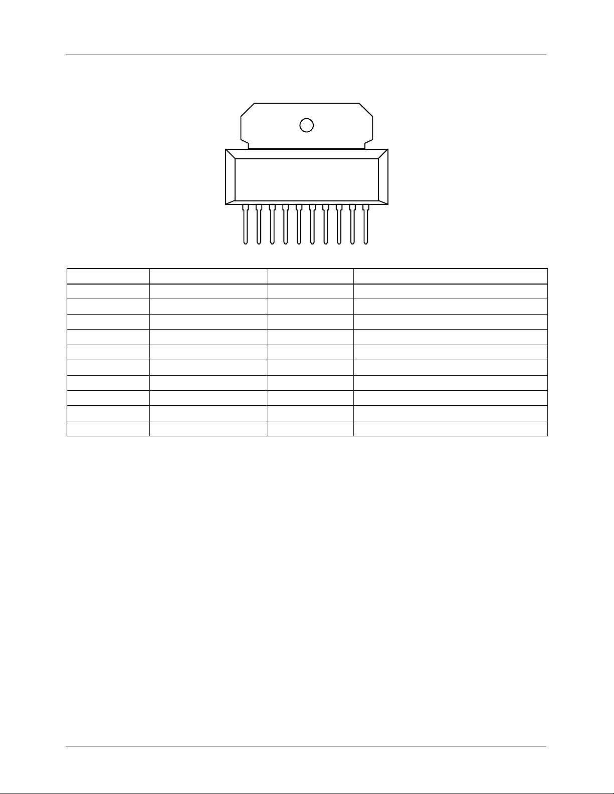
Pin Assignments
KA2142A
1 2 3 4 5 6 7
Pin Number Symbol I/O Pin Function Descrition
1 Vin ( - ) I Inverting Input
2 Vcc(L) I Supply Voltage
3- -N.C.
4 F.G O Flyback Generator
5 GND - Ground
6V
7- -N.C.
8- -N.C.
9 Vcc(H) I Output Stage Supply Voltage
10 Vin ( + ) I Non-Inverting Input
O
C
O Output
2
Page 3
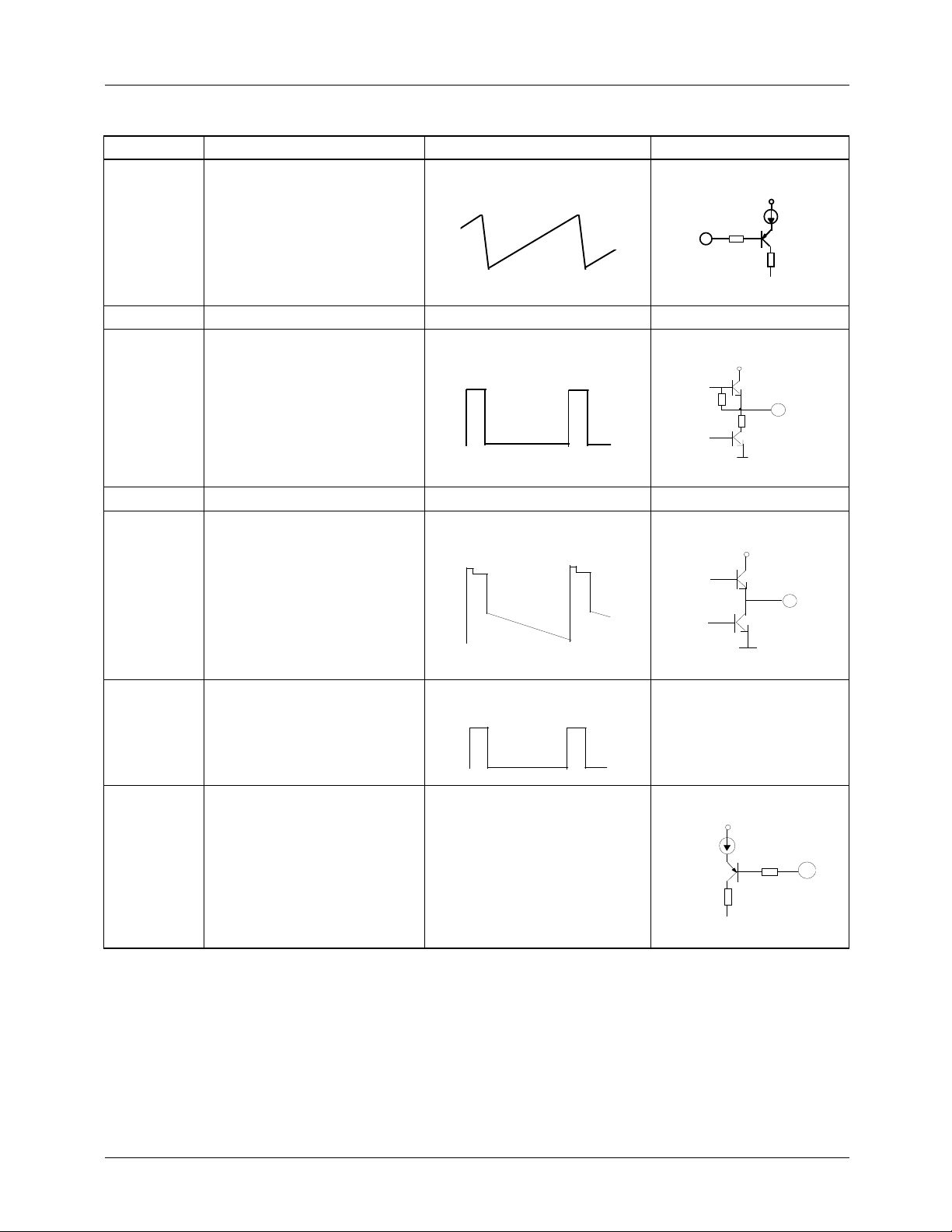
Pin Definitions
Pin Number Pin Name Waveform Equivalent Circuit
v
KA2142C
cc
1 Inverting Input
1
2 Voltage Supply DC -
4 Flyback Generator
5 Ground DC -
v
CC
6 Output Voltage
v
CC
4
6
9 Output Stage Voltage Supply -
2Vs
Vs
v
cc
10 Non-Inverting Input DC
10
3
Page 4
KA2142C
Absolute Maximum Rating ( Ta = 25oC )
Parameter Symbol Value Unit
Supply Voltage V
cc(L)
35 V
Flyback Peak Voltage V6, V9 70 V
Flyback Generator Voltage V6 35 V
Input Voltage V1, V10 V cc(L) - 0.5 V
Peak - to - Peak Output Current* Io
Peak - to - Peak Flyback Current
( f = 50 or 60Hz, Tfb ≤ 1.5mS )
Total Power Dissipation ( Ta = 25
o
C ) P
Storage Temperature Range T
Operating Ambient Temperature T
* Maximum output peak to peak current in TV or Monitor set.
I4
(p-p)
(p-p)
D
stg
opt
3A
3A
15 W
-40 ~ +150
-25 ~ +70
Thermal Data
Parameter Symbol Value Unit
Thermal Resistance Between Junction and Case R
Thermal Resistance Between Junction and Ambient R
th ( j - c )
th ( j - a)
Thermal Shut down Temperature T
tsd
12
60
150
o
o
C
C
o
C/W
o
C/W
o
C
4
Page 5

Electrical Characteristic
(Refer to the test circuit ,V cc(L)= 35V,unless otherwise specified)
Parameter Symbol Conditions Min. Typ. Max. Unit
V
Supply Voltage
Supply Quiescent Current
Pin4 Saturation Voltage to Gnd V
Saturation Voltage to supply V
Saturation Voltage to ground V
Output Center Voltage V
Input Bias Current I
CC(L)
V
CC(H)
I
CC(L)
I
CC(H)
4SAT
HSAT
LSAT
MID
BIAS
I4 = 20mA - 0.5 1 V
I6 = -1.2A - 1.6 2.2 V
I6 = -0.7A - 1.3 1.8 V
I6 = 1.2A - 1 1.4 V
I6 = 0.7A - 0.7 1 V
R1=5.6K,Rfb=45K
V1=V10=2V
V1 = 1V, V10 = 2V - -0.1 -1 µA
KA2142C
-
-
15 25 35 V
15 - 70 V
-616mA
-2236mA
-18-V
5
Page 6

KA2142C
Typical Performance Characteristic
1
0.8
0.6
V4L
0.4
0.2
0
0
Figure 1. Vs-V4L
2.5
2
1.5
V6H
1
0.5
Vs-V4L
10
Isin k-V6H
20
VS
30 40
V6L(V)
3
2
V4L
1
0
0
20
Figure 2. I4-V4L
2
1.5
1
0.5
I4-V4L
40
60 80
I4(m A)
Iso u rce -V6L
100
25
20
15
mA
10
0
0
0.4
0.8
Isink (A)
Figure 3. Isink-V6H
Vs-I2,I9
5
0
0
20
V
Figure 5. Vs-I2, I9
30
1.6
40
1.2 2
0
0
0.4
0.8
Isou rce(A)
Figure 4. Isource-V6L
1.2 2
1.6
6
Page 7

DC Test Circuit
V1
R1
Ω
12K
R2
5.6K
Ω
KA2142C
KA2142A
12345678910
C3
22p
V6
19
+
SW3
V9
R7
10K
C1
22p
Ω
V1
SW1
R6
0.1K
12
V2
+
C2
22p
SW2
R4
10KΩ
R5
Ω
0.1K
Ω
V10
R3
39K
V4
Ω
KA2142C
V10
SW4
ITEM
V1 V10 Vin1 Vin2 SW1 SW2 SW3 SW4
INPUT VOLTAGE (V) SWITCH STATE
I2, I9 - - - 2 OFF ON OFF ON
I1 1 2 - - OFF OFF OFF OFF
V4L 3 2 - - OFF OFF OFF OFF
V6L 3 2 - - OFF OFF OFF OFF
V6H 1 2 - - OFF OFF OFF OFF
7
Page 8

KA2142C
AC Test Circuit
IN4001
+
1000uF
KA2142C
KA2142A
GND
+
+
PIN9 PIN4
PIN6
3.9K
10uF
220uF
1.5Ω
220n
Ω
Output
300Ω
+
D.Y
2200uF
150n
Vref
6.8K
VS
0.1uF
PIN2
PIN10
Ω
PIN1
3.9KΩ
3.3K
Ω
Vin
1Ω
1
RA=2.7KΩ
KA551
7 8 4
6
2
+
10uF(60Hz)
5uF(12Hz
VA=7.5V
8
3
KA358
1
2
4
VCC
(7.5V)
Typical Application Circuit
Vref
0.1µF
15K
Vin
470pF
330
R2
1.2
1W
2W
Ω
Ω
Vcc=25V
+
2200µF
Ω
0.9
2W
V.D Y
6
0.22µF
22µF
+
V
OUT
3.9K
0.01
µ
0.15µF
Ω
1.5
Ω
1000µF
+
220µF
35V
4
2
IN4001
9
10
KA2142C
KA2142A
1
5
+
Ω
3.9K
Ω
6.8K
0.33µF
8
Page 9

Mechanical Dimensions
Package
#1
MAX
10-SIP H/S
1.50
0.059
()
KA2142C
Dimensions in millimeters
3.25 ±0.20
0.128 ±0.008
#10
25.75 ±0.10
1.013 ±0.004
26.05
1.026
0.50 ±0.10
0.020 ±0.004
0.50 ±0.10
1.30 ±0.10
0.051 ±0.004
2.54
0.100
1.30
0.051
()
1.65 ±0.10
0.065 ±0.004
0.020 ±0.004
7.00 ±0.30
0.276 ±0.012
1.00 ±0.20
0.039 ±0.008
8.90 ±0.20
0.350 ±0.008
13.65 ±0.30
0.537 ±0.012
16.80
0.661
MAX
23.86 ±0.20
3.80 ±0.20
0.939 ±0.008
0.150 ±0.008
9
Page 10

KA2142C
Ordering Information
Product Number Package Operating Temperature
o
KA2142C 10-SIP H/S -20
C ~ +70 oC
10
Page 11

KA2142C
11
Page 12

KA2142C
DISCLAIMER
FAIRCHILD SEMICONDUCTOR RESERVES THE RIGHT TO MAKE CHANGES WITHOUT FURT HER NOTICE TO ANY
PRODUCTS HEREI N TO IMPROVE RELIABILITY, FUNCTIO N OR DESIGN. FAIRCH IL D DOES NOT ASSUME ANY
LIABILITY ARISING OUT OF THE APPLICATION OR USE OF ANY PRODUCT OR CIRCUIT DESCRIBED HEREIN; NEITHER
DOES IT CONVEY ANY LICENSE UNDER IT S PATENT RIGHTS, NOR THE RIGHTS OF OTHE RS.
LIFE SUPPORT POL I CY
FAIRCHILD’S PR ODUCTS ARE NOT AUTH ORIZED FOR USE AS C RITICAL COMPONENT S IN LIFE SUPPORT DE VICES
OR SYSTEMS WITHOUT THE EXPRESS WRITTEN APPROVAL OF THE PRESIDENT OF FAIRCHILD SEMICONDUCTOR
CORPORATION. As used herein :
1. Life support devices or systems are devices or systems
which, (a) are intended for surgical implant into the body,
or (b) support or sustain life, and (c) whose failure to
perform when properly used in accordance with
2. A critical component in any component of a life support
device or sy stem whose fai lure to perform can be
reasonably expec ted to cause the failur e of the life support
device or system, or to affect its safety or effec t iv ene ss .
instructions for use provided in the labeling, can be
reasonably expected to result in a significant injury of the
user.
www.fairchildsemi.com
5/3/01 0.0m 001
2001 Fairchild Semiconductor Corporation
Stock#DSxxxxxxxx
 Loading...