

Page 1
K817P/ K827PH/ K847PH
Optocoupler with Phototransistor Output
Description
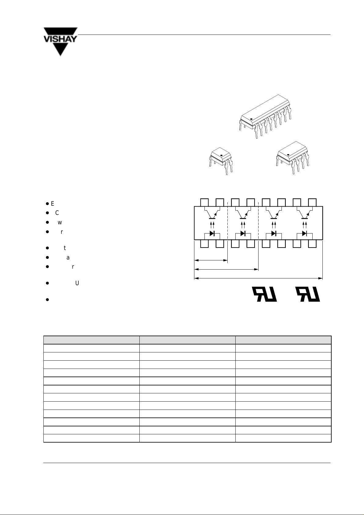
The K817P/ K827PH/ K847PH consist of a phototransistor optically coupled to a gallium arsenide
infrared-emitting diode in an 4-lead up to 16-lead
plastic dual inline package.
The elements are mounted on one leadframe using
a coplanar technique, providing a fixed distance
between input and output for highest safety
requirements.
Applications
Programmable logic controllers, modems, answering
machines, general applications
Features
D
Endstackable to 2.54 mm (0.1’) spacing
D
DC isolation test voltage V
D
Low coupling capacitance of typical 0.3 pF
D
Current Transfer Ratio (CTR) selected into
groups
D
Low temperature coefficient of CTR
D
Wide ambient temperature range
D
Underwriters Laboratory (UL) 1577 recognized,
file number E-76222
D
CSA (C–UL) 1577 recognized,
file number E-76222 – Double Protection
D
Coupling System U
= 5 kV
IO
Coll. Emitter
Anode Cath.
4 PIN
8 PIN
16 PIN
C
Vishay Telefunken
14925
13929
Order Instruction
Ordering Code CTR Ranking Remarks
K817P 50 to 600% 4 Pin = Single channel
K827PH 50 to 600% 8 Pin = Dual channel
K847PH 50 to 600% 16 Pin = Quad channel
K817P1 40 to 80% 4 Pin = Single channel
K817P2 63 to 125% 4 Pin = Single channel
K817P3 100 to 200% 4 Pin = Single channel
K817P4 160 to 320% 4 Pin = Single channel
K817P5 50 to 150% 4 Pin = Single channel
K817P6 100 to 300% 4 Pin = Single channel
K817P7 80 to 160% 4 Pin = Single channel
K827P8 130 to 260% 4 Pin = Single channel
K817P9 200 to 400% 4 Pin = Single channel
Rev. A2, 11–Jan–99 177
Page 2
K817P/ K827PH/ K847PH
Vishay Telefunken
Absolute Maximum Ratings
Input (Emitter)
Parameter Test Conditions Symbol Value Unit
Reverse voltage V
Forward current I
Forward surge current tp ≤ 10 ms I
Power dissipation T
Junction temperature T
Output (Detector)
Parameter Test Conditions Symbol Value Unit
Collector emitter voltage V
Emitter collector voltage V
Collector current I
Peak collector current tp/T = 0.5, tp ≤ 10 ms I
Power dissipation T
Junction temperature T
≤ 25°C P
amb
≤ 25°C P
amb
R
F
FSM
V
CEO
ECO
C
CM
V
6 V
60 mA
1.5 A
100 mW
j
125
°
C
70 V
7 V
50 mA
100 mA
150 mW
j
125
°
C
Coupler
Parameter Test Conditions Symbol V alue Unit
AC isolation test voltage (RMS) t = 1 min VIO
Total power dissipation T
Operating ambient temperature
range
Storage temperature range T
Soldering temperature 2 mm from case, t ≤ 10 s T
1)
Related to standard climate 23/50 DIN 50014
≤ 25°C P
amb
T
tot
amb
stg
sd
1)
5 kV
250 mW
–40 to +100
–55 to +125
260
°
C
°
C
°
C
Rev. A2, 11–Jan–99178
Page 3
K817P/ K827PH/ K847PH
C F
Vishay Telefunken
Electrical Characteristics (T
amb
= 25°C)
Input (Emitter)
Parameter Test Conditions Symbol Min. Typ. Max. Unit
Forward voltage IF = 50 mA V
Junction capacitance VR = 0 V, f = 1 MHz C
Output (Detector)
Parameter Test Conditions Symbol Min. Typ. Max. Unit
Collector emitter voltage IC = 100 mA V
Emitter collector voltage IE = 100 mA V
Collector dark current VCE = 20 V, IF = 0, E = 0 I
Coupler
Parameter Test Conditions Symbol Min. Typ. Max. Unit
Collector emitter
saturation voltage
Cut-off frequency IF = 10 mA, VCE = 5 V,
Coupling capacitance f = 1 MHz C
IF = 10 mA, IC = 1 mA V
R
L
= 100
W
F
j
CEO
ECO
CEO
CEsat
f
c
k
1.25 1.6 V
50 pF
70 V
7 V
100 nA
0.3 V
100 kHz
0.3 pF
Current Transfer Ratio (CTR)
Parameter Test Conditions Type Symbol Min. Typ. Max. Unit
IC/I
F
VCE = 5 V, IF = 5 mA K817P CTR 0.5 6.0
VCE = 5 V, IF = 5 mA K827PH CTR 0.5 6.0
VCE = 5 V, IF = 5 mA K847PH CTR 0.5 6.0
VCE = 5 V, IF = 10 mA K817P1 CTR 0.4 0.8
VCE = 5 V, IF = 10 mA K817P2 CTR 0.63 1.25
VCE = 5 V, IF = 10 mA K817P3 CTR 1.0 2.0
VCE = 5 V, IF = 10 mA K817P4 CTR 1.6 3.2
VCE = 5 V, IF = 5 mA K817P5 CTR 0.5 1.5
VCE = 5 V, IF = 5 mA K817P6 CTR 1.0 3.0
VCE = 5 V, IF = 5 mA K817P7 CTR 0.8 1.6
VCE = 5 V, IF = 5 mA K817P8 CTR 1.3 2.6
VCE = 5 V, IF = 5 mA K817P9 CTR 2.0 4.0
Rev. A2, 11–Jan–99 179
Page 4

K817P/ K827PH/ K847PH
S C L
(g)
S F L
(g)
Vishay Telefunken
Switching Characteristics
Parameter Test Conditions Symbol Typ. Unit
Delay time VS = 5 V, IC = 2 mA, RL = 100 W (see figure 1) t
Rise time
Fall time t
Storage time t
Turn-on time t
Turn-off time t
Turn-on time VS = 5 V, IF = 10 mA, RL = 1 kW (see figure 2) t
Turn-off time
d
t
r
f
s
on
off
on
t
off
3.0
3.0
4.7
0.3
6.0
5.0
9.0
18.0
m
s
m
s
m
s
m
s
m
s
m
s
m
s
m
s
+ 5 V
IC= 2 mA ;
Channel I
Channel II
W
0
RG= 50
tp
T
tp= 50 ms
95 10804
= 0.01
I
I
F
F
W
50
W
100
Figure 1. Test circuit, non-saturated operation
0
RG = 50
t
p
+
T
t
= 50 ms
p
95 10843
0.01
I
F
W
50
W
IF = 10 mA
1 k
+ 5 V
I
C
Channel I
Channel II
W
Adjusted through
input amplitude
Oscilloscope
RL= 1 M
CL= 20 pF
Oscilloscope
R
L
C
L
≥ 1 M
≤ 20 pF
W
W
I
F
0
I
C
100%
90%
10%
0
t
r
t
d
t
on
t
p
tion
t
d
t
r
t
(= td + tr) turn-on time
on
pulse duradelay time
rise time
96 11698
t
p
t
t
s
f
t
off
t
s
t
f
t
(= ts + tf) turn-off time
off
t
t
storage time
fall time
Figure 2. Test circuit, saturated operation
Figure 3. Switching times
Rev. A2, 11–Jan–99180
Page 5

K817P/ K827PH/ K847PH
Vishay Telefunken
Typical Characteristics (T
300
Coupled device
250
200
Phototransistor
150
IR-diode
100
50
tot
P – Total Power Dissipation ( mW )
0
0 40 80 120
T
96 11700
Figure 4. Total Power Dissipation vs.
1000.0
100.0
– Ambient Temperature (
amb
°
Ambient Temperature
= 25_C, unless otherwise specified)
amb
10000
VCE=20V
I
=0
1000
100
with open Base ( nA )
CEO
I – Collector Dark Current,
95 11026
F
10
1
0255075
T
– Ambient Temperature ( °C )
amb
Figure 7. Collector Dark Current vs.
Ambient Temperature
100
VCE=5V
10
100
10.0
1.0
F
I – Forward Current ( mA )
0.1
0 0.2 0.4 0.6 0.8 1.0 1.2 1.4 1.6 1.8 2.0
VF – Forward Voltage ( V )96 11862
Figure 5. Forward Current vs. Forward Voltage
2.0
VCE=5V
I
=5mA
1.5
1.0
0.5
rel
CTR – Relative Current Transfer Ratio
0
–25 0 25 50
T
– Ambient Temperature ( °C )95 11025
amb
F
75
Figure 6. Relative Current Transfer Ratio vs.
Ambient Temperature
1
0.1
C
I – Collector Current ( mA )
95 11027
0.01
0.1 1 10
IF – Forward Current ( mA )
100
Figure 8. Collector Current vs. Forward Current
100
20mA
IF=50mA
10mA
5mA
2mA
1mA
100
C
I – Collector Current ( mA )
95 10985
10
1
0.1
0.1 1 10
V
– Collector Emitter Voltage ( V )
CE
Figure 9. Collector Current vs. Collector Emitter Voltage
Rev. A2, 11–Jan–99 181
Page 6
K817P/ K827PH/ K847PH
)
Vishay Telefunken
1.0
20%
0.8
CTR=50%
0.6
0.4
0.2
0
CEsat
V – Collector Emitter Saturation Voltage ( V
110
95 11028
IC – Collector Current ( mA )
10%
100
Figure 10. Collector Emitter Saturation Voltage vs.
Collector Current
1000
VCE=5V
100
10
50
m
off
on
t / t – Turn on / Turn off Time ( s )
95 11031
Saturated Operation
V
=5V
40
30
20
10
S
R
=1k
W
L
0
0 5 10 15
– Forward Current ( mA )
I
F
t
off
t
on
20
Figure 12. Turn on / off Time vs. Forward Current
m
10
8
6
4
t
on
t
off
Non Saturated
Operation
V
=5V
S
R
=100
W
L
2
CTR – Current Transfer Ratio ( % )
95 11029
1
0.1 1 10
IF – Forward Current ( mA )
100
Figure 11. Current Transfer Ratio vs. Forward Current
Pin 1 Indication
Type
off
on
t / t – Turn on / Turn off Time ( s )
95 11030
0
02 4 6
– Collector Current ( mA )
I
C
10
Figure 13. Turn on / off Time vs. Collector Current
K817P
820UTK63
Date
Code
(YM)
Coupling
System
Indicator
Company
Logo
Figure 14. Marking example
15080
Production
Location
Rev. A2, 11–Jan–99182
Page 7
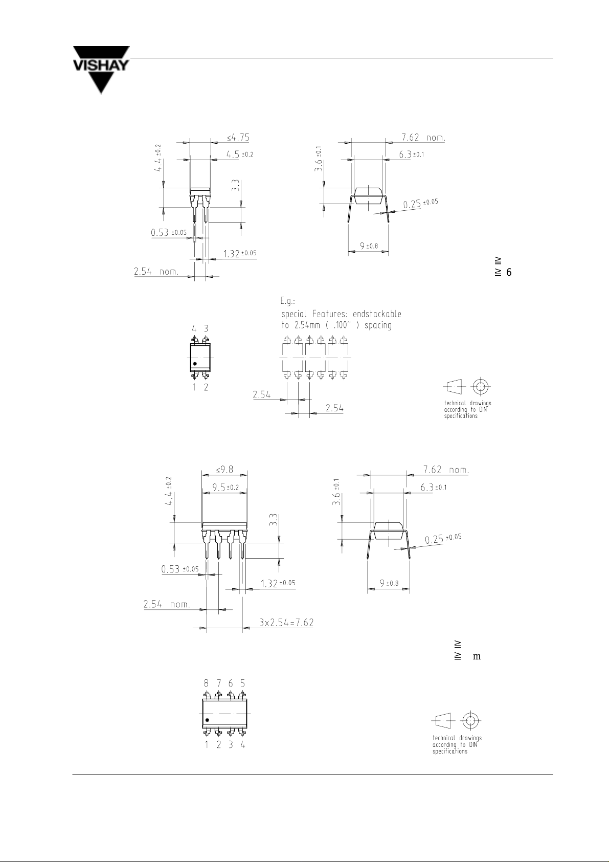
Dimensions of K817P. in mm
K817P/ K827PH/ K847PH
Vishay Telefunken
weight: ca. 0.25 g
creepage distance:y 6 mm
air path:
after mounting on PC board
y
6 mm
Dimensions of K827PH in mm
weight: ca. 0.55 g
creepage distance:
air path:
after mounting on PC board
y
y
6 mm
6 mm
14789
14784
Rev. A2, 11–Jan–99 183
Page 8

K817P/ K827PH/ K847PH
Vishay Telefunken
Dimensions of K847PH in mm
weight: ca. 1.0 g
creepage distance:y 6 mm
air path:
y
6 mm
after mounting on PC board
14783
Rev. A2, 11–Jan–99184
 Loading...