

Page 1
K6F4008U2E Family
Document Title
512K x8 bit Super Low Power and Low Voltage Full CMOS Static RAM
Revision History
CMOS SRAM
Revision No.
0.0
1.0
History
Initial Draft
Finalize
Draft Date
October 25, 2000
March 12, 2001
Remark
Preliminary
Final
The attached datasheets are provided by SAMSUNG Electronics. SAMSUNG Electronics CO., LTD. reserve the right to change the specifications and
products. SAMSUNG Electronics will answer to your questions about device. If you have any questions, please contact the SAMSUNG branch offices.
- 1 -
Revision 1.0
March 2001
Page 2
K6F4008U2E Family
CMOS SRAM
512K x 8 bit Super Low Power and Low Voltage Full CMOS Static RAM
FEATURES
• Process Technology: Full CMOS
• Organization: 512K x8 bit
• Power Supply Voltage: 2.7~3.3V
• Low Data Retention Voltage: 1.5V(Min)
• Three State Outputs
• Package Type: 48(36)-TBGA-6.00x7.00
PRODUCT FAMILY
Product Family Operating Temperature Vcc Range Speed
K6F4008U2E-F Industrial(-40~85°C) 2.7~3.3V
1. The parameter is measured with 30pF test load.
2. Typical value are at VCC=3.0V, TA=25°C and not 100% tested.
551)/70ns 1.0µA
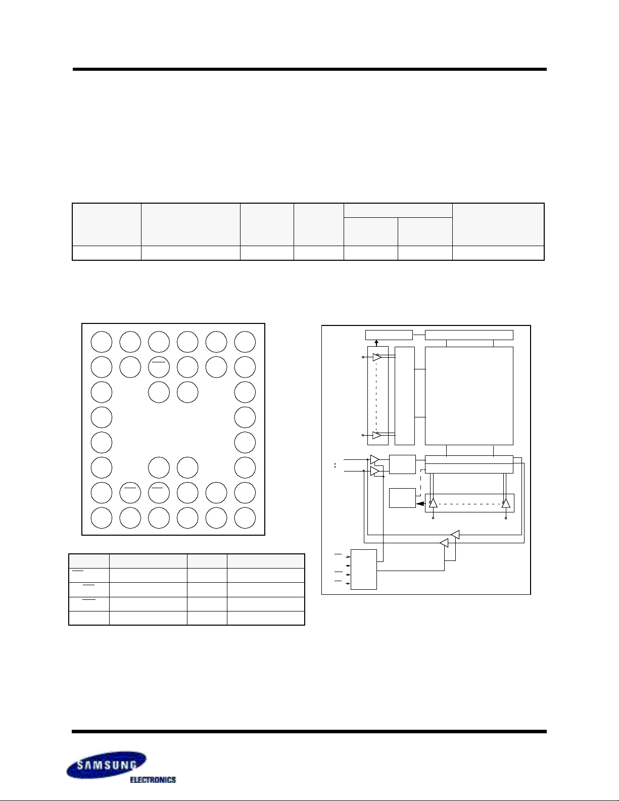
PIN DESCRIPTION
1 2 3 4 5 6
A
A0 A1 CS2 A3 A6 A8
B
I/O5 A2 WE A4 A7 I/O1
C
I/O6 DNU A5 I/O2
D
VSS VCC
48(36)-TBGA
E
VCC VSS
F
I/O7 A18 A17 I/O3
GENERAL DESCRIPTION
The K6F4008U2E families are fabricated by SAMSUNG′s
advanced full CMOS process technology. The families support
industrial temperature range and Chip Scale Package for user
flexibility of system design. The families also supports low data
retention voltage for battery back-up operation with low data
retention current.
Power Dissipation
Standby
(ISB1, Typ.)
2)
Operating
(ICC1, Max)
2mA 48(36)-TBGA-6.00x7.00
PKG Type
FUNCTIONAL BLOCK DIAGRAM
Clk gen.
Row
Address
I/O1 Data
I/O8
Row
select
cont
Precharge circuit.
Memory
Cell
Array
I/O Circuit
Column select
G
I/O8 OE CS1 A16 A15 I/O4
H
A9 A10 A11 A12 A13 A14
Name Function Name Function
CS1, CS2 Chip Select Inputs I/O1~I/O8 Data Inputs/Outputs
OE Output Enable Input Vcc Power
CS1
CS2
WE
OE
Control
logic
Data
cont
Column Address
WE Write Enable Input Vss Ground
A0~A18 Address Inputs DNU Do Not Use
SAMSUNG ELECTRONICS CO., LTD. reserves the right to change products and specifications without notice.
- 2 -
Revision 1.0
March 2001
Page 3
K6F4008U2E Family
CMOS SRAM
PRODUCT LIST
Industrial Temperature Products(-40~85°C)
Part Name Function
K6F4008U2E-EF55
K6F4008U2E-EF70
48(36)-TBGA, 55ns, 3.0V
48(36)-TBGA, 70ns, 3.0V
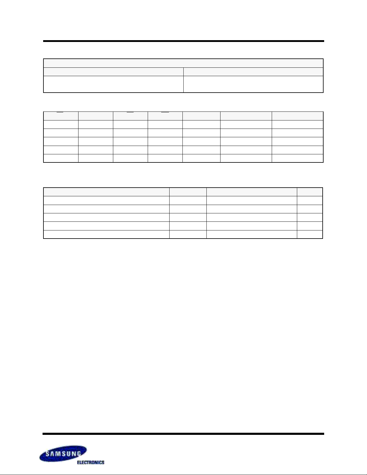
FUNCTIONAL DESCRIPTION
CS1 CS2 OE WE I/O Mode Power
H
1)
X
L H H H High-Z Output Disabled Active
L H L H Dout Read Active
L H
1. X means don′t care (Must be in low or high state)
1)
X
L
1)
X
1)
X
1)
X
1)
X
1)
X
L Din Write Active
High-Z Deselected Standby
High-Z Deselected Standby
ABSOLUTE MAXIMUM RATINGS
Item Symbol Ratings Unit
Voltage on any pin relative to Vss VIN, VOUT -0.5 to VCC+0.3V(Max. 3.6V) V
Voltage on Vcc supply relative to Vss VCC -0.3 to 3.6 V
Power Dissipation PD 1.0 W
Storage temperature TSTG -65 to 150 °C
Operating Temperature TA -40 to 85 °C
1. Stresses greater than those listed under "Absolute Maximum Ratings" may cause permanent damage to the device. Functional operation should be
restricted to recommended operating condition. Exposure to absolute maximum rating conditions for extended periods may affect reliability.
1)
- 3 -
Revision 1.0
March 2001
Page 4
K6F4008U2E Family
CMOS SRAM
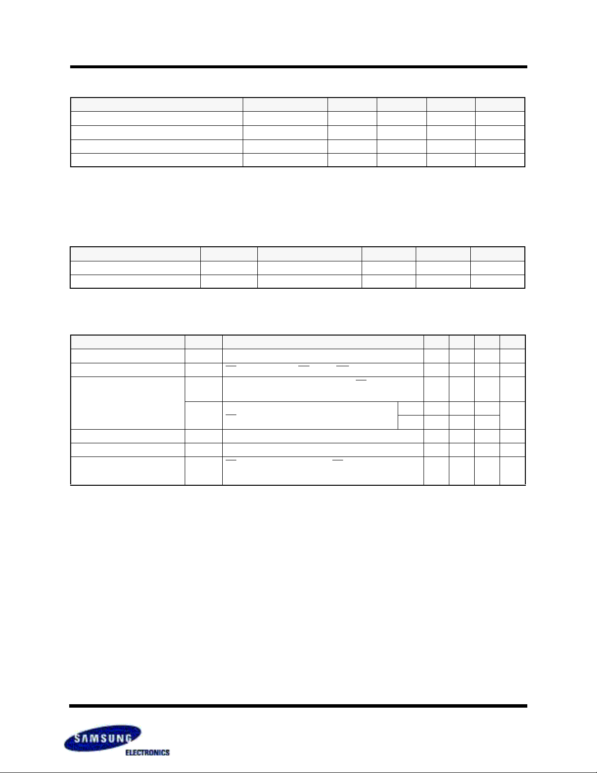
RECOMMENDED DC OPERATING CONDITIONS
Item Symbol Min Typ Max Unit
Supply voltage Vcc 2.7 3.0 3.3 V
Ground Vss 0 0 0 V
Input high voltage VIH 2.2 Input low voltage VIL
Note:
1. TA=-40 to 85°C, otherwise specified.
2. Overshoot: Vcc+2.0V in case of pulse width ≤20ns.
3. Undershoot: -2.0V in case of pulse width ≤20ns.
4. Overshoot and undershoot are sampled, not 100% tested.
CAPACITANCE
Input capacitance CIN VIN=0V - 8 pF
Input/Output capacitance CIO VIO=0V - 10 pF
1. Capacitance is sampled, not 100% tested.
1)
(f=1MHz, TA=25°C)
Item Symbol Test Condition Min Max Unit
1)
-0.3
2)
Vcc+0.3
3)
- 0.6 V
V
DC AND OPERATING CHARACTERISTICS
Item
Input leakage current ILI VIN=Vss to Vcc -1 - 1 µA
Output leakage current ILO CS1=VIH, CS2=VIL or OE=VIH or WE=VIL, VIO=Vss to Vcc -1 - 1 µA
Average operating current
Output low voltage VOL IOL = 2.1mA - - 0.4 V
Output high voltage VOH IOH = -1.0mA 2.4 - - V
Standby Current (CMOS) ISB1
Symbol
ICC1
ICC2
Test Conditions Min
Cycle time=1µs, 100%duty, IIO=0mA, CS1≤0.2V,
CS2≥Vcc-0.2V, VIN≤0.2V or VIN≥VCC-0.2V
Cycle time=Min, IIO=0mA, 100% duty,
CS1=VIL, CS2=VIH, VIN=VIL or VIH
CS1≥Vcc-0.2V, CS2≥Vcc-0.2V(CS1 controlled) or
0V≤CS2≤0.2V(CS2 controlled), Other inputs=0~Vcc
- - 2 mA
70ns - - 15
55ns - - 20
- 1 12 µA
Typ
1)
Max Unit
mA
1. Typical value are measured at VCC=3.0V, TA=25°C, and not 100% tested.
- 4 -
Revision 1.0
March 2001
Page 5
K6F4008U2E Family
AC OPERATING CONDITIONS
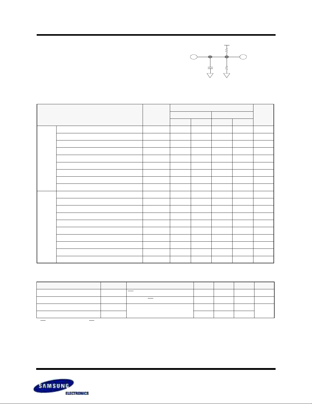
TEST CONDITIONS (Test Load and Test Input/Output Reference)
Input pulse level: 0.4 to 2.2V
Input rising and falling time: 5ns
Input and output reference voltage: 1.5V
Output load (See right): CL= 100pF+1TTL
AC CHARACTERISTICS(Vcc=2.7~3.3V, Industrial product:TA=-40 to 85°C)
Read Cycle Time tRC 55 - 70 - ns
Address Access Time tAA - 55 - 70 ns
Chip Select to Output tCO - 55 - 70 ns
Output Enable to Valid Output tOE - 25 - 35 ns
Read
Write
Chip Select to Low-Z Output tLZ 10 - 10 - ns
Output Enable to Low-Z Output tOLZ 5 - 5 - ns
Chip Disable to High-Z Output tHZ 0 20 0 25 ns
Output Disable to High-Z Output tOHZ 0 20 0 25 ns
Output Hold from Address Change tOH 10 - 10 - ns
Write Cycle Time tWC 55 - 70 - ns
Chip Select to End of Write tCW 45 - 60 - ns
Address Set-up Time tAS 0 - 0 - ns
Address Valid to End of Write tAW 45 - 60 - ns
Write Pulse Width tWP 40 - 50 - ns
Write Recovery Time tWR 0 - 0 - ns
Write to Output High-Z tWHZ 0 20 0 20 ns
Data to Write Time Overlap tDW 25 - 30 - ns
Data Hold from Write Time tDH 0 - 0 - ns
End Write to Output Low-Z tOW 5 - 5 - ns
CL=30pF+1TTL
Parameter List Symbol
Min Max Min Max
CMOS SRAM
3)
VTM
2)
R1
1)
CL
1. Including scope and jig capacitance
2. R1=3070Ω, R2=3150Ω
3. VTM =2.8V
Speed Bins
55ns 70ns
R2
2)
Units
DATA RETENTION CHARACTERISTICS
Item Symbol Test Condition Min Typ Max Unit
Vcc for data retention VDR
Data retention current IDR
Data retention set-up time tSDR
Recovery time tRDR tRC - -
1. CS1≥Vcc-0.2V, CS2≥Vcc-0.2V(CS1 controlled) or 0≤CS2≤0.2V(CS2 controlled).
2. Typical value are measured at TA=25°C and not 100% tested.
CS1≥Vcc-0.2V
Vcc=1.5V, CS1≥Vcc-0.2V1), VIN≥0V
See data retention waveform
1)
- 5 -
1.5 - 3.3 V
-
0 - -
0.5
2)
3 µA
ns
Revision 1.0
March 2001
Page 6
K6F4008U2E Family
TIMING DIAGRAMS
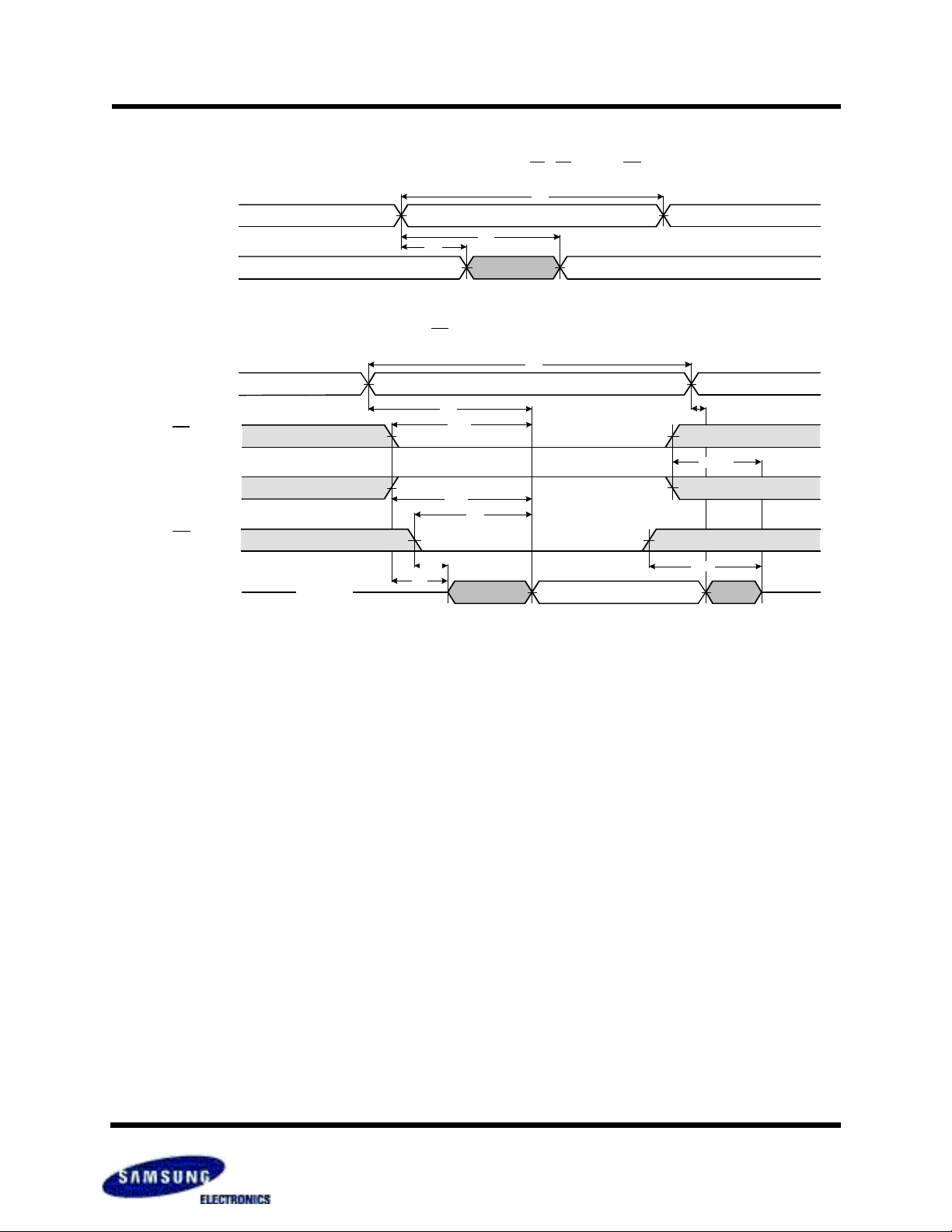
TIMING WAVEFORM OF READ CYCLE(1) (Address Controlled, CS1=OE=VIL, CS2=WE=VIH)
tRC
Address
tOH
Data Out
Previous Data Valid
TIMING WAVEFORM OF READ CYCLE(2) (WE=VIH)
Address
CS1
tAA
tRC
tAA
tCO1
CMOS SRAM
Data Valid
tOH
tHZ(1,2)
CS2
OE
Data out
NOTES (READ CYCLE)
1. tHZ and tOHZ are defined as the time at which the outputs achieve the open circuit conditions and are not referenced to output voltage
levels.
2. At any given temperature and voltage condition, tHZ(Max.) is less than tLZ(Min.) both for a given device and from device to device
interconnection.
High-Z
tLZ
tOLZ
tCO2
tOE
tOHZ
Data Valid
- 6 -
Revision 1.0
March 2001
Page 7
K6F4008U2E Family
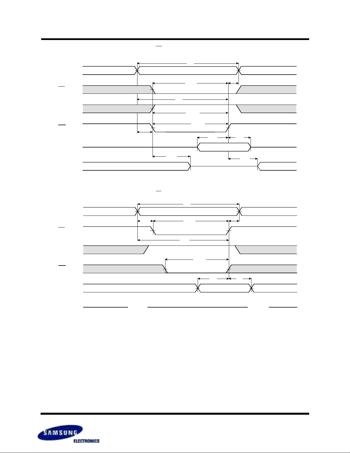
TIMING WAVEFORM OF WRITE CYCLE(1) (WE Controlled)
Address
CS1
tAW
tWC
tCW(2)
CMOS SRAM
tWR(4)
CS2
WE
tAS(3)
Data in
tWHZ
Data out
Data Undefined
TIMING WAVEFORM OF WRITE CYCLE(2) (CS1 Controlled)
Address
tAS(3)
CS1
CS2
WE
Data in
tWC
tCW(2)
tAW
tCW(2)
tWP(1)
tDW tDH
Data Valid
tOW
tWR(4)
tWP(1)
tDW tDH
Data Valid
Data out
High-Z
- 7 -
High-Z
Revision 1.0
March 2001
Page 8
K6F4008U2E Family
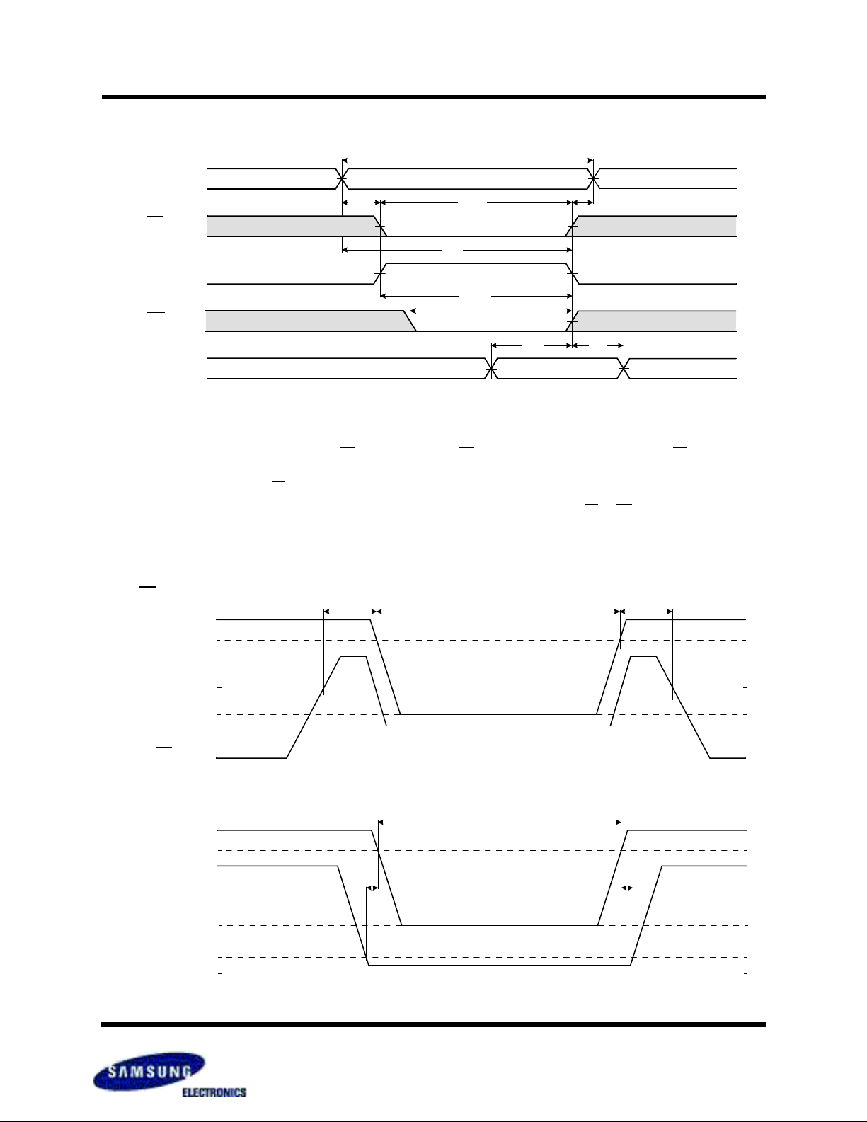
TIMING WAVEFORM OF WRITE CYCLE(3) (CS2 Controlled)
Address
CMOS SRAM
tWC
tAS(3)
CS1
CS2
WE
Data in Data Valid
Data out
NOTES (WRITE CYCLE)
1. A write occurs during the overlap of a low CS1, a high CS2 and a low WE. A write begins at the latest transition among CS1 goes low,
CS2 going high and WE going low: A write end at the earliest transition among CS1 going high, CS2 going low and WE going high, tWP
is measured from the begining of write to the end of write.
2. tCW is measured from the CS1 going low or CS2 going high to the end of write.
3. tAS is measured from the address valid to the beginning of write.
4. tWR is measured from the end of write to the address change. tWR1 applied in case a write ends as CS1 or WE going high tWR2 applied
in case a write ends as CS2 going to low.
High-Z
tAW
tCW(2)
tCW(2)
tWP(1)
tDW
tWR(4)
tDH
High-Z
DATA RETENTION WAVE FORM
CS1 controlled
VCC
2.7V
tSDR
Data Retention Mode
tRDR
2.2V
VDR
CS1
GND
CS2 controlled
VCC
2.7V
CS2
VDR
0.4V
GND
tSDR
CS1≥VCC - 0.2V
Data Retention Mode
CS2≤0.2V
- 8 -
tRDR
Revision 1.0
March 2001
Page 9
K6F4008U2E Family
CMOS SRAM
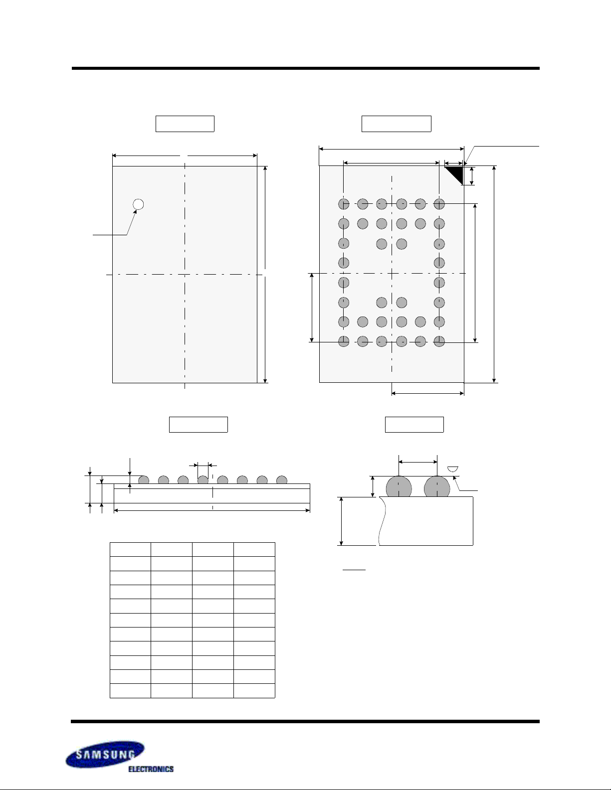
PACKAGE DIMENSIONS
48(36) TAPE BALL GRID ARRAY(0.75mm ball pitch)
B
#A1
C
Units: millimeters
Bottom ViewTop View
B
B1
6 5 4 3 2 1
A
B
C
D
E
F
C1/2
G
H
0.65
A1 INDEX MARK
0.65
C
C1
B/2
Side View
E2
E
E1
Min Typ Max
A - 0.75 B 5.90 6.00 6.10
B1 - 3.75 -
C 6.90 7.00 7.10
C1 - 5.25 -
D 0.40 0.45 0.50
E 0.80 0.90 1.00
E1 - 0.55 E2 0.30 0.35 0.40
Y - - 0.08
D
0.35/Typ.
C
0.55/Typ.
Notes.
1. Bump counts: 48(8 row x 6 column)
2. Bump pitch: (x,y)=(0.75 x 0.75)(typ.)
3. All tolerence are +/-0.050 unless
otherwise specified.
4. Typ: Typical
5. Y is coplanarity: 0.08(Max)
Detail A
A
Y
- 9 -
Revision 1.0
March 2001
Page 10

This datasheet has been downloaded from:
www.DatasheetCatalog.com
Datasheets for electronic components.
 Loading...