

Page 1

MCP MEMORYK5T6432YT(B)M
Revision 1.0
November 2001
- 1 -
Document Title
Multi-Chip Package MEMORY
64M Bit (4Mx16) Four Bank NOR Flash Memory / 32M Bit (2Mx16) UtRAM
The attached datasheets are provided by SAMSUNG Electronics. SAMSUNG Electronics CO., LTD. reserve the right to change the specifications and
products. SAMSUNG Electronics will answer to your questions about device. If you have any questions, please contact the SAMSUNG branch offices.
Revision History
Revision No.
1.0
Remark
Final
History
Final Specification
Draft Date
November 27, 2001
Page 2
MCP MEMORYK5T6432YT(B)M
Revision 1.0
November 2001
- 2 -
Multi-Chip Package MEMORY
64M Bit (4Mx16) Four Bank NOR Flash Memory / 32M Bit (2Mx16) UtRAM
The K5T6432YT(B)M featuring single 3.0V power supply is a
Multi Chip Package Memory which combines 64Mbit Four Bank
Flash and 32Mbit UtRAM.
The 64Mbit Flash memory is organized as 4M x16 bit and 32Mbit
UtRAM is organized as 2M x16 bit. The 64Mbit Flash memory is
the high performance non-volatile memory fabricated by CMOS
technology for peripheral circuit and DINOR IV(Diveded bit-line
NOR IV) architecture for the memory cell. All memory blocks are
locked and can be programmed or erased, when F-WP is low.
Using Software Lock Release function, program erase operation
can be executed.
The 32Mbit UtRAM is fabricated by SAMSUNG’s advanced
CMOS technology using one transistor memory cell.
The device also supports deep power down mode for low standby
current. The K5T6432YT(B)M is suitable for use in program and
data memory of mobile communication system to reduce mount
area. This device is available in 81-ball TBGA Type package.
FEATURES
• Power Supply voltage : 2.7 to 3.3 V
• Organization
- Flash : 4,194,304 x 16 bit
- UtRAM : 2,097,152 x 16 bit
• Access Time (@2.7V)
- Flash : 85 ns, UtRAM : 100 ns
• Power Consumption (typical value)
- Flash Read Current : 20 mA (@5MHz)
Sequential Page Read Current : 5 mA (@5MHz)
Program/Erase Current : 35 mA (Max.)
Standby mode/Deep Power mode : 0.1 µA
- UtRAM Operating Current : 18 mA
Standby Current :120 µA
Deep Power Down : 5 µA
• Secode(Security Code) Block : Extra 32KW Block (Flash)
• Block Group Protection / Unprotection (Flash)
• 128 words Page Program (Flash)
• Flash Bank Size : 4Mb / 4Mb / 28Mb / 28Mb
• Flash Endurance : 100,000 Program/Erase Cycles
• Ambient Temperature : -25°C ~ 85°C
• Endurance : 100,000 Program/Erase Cycles
• Package :81 - ball TBGA Type - 10.8 x 10.4 mm, 0.8 mm pitch
GENERAL DESCRIPTION
SAMSUNG ELECTRONICS CO., LTD. reserves the right to change products and specifications without notice.
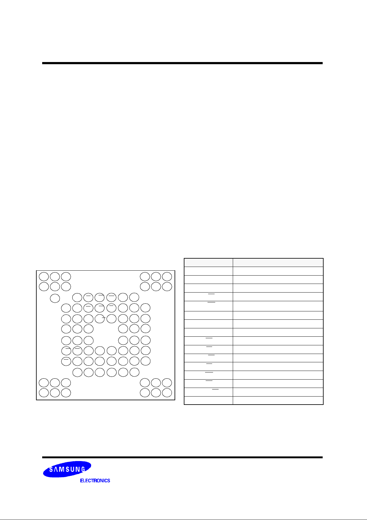
BALL CONFIGURATION BALL DESCRIPTION
Top View (Ball Down)
A
7
U
B
A
8
A3A
6
L
B
Z
Z
A19
A2A5A18
F
-RY/B
Y
A20A9
A
4
DQ6
F-CEO
E
DQ9DQ3DQ4DQ
1
3
1
2
3
4
5
6
W
E
V
S
S
A10
DQ1
A
0
A
1
A17
A11
A
12A15
A13A2
1
A14
N.C
A16
DQ1
5
F-Vcc
7
8
N
.
C
DQ8DQ2D
Q
1
1
DQ5
DQ1
4
C
S
DQ0DQ10
VccDQ
12DQ7
Vss
N.C
N.C
N.C
910
81 Ball TBGA , 0.8mm Pitch
N.C
N.C
N.CN.
C
N.C
N.CN.
C
N.C
N.CN.
C
N.C
N.CN.
C
N.C
N.CN.
C
N.C
N.CN.
C
N.C
N.CN.
C
N.C
F-W
P
F-R
P
F-Vcc
A
B
C
D
E
F
H
G
K
J
M
L
Ball Name Description
A0 to A20 Address Input Balls (Common)
A21 Address Input Ball (Flash Memory)
DQ0 to DQ15 Data Input/Output Balls (Common)
F-RP Hardware Reset (Flash Memory)
F-WP Write Protect (Flash Memory)
F-Vcc Power Supply (Flash Memory)
Vcc Power Supply (UtRAM))
Vss Ground (Common)
UB Upper Byte Enable (UtRAM)
LB Lower Byte Enable (UtRAM)
F-CE Chip Enable (Flash Memory)
ZZ Deep Power Down (UtRAM)
WE Write Enable (Common)
OE Output Enable (Common)
F-RY/BY Ready/Busy (Flash memory)
N.C No Connection
1
1
1
2
Page 3
MCP MEMORYK5T6432YT(B)M
Revision 1.0
November 2001
- 3 -
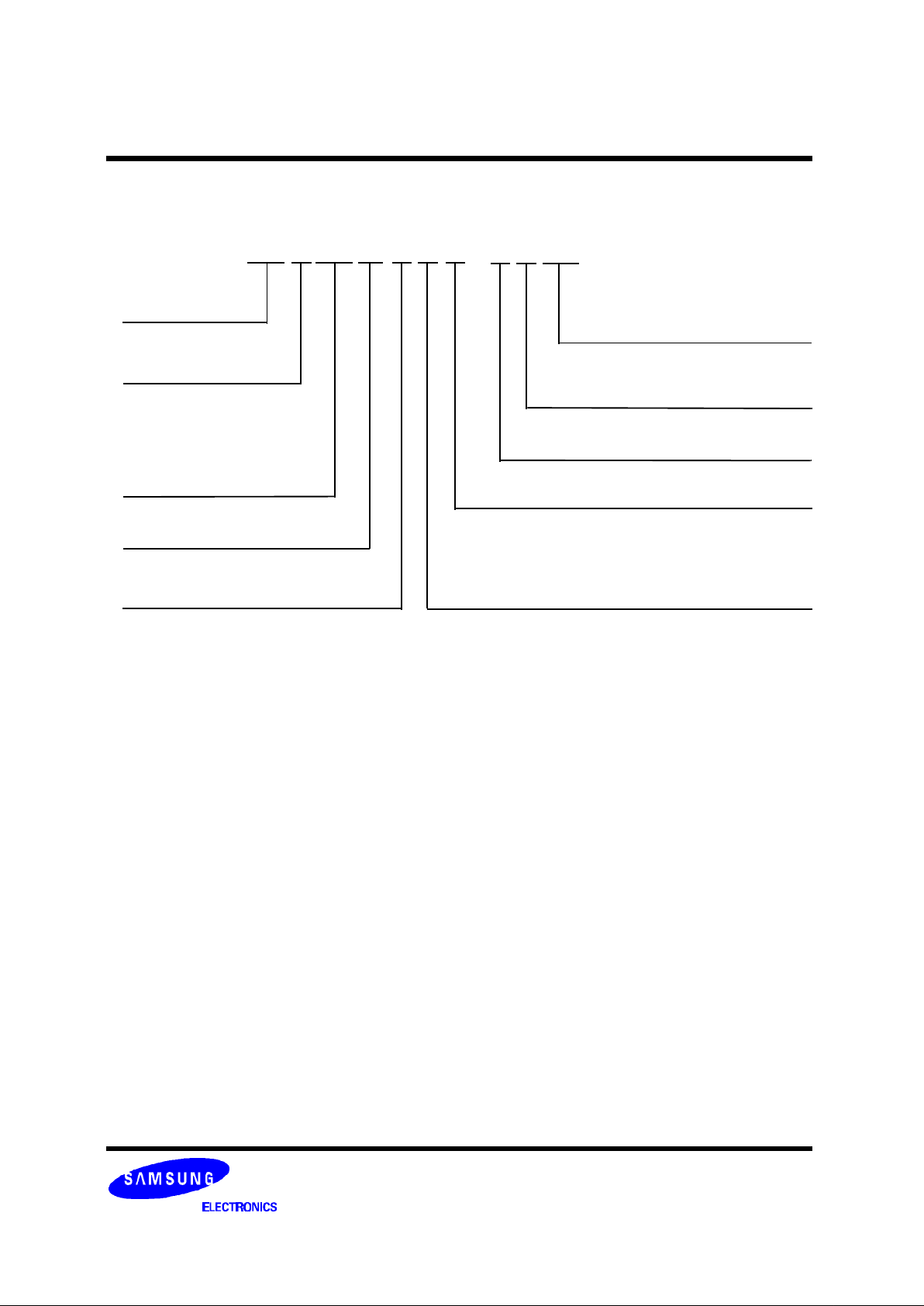
ORDERING INFORMATION
K 5 T 64 32 Y T M - T 3 10
Samsung
MCP Memory
Device Type
Mitsubishi NOR Flash
+ UtRAM
NOR Flash Density
(Organization) , (BankSize)
64 : 64Mbit (x16 Selectable)
(4Mb, 4Mb, 28Mb,2 8Mb)
Block Architecture
T = Top Boot Block
B = Bottom Boot Block
Version
M = 1st Generation
UtRAM Access Time
10 = 100 ns
Operating Voltage Range
2.7V to 3.3V
Package
T = 81 TBGA
UtRAM Density , Organization
32Mbit , x16 Selectable
Flash Access Time
3 = 85 ns
Page 4
MCP MEMORYK5T6432YT(B)M
Revision 1.0
November 2001
- 4 -
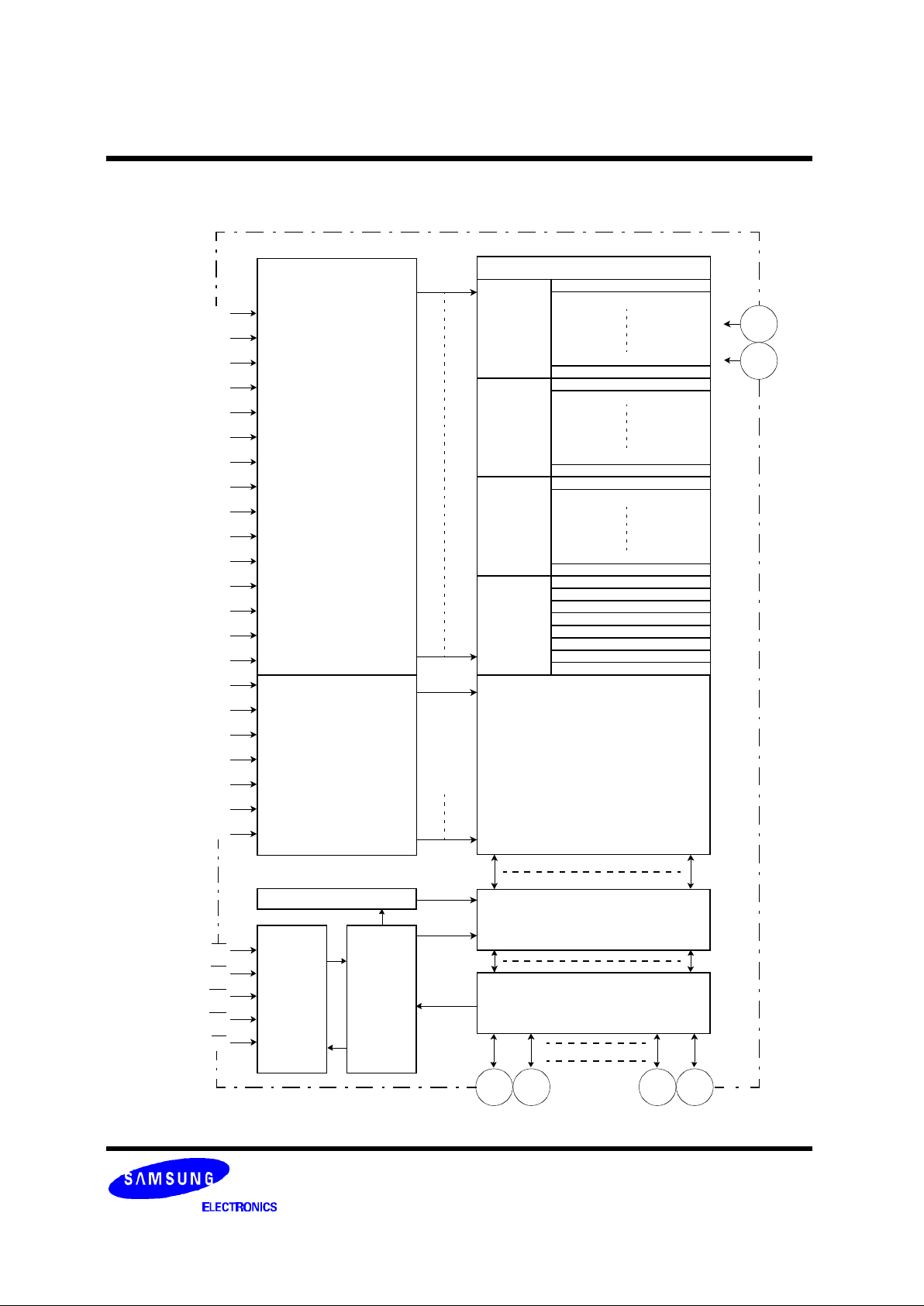
A21
A20
A19
A18
A17
A16
A15
A14
A13
A12
A11
A10
A9
A8
A7
A6
A5
A4
A3
A2
A1
A0
F-CE
OE
WE
F-WP
F-RP
Command
User
Interface
Write
State
Machine
Status/ ID Register
Y-Decorder
X-decorder
Address
Input
Chip Enable
Output Enable
Write Enable
Write Protect
Reset
/PowerDown
Main Block 14 32K-word
Main Block 8 32K-word
Parameter Block 7 4K-word
Parameter Block 2 4K-word
Boot Block 1 4K-word
Bppt Block 0 4K-word
Main Block 22 32K-word
Main Block 15 32K-word
Main Block 78 32K-word
Main Block 23 32K-word
Main Block 134 32K-word
Main Block 79 32K-word
Y-Gate / Sense Amp.
Bank4
56 blocks
Bank3
56 blocks
Bank2
8 blocks
Bank1
15 blocks
Multi Plexer
I/O Buffer
DQ15 DQ14 DQ1 DQ0
Data I/O
128-word Page Buffer
F-Vcc
Vss
FUNCTIONAL BLOCK DIAGRAM (64Mbit Flash Memory)
Flash Memory Part
Page 5

MCP MEMORYK5T6432YT(B)M
Revision 1.0
November 2001
- 5 -
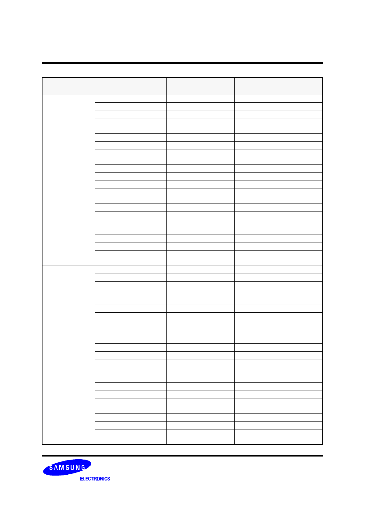
Table 1. Flash Memory Top Boot Block Address (K5T6432YT)
K5T6432YT Block Block Size
Address Range
Word Mode (x16)
Bank4
BA134 4 Kwords 3FF000H-3FFFFFH
BA133 4 Kwords 3FE000H-3FEFFFH
BA132 4 Kwords 3FD000H-3FDFFFH
BA131 4 Kwords 3FC000H-3FCFFFH
BA130 4 Kwords 3FB000H-3FBFFFH
BA129 4 Kwords 3FA000H-3FAFFFH
BA128 4 Kwords 3F9000H-3F9FFFH
BA127 4 Kwords 3F8000H-3F8FFFH
BA126 32 Kwords 3F0000H-3F7FFFH
BA125 32 Kwords 3E8000H-3EFFFFH
BA124 32 Kwords 3E0000H-3E7FFFH
BA123 32 Kwords 3D8000H-3DFFFFH
BA122 32 Kwords 3D0000H-3D7FFFH
BA121 32 Kwords 3C8000H-3CFFFFH
BA120 32 Kwords 3C0000H-3C7FFFH
Bank3
BA119 32 Kwords 3B8000H-3BFFFFH
BA118 32 Kwords 3B0000H-3B7FFFH
BA117 32 Kwords 3A8000H-3AFFFFH
BA116 32 Kwords 3A0000H-3A7FFFH
BA115 32 Kwords 398000H-39FFFFH
BA114 32 Kwords 390000H-397FFFH
BA113 32 Kwords 388000H-38FFFFH
BA112 32 Kwords 380000H-387FFFH
Bank2
BA111 32 Kwords 378000H-37FFFFH
BA110 32 Kwords 370000H-377FFFH
BA109 32 Kwords 368000H-36FFFFH
BA108 32 Kwords 360000H-367FFFH
BA107 32 Kwords 358000H-35FFFFH
BA106 32 Kwords 350000H-357FFFH
BA105 32 Kwords 348000H-34FFFFH
BA104 32 Kwords 340000H-347FFFH
BA103 32 Kwords 338000H-33FFFFH
BA102 32 Kwords 330000H-337FFFH
BA101 32 Kwords 328000H-32FFFFH
BA100 32 Kwords 320000H-327FFFH
BA99 32 Kwords 318000H-31FFFFH
BA98 32 Kwords 310000H-317FFFH
BA97 32 Kwords 208000H-20FFFFH
BA96 32 Kwords 300000H-307FFFH
BA95 32 Kwords 2F8000H-2FFFFFH
BA94 32 Kwords 2F0000H-2F7FFFH
BA93 32 Kwords 2E8000H-2EFFFFH
BA92 32 Kwords 2E0000H-2E7FFFH
BA91 32 Kwords 2D8000H-2DFFFFH
BA90 32 Kwords 2D0000H-2D7FFFH
Page 6

MCP MEMORYK5T6432YT(B)M
Revision 1.0
November 2001
- 6 -
Table 1. Flash Memory Top Boot Block Address (K5T6432YT)
K5T6432YT Block Block Size
Address Range
Word Mode (x16)
Bank2
BA89 32 Kwords 2C8000H-2CFFFFH
BA88 32 Kwords 2C0000H-2C7FFFH
BA87 32 Kwords 2B8000H-2BFFFFH
BA86 32 Kwords 2B0000H-2B7FFFH
BA85 32 Kwords 2A8000H-2AFFFFH
BA84 32 Kwords 2A0000H-2A7FFFH
BA83 32 Kwords 298000H-29FFFFH
BA82 32 Kwords 290000H-297FFFH
BA81 32 Kwords 288000H-28FFFFH
BA80 32 Kwords 280000H-287FFFH
BA79 32 Kwords 278000H-27FFFFH
BA78 32 Kwords 270000H-277FFFH
BA77 32 Kwords 268000H-26FFFFH
BA76 32 Kwords 260000H-267FFFH
BA75 32 Kwords 258000H-25FFFFH
BA74 32 Kwords 250000H-257FFFH
BA73 32 Kwords 248000H-24FFFFH
BA72 32 Kwords 240000H-247FFFH
BA71 32 Kwords 238000H-23FFFFH
BA70 32 Kwords 230000H-237FFFH
BA69 32 Kwords 228000H-22FFFFH
BA68 32 Kwords 220000H-227FFFH
BA67 32 Kwords 218000H-21FFFFH
BA66 32 Kwords 210000H-217FFFH
BA65 32 Kwords 208000H-20FFFFH
BA64 32 Kwords 200000H-207FFFH
BA63 32 Kwords 1F8000H-1FFFFFH
BA62 32 Kwords 1F0000H-1F7FFFH
BA61 32 Kwords 1E8000H-1EFFFFH
BA60 32 Kwords 1E0000H-1E7FFFH
BA59 32 Kwords 1D8000H-1DFFFFH
BA58 32 Kwords 1D0000H-1D7FFFH
BA57 32 Kwords 1C8000H-1CFFFFH
BA56 32 Kwords 1C0000H-1C7FFFH
Bank1
BA55 32 Kwords 1B8000H-1BFFFFH
BA54 32 Kwords 1B0000H-1B7FFFH
BA53 32 Kwords 1A8000H-1AFFFFH
BA52 32 Kwords 1A0000H-1A7FFFH
BA51 32 Kwords 198000H-19FFFFH
BA50 32 Kwords 190000H-197FFFH
BA49 32 Kwords 188000H-18FFFFH
BA48 32 Kwords 180000H-187FFFH
BA47 32 Kwords 178000H-17FFFFH
BA46 32 Kwords 170000H-177FFFH
BA45 32 Kwords 168000H-16FFFFH
Page 7

MCP MEMORYK5T6432YT(B)M
Revision 1.0
November 2001
- 7 -
Table 1. Flash Memory Top Boot Block Address (K5T6432YT)
K5T6432YT Block Block Size
Address Range
Word Mode (x16)
Bank1
BA44 32 Kwords 160000H-167FFFH
BA43 32 Kwords 158000H-15FFFFH
BA42 32 Kwords 150000H-157FFFH
BA41 32 Kwords 148000H-14FFFFH
BA40 32 Kwords 140000H-147FFFH
BA39 32 Kwords 138000H-13FFFFH
BA38 32 Kwords 130000H-137FFFH
BA37 32 Kwords 128000H-12FFFFH
BA36 32 Kwords 120000H-127FFFH
BA35 32 Kwords 118000H-11FFFFH
BA34 32 Kwords 110000H-117FFFH
BA33 32 Kwords 108000H-10FFFFH
BA32 32 Kwords 100000H-107FFFH
BA31 32 Kwords F8000H-FFFFFH
BA30 32 Kwords F0000H-F7FFFH
BA29 32 Kwords E8000H-EFFFFH
BA28 32 Kwords E0000H-E7FFFH
BA27 32 Kwords D8000H-DFFFFH
BA26 32 Kwords D0000H-D7FFFH
BA25 32 Kwords C8000H-CFFFFH
BA24 32 Kwords C0000H-C7FFFH
BA23 32 Kwords B8000H-BFFFFH
BA22 32 Kwords B0000H-B7FFFH
BA21 32 Kwords A8000H-AFFFFH
BA20 32 Kwords A0000H-A7FFFH
BA19 32 Kwords 98000H-9FFFFH
BA18 32 Kwords 90000H-97FFFH
BA17 32 Kwords 88000H-8FFFFH
BA16 32 Kwords 80000H-87FFFH
BA15 32 Kwords 78000H-7FFFFH
BA14 32 Kwords 70000H-77FFFH
BA13 32 Kwords 68000H-6FFFFH
BA12 32 Kwords 60000H-67FFFH
BA11 32 Kwords 58000H-5FFFFH
BA10 32 Kwords 50000H-57FFFH
BA9 32 Kwords 48000H-4FFFFH
BA8 32 Kwords 40000H-47FFFH
BA7 32 Kwords 38000H-3FFFFH
BA6 32 Kwords 30000H-37FFFH
BA5 32 Kwords 28000H-2FFFFH
BA4 32 Kwords 20000H-27FFFH
BA3 32 Kwords 18000H-1FFFFH
BA2 32 Kwords 10000H-17FFFH
BA1 32 Kwords 08000H-0FFFFH
BA0 32 Kwords 00000H-07FFFH
Page 8
MCP MEMORYK5T6432YT(B)M
Revision 1.0
November 2001
- 8 -
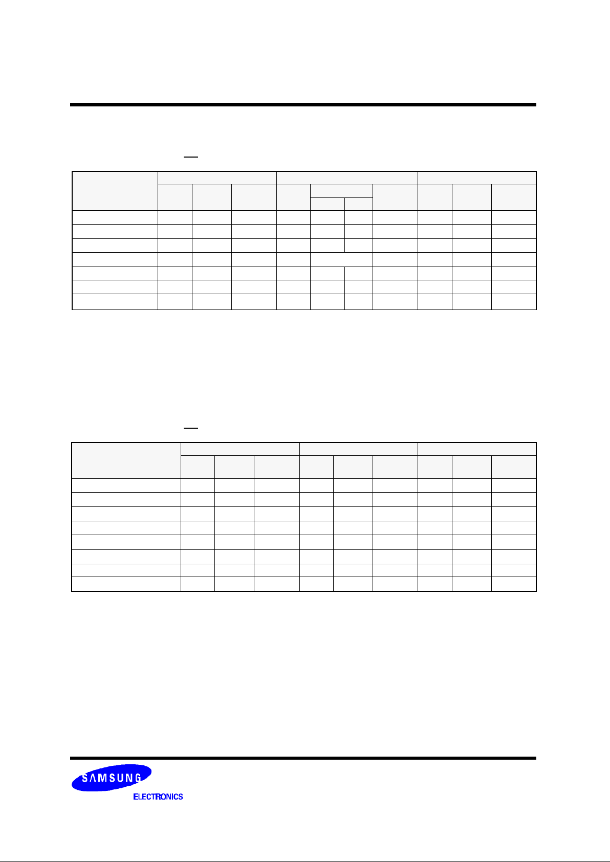
Table 2. Flash Memory Bottom Boot Block Address (K5T6432YB)
K5T6432YB Block Block Size
Address Range
Word Mode (x16)
Bank4
BA134 32 Kwords 3F8000H-3FFFFFH
BA133 32 Kwords 3F0000H-3F7FFFH
BA132 32 Kwords 3E8000H-3EFFFFH
BA131 32 Kwords 3E0000H-3E7FFFH
BA130 32 Kwords 3D8000H-3DFFFFH
BA129 32 Kwords 3D0000H-3D7FFFH
BA128 32 Kwords 3C8000H-3CFFFFH
BA127 32 Kwords 3C0000H-3C7FFFH
BA126 32 Kwords 3B8000H-3BFFFFH
BA125 32 Kwords 3B0000H-3B7FFFH
BA124 32 Kwords 3A8000H-3AFFFFH
BA123 32 Kwords 3A0000H-3A7FFFH
BA122 32 Kwords 398000H-39FFFFH
BA121 32 Kwords 390000H-397FFFH
BA120 32 Kwords 388000H-38FFFFH
BA119 32 Kwords 380000H-387FFFH
BA118 32 Kwords 378000H-37FFFFH
BA117 32 Kwords 370000H-377FFFH
BA116 32 Kwords 368000H-36FFFFH
BA115 32 Kwords 360000H-367FFFH
BA114 32 Kwords 358000H-35FFFFH
BA113 32 Kwords 350000H-357FFFH
BA112 32 Kwords 348000H-34FFFFH
BA111 32 Kwords 340000H-347FFFH
BA110 32 Kwords 338000H-33FFFFH
BA109 32 Kwords 330000H-337FFFH
BA108 32 Kwords 328000H-32FFFFH
BA107 32 Kwords 320000H-327FFFH
BA106 32 Kwords 318000H-31FFFFH
BA105 32 Kwords 310000H-317FFFH
BA104 32 Kwords 208000H-20FFFFH
BA103 32 Kwords 300000H-307FFFH
BA102 32 Kwords 2F8000H-2FFFFFH
BA101 32 Kwords 2F0000H-2F7FFFH
BA100 32 Kwords 2E8000H-2EFFFFH
BA99 32 Kwords 2E0000H-2E7FFFH
BA98 32 Kwords 2D8000H-2DFFFFH
BA97 32 Kwords 2D0000H-2D7FFFH
BA96 32 Kwords 2C8000H-2CFFFFH
BA95 32 Kwords 2C0000H-2C7FFFH
BA94 32 Kwords 2B8000H-2BFFFFH
BA93 32 Kwords 2B0000H-2B7FFFH
BA92 32 Kwords 2A8000H-2AFFFFH
BA91 32 Kwords 2A0000H-2A7FFFH
BA90 32 Kwords 298000H-29FFFFH
Page 9

MCP MEMORYK5T6432YT(B)M
Revision 1.0
November 2001
- 9 -
Table 2. Flash Memory Bottom Boot Block Address (K5T6432YB)
K5T6432YB Block Block Size
Address Range
Word Mode (x16)
Bank4
BA89 32 Kwords 290000H-297FFFH
BA88 32 Kwords 288000H-28FFFFH
BA87 32 Kwords 280000H-287FFFH
BA86 32 Kwords 278000H-27FFFFH
BA85 32 Kwords 270000H-277FFFH
BA84 32 Kwords 268000H-26FFFFH
BA83 32 Kwords 260000H-267FFFH
BA82 32 Kwords 258000H-25FFFFH
BA81 32 Kwords 250000H-257FFFH
BA80 32 Kwords 248000H-24FFFFH
BA79 32 Kwords 240000H-247FFFH
Bank3
BA78 32 Kwords 238000H-23FFFFH
BA77 32 Kwords 230000H-237FFFH
BA76 32 Kwords 228000H-22FFFFH
BA75 32 Kwords 220000H-227FFFH
BA74 32 Kwords 218000H-21FFFFH
BA73 32 Kwords 210000H-217FFFH
BA72 32 Kwords 208000H-20FFFFH
BA71 32 Kwords 200000H-207FFFH
BA70 32 Kwords 1F8000H-1FFFFFH
BA69 32 Kwords 1F0000H-1F7FFFH
BA68 32 Kwords 1E8000H-1EFFFFH
BA67 32 Kwords 1E0000H-1E7FFFH
BA66 32 Kwords 1D8000H-1DFFFFH
BA65 32 Kwords 1D0000H-1D7FFFH
BA64 32 Kwords 1C8000H-1CFFFFH
BA63 32 Kwords 1C0000H-1C7FFFH
BA62 32 Kwords 1B8000H-1BFFFFH
BA61 32 Kwords 1B0000H-1B7FFFH
BA60 32 Kwords 1A8000H-1AFFFFH
BA59 32 Kwords 1A0000H-1A7FFFH
BA58 32 Kwords 198000H-19FFFFH
BA57 32 Kwords 190000H-197FFFH
BA56 32 Kwords 188000H-18FFFFH
BA55 32 Kwords 180000H-187FFFH
BA54 32 Kwords 178000H-17FFFFH
BA53 32 Kwords 170000H-177FFFH
BA52 32 Kwords 168000H-16FFFFH
BA51 32 Kwords 160000H-167FFFH
BA50 32 Kwords 158000H-15FFFFH
BA49 32 Kwords 150000H-157FFFH
BA48 32 Kwords 148000H-14FFFFH
BA47 32 Kwords 140000H-147FFFH
BA46 32 Kwords 138000H-13FFFFH
BA45 32 Kwords 130000H-137FFFH
Page 10
MCP MEMORYK5T6432YT(B)M
Revision 1.0
November 2001
- 10 -
Table 2. Flash Memory Bottom Boot Block Address (K5T6432YB)
K5T6432YB Block Block Size
Address Range
Word Mode (x16)
Bank3
BA44 32 Kwords 128000H-12FFFFH
BA43 32 Kwords 120000H-127FFFH
BA42 32 Kwords 118000H-11FFFFH
BA41 32 Kwords 110000H-117FFFH
BA40 32 Kwords 108000H-10FFFFH
BA39 32 Kwords 100000H-107FFFH
BA38 32 Kwords F8000H-FFFFFH
BA37 32 Kwords F0000H-F7FFFH
BA36 32 Kwords E8000H-EFFFFH
BA35 32 Kwords E0000H-E7FFFH
BA34 32 Kwords D8000H-DFFFFH
BA33 32 Kwords D0000H-D7FFFH
BA32 32 Kwords C8000H-CFFFFH
BA31 32 Kwords C0000H-C7FFFH
BA30 32 Kwords B8000H-BFFFFH
BA29 32 Kwords B0000H-B7FFFH
BA28 32 Kwords A8000H-AFFFFH
BA27 32 Kwords A0000H-A7FFFH
BA26 32 Kwords 98000H-9FFFFH
BA25 32 Kwords 90000H-97FFFH
BA24 32 Kwords 88000H-8FFFFH
BA23 32 Kwords 80000H-87FFFH
Bank2
BA22 32 Kwords 78000H-7FFFFH
BA21 32 Kwords 70000H-77FFFH
BA20 32 Kwords 68000H-6FFFFH
BA19 32 Kwords 60000H-67FFFH
BA18 32 Kwords 58000H-5FFFFH
BA17 32 Kwords 50000H-57FFFH
BA16 32 Kwords 48000H-4FFFFH
BA15 32 Kwords 40000H-47FFFH
Bank1
BA14 32 Kwords 38000H-3FFFFH
BA13 32 Kwords 30000H-37FFFH
BA12 32 Kwords 28000H-2FFFFH
BA11 32 Kwords 20000H-27FFFH
BA10 32 Kwords 18000H-1FFFFH
BA9 32 Kwords 10000H-17FFFH
BA8 32 Kwords 08000H-0FFFFH
BA7 4 Kwords 07000H-07FFFH
BA6 4 Kwords 06000H-06FFFH
BA5 4 Kwords 05000H-05FFFH
BA4 4 Kwords 04000H-04FFFH
BA3 4 Kwords 03000H-03FFFH
BA2 4 Kwords 02000H-02FFFH
BA1 4 Kwords 01000H-01FFFH
BA0 4 Kwords 00000H-00FFFH
Page 11
MCP MEMORYK5T6432YT(B)M
Revision 1.0
November 2001
- 11 -
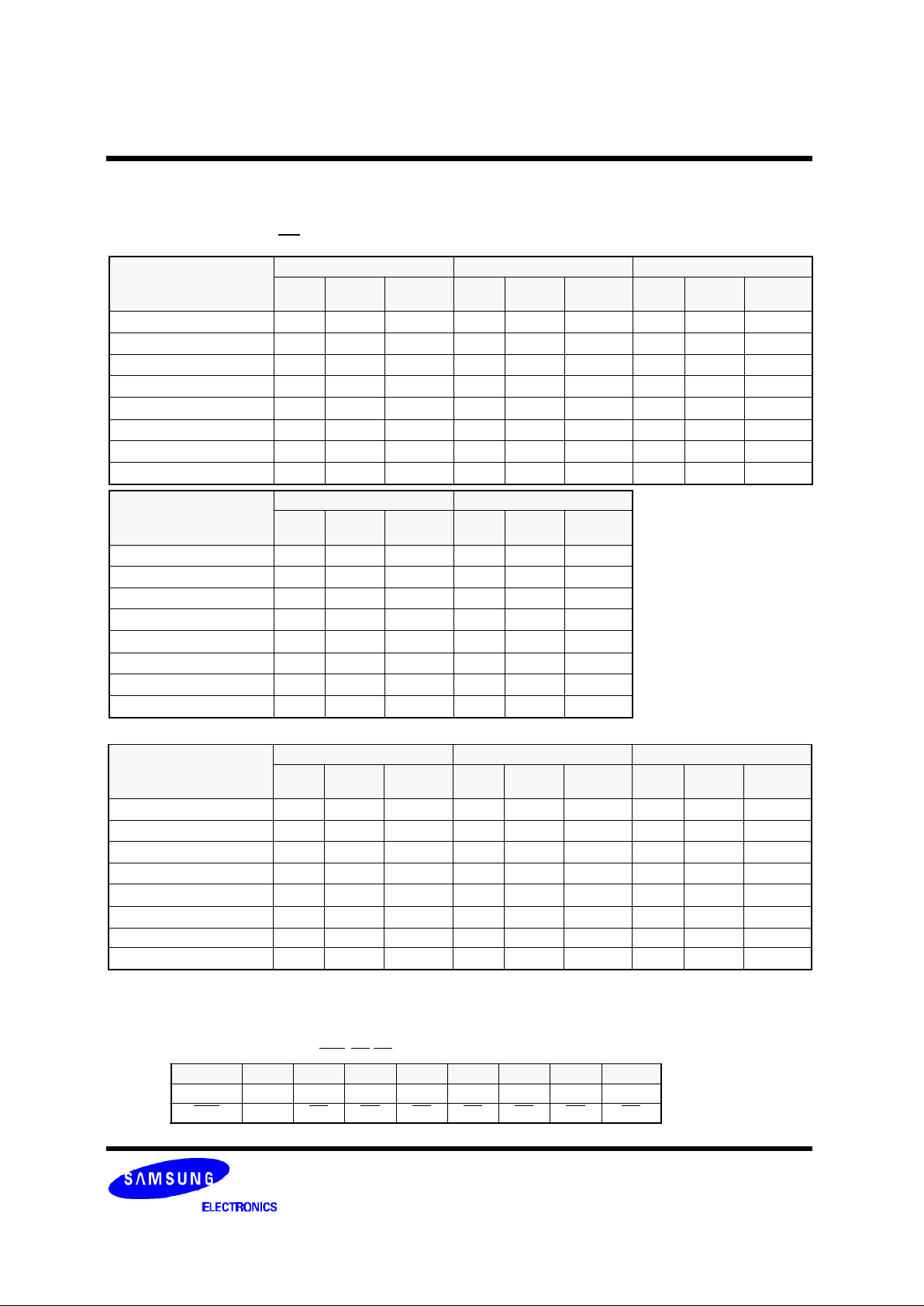
Flash MEMORY COMMAND DEFINITION
Table 3. Command List (F-WP = VIH or VIL)
Notes : 1. Upper byte data (DQ15-DQ8) is ignored.
2. Bank=Bank address (bank1-Bank4:A21-18)
3. IA=ID code address:A0=VIL (Manufacture’s code):A0=VIH (Device code), ID=ID code
4. SRD=Status Register Data
5. SA=Sequential page Address:A21-A3, A2-A0:0h
6. SA+i;A21-A3 must be flxed and A2-A0 must be incremented from 0h to 7h.
Command
1st Cycle 2nd Cycle 3rd Cycle
Mode Address
Data
1)
(DQ0-15)
Mode
Address
Data
1)
(DQ0-15)
Mode Address
Data
1)
(DQ0-15)
A21-A18 A0
Read Array Write
X
FFH
Sequential Page Read Write
X
F3H Read
SA
5)
RD0 Read
SA+i
6)
RDi
Device Identifier Write
Bank
2)
90H Read
Bank
2)
IA
3)
ID
Read Status Register Write
Bank
2)
70H Read
Bank
2)
SRD
4)
Clear Status Register Write X 50H
Suspend Write
Bank
2)
B0H
Resume Write
Bank
2)
D0H
Table 4. Command List (F-WP = VIH)
Notes : 1. Upper byte data (DQ15-DQ8) is ignored.
2. WA=Write Address, WD=Write Data
3. WA0, WAn=Write Address, WD0, WDn=Write Data, Write address and write data must be provided sequentially from 00H to 7FH
for A6-A0. Page size is 128 words (128-word x 16-bit), and also A21-A7(block address, page address) must be valid.
4. WA=Write Address:A21-A7 (block address, page address) must be valid.
5. BA=Block Address:A21-A12(Bank1), A21-A15(Bank2, Bank3, Bank4)
6. RA=Read Address:A21-A7 (block address, page address) must be valid.
Command
1st Cycle 2nd Cycle 3rd Cycle
Mode Address
Data
1)
(DQ0-15)
Mode Address
Data
1)
(DQ0-15)
Mode Address
Data
1)
(DQ0-15)
Word Program Write Bank 40H Write
WA
2)
WD
2)
Page Program Write Bank 41H Write
WA0
3)
WD0
3)
Write
WAn
3)
WDn
3)
Page Buffer to Flash Write Bank 0EH Write
WA
4)
D0
1)
Block Erase / Confirm Write Bank 20H Write
BA
5)
D0
1)
Erase All Unlocked Blocks Write X A7H Write X
D0
1)
Clear Page Buffer Write X 55H Write X
D0
1)
Single Date Load to Page Buffer Write Bank 74H Write WA WD
Flash to Page Buffer Write Bank F1H Write
RA
6)
D0
1)
Page 12
MCP MEMORYK5T6432YT(B)M
Revision 1.0
November 2001
- 12 -
Flash MEMORY COMMAND DEFINITION
Software lock release operation needs following consecutive 7bus cycles. Moreover, additional 127 bus cycles are needed for page
program operation.
Table 5. Command List (F-WP = VIH or VIL)
Setup Command for
Software Lock Release
1st Cycle 2nd Cycle 3rd Cycle
Mode Address
Data
1)
(DQ0-15)
Mode Address
Data
1)
(DQ0-15)
Mode Address
Data
1)
(DQ0-15)
Word Program Write Bank 60H Write Bank
Block
6)
Write Bank ACH
Page Program
3)
Write Bank 60H Write Bank
Block
6)
Write Bank ACH
Page Buffer to Flash Write Bank 60H Write Bank
Block
6)
Write Bank ACH
Block Erase / Confirm Write Bank 60H Write Bank
Block
6)
Write Bank ACH
Erase All Unlocked Blocks Write Bank 60H Write Bank
Block
6)
Write Bank ACH
Clear Page Buffer Write Bank 60H Write Bank
Block
6)
Write Bank ACH
Single Data Load to Page Buffer Write Bank 60H Write Bank
Block
6)
Write Bank ACH
Flash to Page Buffer Write Bank 60H Write Bank
Block
6)
Write Bank ACH
Setup Command for
Software Lock Release
4th Cycle 5th Cycle
Mode Address
Data
1)
(DQ0-15)
Mode Address
Data
1)
(DQ0-15)
Word Program Write Bank
Block
6)
Write Bank 78H
Page Program
3)
Write Bank
Block
6)
Write Bank 78H
Page Buffer to Flash Write Bank
Block
6)
Write Bank 78H
Block Erase / Confirm Write Bank
Block
6)
Write Bank 78H
Erase All Unlocked Blocks Write Bank
Block
6)
Write Bank 78H
Clear Page Buffer Write Bank
Block
6)
Write Bank 78H
Single Data Load to Page Buffer Write Bank
Block
6)
Write Bank 78H
Flash to Page Buffer Write Bank
Block
6)
Write Bank 78H
Notes : 1. Upper byte data (DQ15-DQ8) is ignored.
2. WA=Write Address, WD=Write Data
3. WA0, WAn=Write Address, WD0, WDn=Write Data, Write address and write data must be provided sequentially from 00H to 7FH
for A6-A0. Page size is 128 words (128 word x 16 bit), and also A21-A7(block address, page address) must be valid.
4. WA=Write Address:A21-A7 (block address, page address) must be valid.
5. BA=Block Address:A21-A12(Bank1), A21-A15(Bank2, Bank3, Bank4)
6. Block=Block Address:A21-A15, Block=A21-A15
Setup Command for
Software Lock Release
6th Cycle 7th Cycle 8th-134th Cycle
Mode Address
Data
1)
(DQ0-15)
Mode Address
Data
1)
(DQ0-15)
Mode Address
Data
1)
(DQ0-15)
Word Program Write Bank 40h Write
WA
2)
WD
2)
Page Program
3)
Write Bank 41h Write
WA0
3)
WD0
3)
Write
WAn
3)
WDn
3)
Page Buffer to Flash Write Bank 0Eh Write
WA
4)
D0
1)
Block Erase / Confirm Write Bank 20H Write
BA
5)
D0
1)
Erase All Unlocked Blocks Write X A7H Write X
D0
1)
Clear Page Buffer Write X 55H Write X
D0
1)
Single Data Load to Page Buffer Write Bank 74H Write WA WD
Flash to Page Buffer Write Bank F1H Write
RA
7)
D0
1)
Address DQ7 DQ6 DQ5 DQ4 DQ3 DQ2 DQ1 DQ0
Block Fixed0 A21 A20 A19 A18 A17 A16 A15
Block Fixed0 A21 A20 A19 A18 A17 A16 A15
7. RA=Read Address: A21-A7 (block address, page address) must be valid.
Page 13

MCP MEMORYK5T6432YT(B)M
Revision 1.0
November 2001
- 13 -
Table 6. Device ID Code
The output of upper byte data (DQ15-DQ7) is "0".
Code \ Pins A0 DQ7 DQ6 DQ5 DQ4 DQ3 DQ2 DQ1 DQ0 Hex Date
Manufacturer Code VIL "0" "0" "0" "1" "1" "1" "0" "0" 1CH
Devide Code (Bottom Boot) VIH "0" "0" "1" "0" "1" "0" "1" "0" 2AH
Devide Code (Top Boot) VIH "0" "0" "1" "0" "1" "0" "1" "1" 2BH
Table 7. Block Locking
F-WP pin must not be switched during performing Read / Write operations or WSM busy (WSMS=0).
F-RP F-WP
Write Protection Provided
NotesBank1 Bank2 Bank3 Bank4
Boot Parameter/Main Main Main Main
VIL x Locked Locked Locked Locked Locked Deep Power Down Mode
VIH
VIL
Locked Locked Locked
Locked
Locked
All Blocks Locked
(Valid to operate Software Lock Release)
VIH Unlocked Unlocked Unlocked Unlocked Unlocked All Blocks Unlocked
Table 8. Status Register
Symbol
(I/O Pin)
Status
Definition
"1" "0"
S.R.7 (AQ7) Write State Machine Status Ready Busy
S.R.6 (DQ6) Suspend Status Suspended Operation in Progress/Completed
S.R.5 (DQ5) Erase Status Error Successful
S.R.4 (DQ4) Program Status Error Successful
S.R.3 (DQ3) Block Status after Program Error Successful
S.R.2 (DQ2) Reserved - S.R.1 (DQ1) Reserved - S.R.0 (DQ0) Reserved - -
Table 9. Flash Memory Operation Table
Notes : 1. X cab be VIH or VIL for control pins
Mode \ Pins F-CE OE WE F-RP DQ0-15
Read
Array VIL VIL VIH VIH Data-Output
Sequential VIL VIL VIH VIH Data-Output
Status Register VIL VIL VIH VIH Status Register Data
Identifier Code VIL VIL VIH VIH Identifier Code
Output Disable VIL VIH VIH VIH High-Z
Write
Program VIL VIH VIL VIH Command / Data-In
Erase VIL VIH VIL VIH Command
Others VIL VIH VIL VIH Command
Standby VIH
X
1)
X VIH High-Z
Deep Power Down X X X VIL High-z
Page 14

MCP MEMORYK5T6432YT(B)M
Revision 1.0
November 2001
- 14 -
Flash DEVICE OPERATION
The 64Mbit DINOR IV Flash Memory includes on-chip program/erase control circuitry. The Write State Machine(WSM) control block
erase and word/page program operations. Operational modes are selected by the commands written to the Command User Interface (CUI). The Status Register indicates the status of the WSM and when the WSM successfully completes the desired program or
block erase operation.
A Deep Power Down mode is enabled when the F-RP pin is at Vss, minimizing power consumption.
Read Mode
The 64Mbit DINOR IV Flash Memory has four read modes, which accesses to the memory array, the Sequential Page Read, the
Device Identifier and the Status Register. The appropriate read commands are required to be written to the CUI. Upon initial device
power up or after exit from deep power down, the 64Mbit DINOR IV Flash Memory automatically resets to read array mode. In the
read array mode and in the conditions are low level input to OE, high level input to WE and F-RP, low level input to F-CE and
address signals to the address inputs (A21 - A0) the data of the addressed location to the data input/output (DQ15-DQ0) is output.
Standby Mode
When F-CE is at VIH, the device is in the standby mode and its power consumption is reduced. Data input/output are in a high-
impedance (High-Z) state. If the memory is deselected during block erase or program, the internal control circuits remain active and
the device consumes normal active power until the operation completes.
Output Disable
When OE is at VIH, output from the devices is disabled. Data input/output are in a high-impedance (High-Z) state.
Automatic Power Down (APD)
The Automatic Power Down minimizes the power consumption during read mode. The device automatically turns to this mode when
any addresses or F-CE isn't changed more than 200ns after the last alternation. The power consumption becomes the same as the
stand-by mode. During this mode, the output data is latched and can be read out. New data is read out correctly when addresses
are changed.
Deep Power Down
When F-RP is at VIL, the device is in the deep power down mode and its power consumption is substantially low. During read
modes, the memory is deselected and the data input/output are in a high-impedance (High-Z) state. After return from power down,
the CUI is reset to Read Array, and the Status Register is cleared to value 80H. During block erase or program modes, F-RP low will
abort either operation. Memory array data of the block being altered become invalid.
Write Mode
Writes to the CUI enables reading of memory array data, device identifiers and reading and clearing of the Status Register. They
also enable block erase and program. The CUI is written by bringing WE to low level and OE is at high level, while F-CE is at low
level. Address and data are latched on the earlier rising edge of WE and F-CE. Standard micro processor write timings are used.
Alternating Background Operation (BGO)
The 64Mbit DINOR IV Flash Memory allows to read array from one bank while the other bank operates in software command write
cycling or the erasing / programming operation in the background. Array Read operation with the other bank in BGO is performed by
changing the bank address without any additional command. When the bank address points the bank in software command write
cycling or the erasing / programming operation, the data is read out from the status register. The access time with BGO is the same
as the normal read operation. BGO must be between Bank1, Bank2, Bank3, and Bank4.
Back Bank array Read (BBR)
In the 64Mbit DINOR IV Flash Memory , when one memory address is read according to a Read Mode in the case of the same as an
access when a Read Mode command is input, an another Bank memory data can be read out (Random or Sequential Mode) by
changing an another Bank address.
Page 15

MCP MEMORYK5T6432YT(B)M
Revision 1.0
November 2001
- 15 -
Software Command Definitions
TThe device operations are selected by writing specific software command into the Commnad User Interface.
Read Array Command (FFH)
The device is in Read Array mode on initial device power up and after exit from deep power down, or by writing FFH to the Command User Interface. After starting the internal operation the device is set to the read status register mode automatically.
Sequential Page Read Command (F3H)
The Sequential Page Read command (F3H) timing can be used by writing the first command. This command is fast sequential 8
words read. During the read it is necessary to fix F-CE low and increase the addresses sequentially from 0h to 7h. The mode is kept
until Read Array command is input. The first read of Seq. Page Read timing is the same as normal read (ta(CE)). F-CE should be
fallen “L”. The read timing after the first is fast read (ta(PAD)). When an another sequential page (A21-A3) is accessed before one
sequential page (one 8-word) read is not finished, once F-CE is at VIH and A2-A0 data are 0h, after that F-CE is at VIL we can use
the first read of Seq. Page Read or normal read (ta(CE)).
Read Device Identifier Command (90H)
We can normally read device identifier codes when Read Device Identifier Code Command (90H) is written to the command latch.
Following the command write, the manufacturer code and the device code can be read from address 0000H and 0001H, respectively.
Read Status Register Command (70H)
The Status Register is read after writing the Read Status Register command of 70H to the Command User Interface. Also, after
starting the internal operation the device is set to the Read Status Register mode automatically. The contents of Status Register are
latched on the later falling edge of OE must be toggled every status read.
Clear Status Register Command (50H)
The Erase Status, Program Status and Block Status bits are set to "1"s by the Write State Machine and can only be reset by the
Clear Status Register command of 50H. These bits indicate various failure conditions. status read.
Block Erase / Confirm Command (20H/D0H)
Automated block erase is initiated by writing the Block Erase command of 20H followed by the Confirm command of D0H. An
address within the block to be erased is required. The WSM executes iterative erase pulse application and erase verify operation.
Program Commands
1) Word Program (40H)
Word program is executed by a two-command sequence. The Word program Setup command of 40H is written to the Command
Interface, followed by a second write specifying the address and data to be written. The WSM controls the program pulse application
and verify operation.
2) Page Program for Data Blocks (41H)
Page Program allows fast programming of 128words of data. Writing of 41H initiates the page program operation for the Data area.
From 2nd cycle to 129th cycle, write data must be serially inputted. Address A6-A0 have to be incremented from 00H to 7FH. After
completion of data loading, the WSM controls the program pulse application and verify operation.
3) Single Data Load to Page Buffer (74H) / Page Buffer to Flash (0EH/D0H)
Single data load to the page buffer is performed by writing 74H followed by a second write specifying the column address and data.
Distinct data up to 128word can be loaded to the page buffer by this two-command sequence. On the other hand, all of the loaded
data to the page buffer is programmed simultaneously by writing Page Buffer to Flash command of 0EH followed by the
confirm command of D0H. After completion of programming the data on the page buffer is cleared automatically.
Page 16

MCP MEMORYK5T6432YT(B)M
Revision 1.0
November 2001
- 16 -
Flash to Page Buffer Command (F1H/D0H)
Array data load to the page buffer is performed by writing the Flash to Page Buffer command of F1H followed by the Confirm command of D0H. An address within the page to be loaded is required. Then the array data can be copied into the other pages within the
same bank by using the Page Buffer to Flash command.
Clear Page Buffer Command (55H/D0H)
Loaded data to the page buffer is cleared by writing the Clear Page Buffer command of 55H followed by the Confirm command of
D0H. This command is valid for clearing data loaded by Single Data Load to Page Buffer command.
Suspend/Resume Command (B0H/D0H)
Writing the Suspend command of B0H during block erase operation interrupts the block erase operation and allows read out from
another block of memory. Writing the Suspend command of B0H during program operation interrupts the program operation and
allows read out from another block of memory. The Bank address is required when writing the Suspend/Resume Command. The
device continues to output Status Register data when read, after the Suspend command is written to it. Polling the WSM Status and
Suspend Status bits will determine when the erase operation or program operation has been suspended. At this point, writing of the
Read Array command to the CUI enables reading data from blocks other than that which is suspended. When the Resume command of D0H is written to the CUI, the WSM will continue with the erase or program processes.
Data Protection
The 64M-bit DINOR(IV) Flash Memory has a master Write Protect pin (F-WP). When F-WP is at VIH, all blocks can be programmed
or erased. When F-WP is low, all blocks are in locked mode which prevents any modifications to memory blocks. Software Lock
Release function is only command which allows to program or erase. See the BLOCK LOCKING table on 13 page for details.
Power Supply Voltage
When the power supply voltage is less than VLKO, Low Vcc Lock-Out voltage, the device is set to the Read-only mode. Regarding
DC electrical characteristics of VLKO, see 18 page. A delay time of 2us is required before any device operation is initiated. The delay
time is measured from the time Vcc reaches Vccmin (2.7V). During power up, F-RP = Vss is recommended. Falling in Busy status is
not recommended for possibility of damaging the device.
Memory Organization
The 64Mbit DINOR IV Flash Memory is constructed by 2 boot blocks of 4K words, 6 parameter blocks of 4K words and 7 main
blocks of 32K words in Bank1, by 8 main blocks of 32K words in Bank2 and by 56 main blocks of 32K words in Bank3 and Bank4.
CAPACITANCE
Item Symbol Test Condition Min Max Unit
Input Capacitance
A21-A0, OE, WE, CS2.
F-CE, F-WP, F-RP
CIN
TA=25°C,
f=1MHz,
Vin=Vout=0V
8 pF
Output Capacitance DQ15-DQ0, F-RY/BY COUT 12 pF
Page 17

MCP MEMORYK5T6432YT(B)M
Revision 1.0
November 2001
- 17 -
ABSOLUTE MAXIMUM RATINGS
Notes : 1. Minimum DC voltage is -0.5V on input / output pins. During transitions, the level may undershoot to -2.0V for periods <20ns.
Maximum DC voltage on input / output pins is F-Vcc+0.5V which, during transitions, may overshoot to F-Vcc+1.5V for periods <20ns.
Parameter Symbol Conditions Rating Unit
F-Vcc Voltage F-Vcc With Respect to Vss -0.2 to +4.6
V
All input or Output Voltage
1)
VI1 -0.6 to +4.6
Ambient Temperature Ta -40 to +85
°C
Temperature under Bias Tbs -50 to +95
Storage Temperature Tstg -65 to +125
Outputs Short Circuit Current Iout 100 (Max.) mA
Notes : All currents are in RMS unless otherwise noted
1. Typical values at F-Vcc=3.0V, Ta=25°C.
2. To protect initiation of write cycle during F-Vcc power up / down, a write cycle is locked out for F-Vcc less than VLKO, Write State Machine
is in Busy state, if F-Vcc is less than VLKO, the alteration of memory contents may occur.
Parameter
Sym-
bol
Test Conditions Min
Typ
1)
Max Unit
Input Leakage Current ILI 0V<VIN<F-Vcc
±1.0
µA
Output Leackage Current ILO 0V<VOUT<F-Vcc
±1.0
µA
Vcc Standby Current
ISB1
F-Vcc=3.3V, VIN=VIL/VIH,
F-CE=F-RP=F-WP=VIH
50 200
µA
ISB2
F-Vcc=3.3V, VIN=Vss/F-Vcc,
F-CE=F-RP=F-WP=F-Vcc±0.3V
0.1 5 µA
Vcc Deep Power Down Current
ISB3 F-Vcc=3.3V, VIN/VIH, F-RP=VIL 5 15 µA
ISB4
F-Vcc=3.3V, VIN=Vss or F-Vcc,
F-RP=F-Vss±0.3V
0.1 5 µA
Vcc Read Current for Word ICC1
F-Vcc=3.3V, VIN=VIL/VIH,
F-RP=WE=VIH,
F-CE=OE=VIL, Iout=0mA
5MHz 20 30 mA
1MHz 4 8 mA
Vcc Sequential Page Read Current ICC1P 5MHz 5 10 mA
Vcc Write Current for Word ICC2
F-Vcc=3.3V, VIN=VIL/VIH,
F-RP=OE=VIH, F-CE=WE=VIL
15 mA
Vcc Program Current ICC3
F-Vcc=3.3V, VIN=VIL/VIH,
F-CE=F-RP=F-WP=VIH
35 mA
Vcc Erase Current
ICC4
F-Vcc=3.3V, VIN=VIL/VIH,
F-CE=F-RP=F-WP=VIH
35 mA
Vcc Suspend Current
ICC5
F-Vcc=3.3V, VIN=VIL/VIH,
F-CE=F-RP=F-WP=VIH
200 mA
Input Low Voltage
VIL -0.5 0.8
V
Input High Voltage
VIH 2.0
F-Vcc
+0.5
V
Output Low Voltage VOL IOL=4.0mA 0.45 V
Output High Voltage
VOH1 IOH=-2.0mA
0.85x
F-Vcc
V
VOH2 IOL=4-100µA
F-Vcc
-0.4
V
Low F-Vcc Lock Out Voltage
2)
VLKO 1.5 2.2 V
DC CHARACTERISTICS
Page 18

MCP MEMORYK5T6432YT(B)M
Revision 1.0
November 2001
- 18 -
AC CHARACTERISTICS
Read Only Mode
Notes : 1. Timing measurements are made under AC waveforms for read operation.
Parameter Symbol
Vcc=2.7V~3.3V
Unit
Min Typ Max
Read Cycle Time tRC tAVAV 85 ns
Address Access Time ta(AD) tAVQV 85 ns
Chip Enable Access Time ta(CE) tELQV 85 ns
Output Enable Access Time ta(OE) tGLQV 30 ns
Sequential Page Access Time (After 2nd Cycle) ta(PAD) 45 ns
Sequential Page Setup Time tASPR -20 ns
Sequential Page Read F-CE "H" Time tCEHRR 15 ns
Maximum Valid Time of Sequential Page Read tRPCRR 20 ns
Chip Enable to Output in Low-Z tCLZ tELQX 0 ns
Chip Enable High to Output in High-Z tDF(CE) tEHQZ 25 ns
Output Enablr to Output in Low-Z tOLZ tGLQX 0 ns
Output Enable to High to Output in High-Z tDF(OE) tGHQZ 25 ns
F-RP Low to Output High-Z tPHZ tPLQZ 150 ns
Output Hold from F-CE , OE and Address tOH tOH 0 ns
OE hold from WE High tOEH tWHGL 10 ns
F-RP Recovery to CE Low tPS tPHEL 150 ns
Read / Write Mode (WE Control)
Notes : 1. Read timing parameters during command write operations mode are the same as during read only operation mode.
2. Typical values at F-Vcc=3.0V and Ta=25°C.
Parameter Symbol
Vcc=2.7V~3.3V
Unit
Min Typ Max
Wrie Cycle Time tWC tAVAV 85 ns
Address Setup Time tAS tAVWH 35 ns
Address Hold Time tAH tWHAX 0 ns
Data Setup time tDS tDVWH 35 ns
Data Hold time tDH tWHDX 0 ns
OE Holf from WE High tOEH tWHGL 10 ns
Chip Enable Setup Time tCS tELWL 0 ns
Chip Enable Hold Time tCH tWHEH 0 ns
Write Pulse Width tWP tWLWH 35 ns
Write Pulse Width High tWPH tWHWL 30 ns
OE Hold to WE Low tGHWL tGHWL 0 ns
Block Lock Setup to Write Enable High tBLS tPHHWH 85 ns
Block Lock Hold from Valid SRD tBLH tQVPH 0 ns
Duration of Auto Program Operation (Word Mode) tDAP tWHRH1 30
300
µs
Duration of Auto Program Operation (Page Mode) tDAP tWHRH1 4
80
ms
Duration of Auto Block Erase Operation tDAE tWHRH2 150
600
ms
Delay Time to Begin Internal Operation tWHRL tWHRL
85
ns
F-RP Recovery to F-CE Low tPS tPHWL 150 ns
Page 19

MCP MEMORYK5T6432YT(B)M
Revision 1.0
November 2001
- 19 -
AC CHARACTERISTICS
Read / Write Mode (CE Control)
Notes : 1. Timing measurements are made under AC waveforms for read operations
2. Typical values at F-Vcc=3.0V and Ta=25°C.
Parameter Symbol
Vcc=2.7V~3.3V
Unit
Min Typ Max
Write Cycle Time tWC tAVAV 85 ns
Address Setup Time tAS tAVWH 35 ns
Address Hold Time tAH tWHAX 0 ns
Data Setup Time tDS tDVWH 35 ns
Data Hold Time tDH tWHDX 0 ns
OE Hold from WE High tOEH tWHGL 10 ns
Write Enable Setup Time tWS tWLEL 0 ns
Write Enable Hold Time tWH tEHWH 0 ns
F-CE Pulse Width tCEP tELEH 35 ns
F-CE "H" Pulse Width tCEPH tEHEL 30 ns
OE Hold to WE Low tGHEL tGHEL 85 ns
Block Lock Setup to Write Enable High tBLS tPHHWH 85 ns
Block Lock Hold from Valid SRD tBLH tQVPH 0 ns
Duration of Auto Program Operation (Word Mode) tDAP tWHRH1 30 300 µs
Duration of Auto Program Operation (Page Mode) tDAP tWHRH1 4
80
ms
Duration of Auto Block Erase Operation tDAE tWHRH2 150
600
ms
Delay Time to Begin Internal Operation tEHRL tEHRL
90
ns
F-RP Recovery to F-CE Low tPS tPHWL 150 ns
Program / Erase Time
Parameter Min Typ Max Unit
Block Erase Time 150 600 ms
Main Block Write Time 1 4 sec
Page Write Time 4 80 ms
Flash to Page Buffer Time 100 150 µs
Program Suspend / Erase Suspend Time
Parameter Min Typ Max Unit
Program Suspend Time 15 µs
Erase Suspend Time 15 µs
F-Vcc Power up / Down timing
Please see 21 page.
During power up / down, by the noise pulses on control pins, the device has possibility of accidental erase of programming. The device must be
protected against initiation of write cycle for memory contents during power up / down. The delay time of min. 2 micro sec is always required
before read operation or write operation is initiated from the time F-Vcc reaches F-Vcc min. during power up /down. By holding F-RP=VIL, the
contents of memory is protected during F-Vcc power up / down. During power up, F-RP must be held VIL for min. 2us form the time F-Vcc
reaches F-Vcc min.. During power down, F-RP must be held VIL until F-Vcc reaches Vss. F-RP doesn’t have latch mode, therefore F-RP must be
held VIH during read operation or erase / program operation.
Parameter Min Typ Max Unit
tVCS F-RP=VIH Setup Time from F-Vcc min. 2 15 µs
Page 20

MCP MEMORYK5T6432YT(B)M
Revision 1.0
November 2001
- 20 -
VCC
F-RP
WE
F-CE
F-Vcc Power up / dowm Timing
tVCS
Read /Write Inhibit
VIH
VIL
3.0V
Vss
VIH
VIL
VIH
VIL
Read /Write Inhibit Read /Write Inhibit
tPS tPS
AC Waveforms for Read Operation and Test Conditions
ta(AD)
Address
tRC
ta(CE) tDF(CE)
tOEH tDF(OE)
ta(OE)
tOLZ
tCLZ
High-Z High-Z
tOH
tPHZ
tPS
Address
OE
F-CE
VIH
VIL
VIH
VIL
VIH
VIL
WE
F-RP
DATA
VIH
VIL
VIH
VIL
VIH
VIL
TEST CONDITIONS
FOR AC CHARACTERISTICS
Input Voltage: VIL=0V, VIH=Flash VCC
Input Rise and Fall Times: ≤5ns
Reference Voltage
at timing measurement: (Flash VCC)/2
Output Load: 1TTL gate + CL(30pF)
or
DUT
1.3V
1N914
3.3kohm
Page 21

MCP MEMORYK5T6432YT(B)M
Revision 1.0
November 2001
- 21 -
AC Waveforms for Sequential Page Read Operation
A21 ~ A3
F-CE
A2 ~ A0
VIH
VIL
VIH
VIL
VIH
VIL
OE
DATA
WE
VIH
VIL
VIH
VIL
VIH
VIL
ta(PAD)
Address
Address
Address 1H0H 2H 4H 5H3H 6H 7H
DOUT Valid Valid ValidValidValid Valid Valid
ta(PAD) ta(PAD) ta(PAD) ta(PAD) ta(PAD) ta(PAD)
ta(AD)
ta(CE)
F3H
High-Z
Address
Page 22

MCP MEMORYK5T6432YT(B)M
Revision 1.0
November 2001
- 22 -
AC Waveforms for Word Program Operation(WE Control)
A21 ~ A0
OE
F-CE
VIH
VIL
VIH
VIL
VIH
VIL
WE
F-RP
DATA
VIH
VIL
VIH
VIL
VIH
VIL
Bank Address
tWC
40H DIN
SR
FFH
Valid
Address Vaild Bank Address
Write Read RegisterProgram
F-WP
VIH
VIL
Address
tAS
tAH
tCS tCH ta(CE)
ta(OE)
tWP
tWPH tOEH
tDS
tWHRL
tPS
tBLS
tDAP tBLH
Busy
SR
Ready
tDH
AC Waveforms for Word Program Operation(CE Control)
A21 ~ A0
OE
F-CE
VIH
VIL
VIH
VIL
VIH
VIL
WE
F-RP
DATA
VIH
VIL
VIH
VIL
VIH
VIL
Bank Address
tWC
40H DIN
SR
FFH
Valid
Address Vaild Bank Address Valid
Write Read RegisterProgram
F-WP
VIH
VIL
Address
tAS
tAH
ta(CE)
ta(OE)
tCEP
tWH
tOEH
tDS
tEHRL
tPS
tBLS
tDAP tBLH
Busy
SR
Ready
tDH
tWS
Read Status Register
Read Status Register
High-Z
High-Z
Page 23

MCP MEMORYK5T6432YT(B)M
Revision 1.0
November 2001
- 23 -
AC Waveforms for Page Program Operation(WE Control)
A21 ~ A7
OE
F-CE
VIH
VIL
VIH
VIL
VIH
VIL
WE
F-RP
DATA
VIH
VIL
VIH
VIL
VIH
VIL
F-WP
VIH
VIL
Address
tWC
Write Read RegisterRead Status Register
00H 7FH
DIN DOU DIN DIN
SR
Busy
SR
Ready
FFH
The Other Bank
Vaild
Address Vaild
Address Vaild
Bank Address
Address Vaild Bank Address Vaild
Vaild 01H-7EH
tAS
tAH
ta(OE)
tCS tCH
ta(CE)
ta(CE)
tWP tWPH tOEH
ta(OE)
tGHWL
tOEH
tDH
High-Z
tDS
41H
tDAP
tWHRL
tBLH
tBLS
VIH
VIL
A6 ~ A0
AC Waveforms for Page Program Operation(CE Control)
A21 ~ A7
OE
F-CE
VIH
VIL
VIH
VIL
VIH
VIL
WE
F-RP
DATA
VIH
VIL
VIH
VIL
VIH
VIL
F-WP
VIH
VIL
Address
tWC
Write Read RegisterRead Status Register
00H 7FH
DIN
DOU
DIN DIN
SR
Busy
SR
Ready
FFH
The Other Bank
Vaild
Address Vaild
Address Vaild
Bank Address
Address Vaild Bank Address Vaild
Vaild 01H-7EH
tAS
tAH
ta(OE)
tWS tWH
ta(CE)
ta(CE)
tCEP
tCEPH
tOEH
ta(OE)
tGHWL
tOEH
tDH
High-Z
tDS
41H
tDAP
tEHRL
tBLH
tBLS
VIH
VIL
A6 ~ A0
tPS
Page 24

MCP MEMORYK5T6432YT(B)M
Revision 1.0
November 2001
- 24 -
AC Waveforms for Erase Operation(WE Control)
A21 ~ A0
OE
F-CE
VIH
VIL
VIH
VIL
WE
F-RP
DATA
VIH
VIL
VIH
VIL
VIH
VIL
F-WP
VIH
VIL
Address
Write Read RegisterRead Status Register
Bank Address
tBLH
tWC
VIH
VIL
Vaild
Bank Address
Address Vaild
20H DOH FFH
Erase
tAS
tAH
tCS tCH
ta(CE)
tWP
tWPH
tOEH
ta(OE)
tDS
tWHRL
tPS
tDH
tBLS
tDAE
SR
Busy
SR
Ready
AC Waveforms for Erase Operation(CE Control)
A21 ~ A0
OE
F-CE
VIH
VIL
VIH
VIL
WE
F-RP
DATA
VIH
VIL
VIH
VIL
VIH
VIL
F-WP
VIH
VIL
Address
Write Read RegisterRead Status Register
Bank Address
tBLH
tWC
VIH
VIL
Vaild
Bank Address
Address Vaild
20H DOH FFH
Erase
tAS
tAH
tWS tWH
ta(CE)
tCEP
tOEH
ta(OE)
tDS
tWHRL
tPS
tDH
tBLS
tDAE
SR
Busy
SR
Ready
High-Z
High-Z
Page 25

MCP MEMORYK5T6432YT(B)M
Revision 1.0
November 2001
- 25 -
AC Waveforms for Word Program Operation with BGO(WE Control)
A21 ~ A7
OE
F-CE
VIH
VIL
VIH
VIL
VIH
VIL
WE
DATA
VIH
VIL
VIH
VIL
VIH
VIL
Address
Read Array in another bank
Vaild
Bank Address
Address Vaild
A6 ~ A0
tWC tAS
tAH
ta(CE)
Address Vaild Address Vaild
Address Vaild Address Vaild
DIN
High-Z
40H
Change Bank Address
Read Status RegisterProgram in one bank
Address Vaild
SR
Busy
DOUT DOUT
tCS tCH
tWP
tWPH tOEH
ta(OE)
tDS
tWHRL
tDH
AC Waveforms for Word Program Operation with BGO(CE Control)
A21 ~ A7
OE
F-CE
VIH
VIL
VIH
VIL
VIH
VIL
WE
DATA
VIH
VIL
VIH
VIL
VIH
VIL
Address
Read Array in another bank
Vaild
Bank Address
Address Vaild
A6 ~ A0
tWC tAS
tAH
ta(CE)
Address Vaild Address Vaild
Address Vaild Address Vaild
DIN
High-Z
40H
Change Bank Address
Read Status RegisterProgram in one bank
Address Vaild
SR
Busy
DOUT DOUT
tWS
tCEP
tOEH
ta(OE)
tDS
tEHRL
tDH
tWH
Program
Program
Page 26

MCP MEMORYK5T6432YT(B)M
Revision 1.0
November 2001
- 26 -
AC Waveforms for Page Program Operatio with BGO(WE Control)
A21 ~ A7
OE
F-CE
VIH
VIL
VIH
VIL
VIH
VIL
WE
DATA
VIH
VIL
VIH
VIL
VIH
VIL
Address
Read Array in another bank
Vaild
Bank Address
Address Vaild
A6 ~ A0
tWC tAS
tAH
Address Vaild Address Vaild
Address Vaild Address Vaild
Change Bank Address
Program in one bank
00H 01H-7EH
DIN
High-Z
41H DOUT
tDS
DIN DIN DOUT
Valid 7FH
ta(CE)
ta(OE)ta(CE)
tCS
tCH
tWP tWPH tOEH
ta(OE)
tGHWL
tOEH
tWHRL
tDH
DOU
SR
Busy
AC Waveforms for Page Program Operatio with BGO(CE Control)
A21 ~ A7
OE
F-CE
VIH
VIL
VIH
VIL
VIH
VIL
WE
DATA
VIH
VIL
VIH
VIL
VIH
VIL
Address
Read Array in another bank
Vaild
Bank Address
Address Vaild
A6 ~ A0
tWC tAS
tAH
Address Vaild Address Vaild
Change Bank Address
Program in one bank
00H 01H-7EH
DIN
High-Z
DOUT
tDS
DIN DIN DOUT
Valid 7FH
ta(CE)
ta(OE)ta(CE)
tWS tWH
tCEP
ta(OE)
tGHEL
tOEH
tEHRL
tDH
DOUT
SR
Busy
tCEPH
tEHRL
41H
Page 27

MCP MEMORYK5T6432YT(B)M
Revision 1.0
November 2001
- 27 -
AC Waveforms for Erase Operation with BGO(WE Control)
A21 ~ A0
OE
F-CE
VIH
VIL
VIH
VIL
WE
DATA
VIH
VIL
VIH
VIL
VIH
VIL
Address
Address Vaild
tWC
Vaild
Bank Address
20H DOH
tAS
tCS tCH
ta(CE)
tWP
tWPH
tOEH
ta(OE)
tDS
tWHRL
tDH
SR
Busy
High-Z
Address Vaild
Address Vaild
tAH
DOUT DOUT
Read Array in another bank
Change Bank Address
Read Status RegisterProgram in one bank
A21 ~ A0
OE
F-CE
VIH
VIL
VIH
VIL
WE
DATA
VIH
VIL
VIH
VIL
VIH
VIL
Address
tWC
Vaild
Bank Address
20H DOH
tAS
tWS tWH
ta(CE)
tCEP
tOEH
ta(OE)
tDS
tEHRL
tDH
SR
Busy
High-Z
AC Waveforms for Erase Operation with BGO(CE Control)
Address Vaild Address Vaild
Address Vaild
Read Array in another bank
Change Bank Address
Read Status RegisterProgram in one bank
tAH
DOUT DOUT
Page 28

MCP MEMORYK5T6432YT(B)M
Revision 1.0
November 2001
- 28 -
AC Waveforms for Suspend Operation(WE Control)
Bank Address Vaild
tBLS
tCS tCH
ta(CE)
tWP
tOEH
S.R.6,7=1
SR
Busy
High-Z
tAH
Read Status Register
tAS
B0H
ta(OE)
Suspend Time
tBLH
Bank Address Vaild
A21 ~ A0
OE
F-CE
VIH
VIL
VIH
VIL
WE
F-RP
DATA
VIH
VIL
VIH
VIL
VIH
VIL
F-WP
VIH
VIL
Address
VIH
VIL
AC Waveforms for Suspend Operation(CE Control)
Bank Address Vaild
tBLS
tWS
ta(CE)
tCEP
S.R.6,7=1
SR
Busy
High-Z
tAH
Read Status Register
tAS
B0H
ta(OE)
Suspend Time
tBLH
Bank Address Vaild
A21 ~ A0
OE
F-CE
VIH
VIL
VIH
VIL
WE
F-RP
DATA
VIH
VIL
VIH
VIL
VIH
VIL
F-WP
VIH
VIL
Address
VIH
VIL
tOEH
tWH
Page 29

MCP MEMORYK5T6432YT(B)M
Revision 1.0
November 2001
- 29 -
SR.7=1?
START
Write 40H
Word Program Flow Chart
Write Address,
Data
Status Register
Read
Full Status Check
If Desired
Word Program
Completed
Suspend Loop
Write D0H
Yes
No No
Yes
n=7FH?
START
Write 41H
Page Program Flow Chart
Status Register
Read
Page Program
Completed
Suspend Loop
Write D0H
Write
Yes
No No
Yes
n = 0
Write Address n,
DATA n
SR.7=1?
Full Status Check
If Desired
BOH?
Yes
n = 0
No
Yes
SR.7=1?
START
Write 20H
Block Erase Flow Chart
Write D0H
Block Address
Status Register
Read
Full Status Check
If Desired
Erase
Completed
Suspend Loop
Write D0H
Write
Yes
No No
Yes
BOH?
SR.4,5=1?
START
Status Register Check Flow Chart
Pass
(Block Erase, Program)
YES
Command
Sequence Error
SR.5=0?
No
Block Erase
Error
No
SR.4=0?
No
Program Error
(Page Program)
YES
SR.3=0?
No
Block Erase Error
(Block Fail)
YES
YES
Yes
Yes
Write
BOH?
Page 30

MCP MEMORYK5T6432YT(B)M
Revision 1.0
November 2001
- 30 -
Load
START
Write 74H
Single Data Load to Page Buffer
Write Address,
Data
Single Data Load
To Page Buffer
No
S.R.6=1?
START
Write B0H
Suspend / Resume Flow Chart
Write FFH
Operation
Restart
Status Register
Read
Read
Write D0H
Yes
Yes
SR.7=1?
START
Write 0H
Page Buffer to Flash Flow Chart
Write D0H
Page Address
Status Register
Read
Full Status Check
If Desired
Suspend Loop
Write D0H
Write
Yes
No No
Yes
BOH?
S.R.7=1?
No
Erase/Program
Finished
Flow Chart
Completed
Finished?
Yes
Page Buffer
To Flash
Completed
Read Array
Data
Yes
Finished?
No
Suspend
Resume
START
Write 55H
Clear Page Buffer Flow Chart
Clear Page Buffer
Completed
Write D0H
No
Page 31

MCP MEMORYK5T6432YT(B)M
Revision 1.0
November 2001
- 31 -
Operation Status (WP=VIH)
Single Data Load
to Page Bufer Setup
Clear Page Bufer
Setup
Flash Page Burrer
Setup
Page Buffer to Flash
Setup
Page Program
Setup
Word Program
Setup
Block Erase
Setup
Erase All Unlocked
Blocks Setup
Read
Status Register
Program &
Read
Device Identifier
Read/Standby State
(Read Array Mode)
Read/Standby State
(Sequential Page Read Mode)
FFH (Read Array)
F3H (Seq. Page)
70H
70H
90H
90H
FFH (Read Array)
F3H (Seq. Page)
Clear
Status Register
50H
Seq. Page Read
Read Array
(From the other Bank)
Change Bank
Address
D0H WD D0H
55H F1H74H 0EH 41H 40H 20H A7H
Setup State
Verift
Read
Status Register
Erase &
Verift
Read
Status Register
Read
Status Register
Read Array
Seq. Page Read
Read Array
(From the other Bank)
Change Bank
Address
Change Bank
Address
B0H B0H
D0H D0H
D0H WD D0H D0H Other
Wdi
I=0-127Other
FFH (Read Array)
F3H (Seq. Page)
70H
Read State
with BGO
Internal State
FFH
F3H
Suspend
State
Read Array
Ready
Page 32

MCP MEMORYK5T6432YT(B)M
Revision 1.0
November 2001
- 32 -
Operation Status (WP=VIL)
Single Data Load
to Page Bufer Setup
Clear Page Bufer
Setup
Flash Page Burrer
Setup
Page Buffer to Flash
Setup
Page Program
Setup
Word Program
Setup
Block Erase
Setup
Erase All Unlocked
Blocks Setup
Program &
D0H WD D0H
55H F1H74H 0EH 41H 40H 20H A7H
Setup State
Verift
Read
Status Register
Erase &
Verift
Read
Status Register
Read
Status Register
Read Array
Seq. Page Read
Read Array
(From the other Bank)
Change Bank
Address
Change Bank
Address
B0H B0H
D0H D0H
D0H WD D0H D0H
Wdi
i=0-127
Ready
FFH (Read Array)
F3H (Seq. Page)
70H
Read State
with BGO
Internal State
Suspend
State
Read
Status Register
Read
Device Identifier
Read/Standby State
(Read Array Mode)
Read/Standby State
(Sequential Page Read Mode)
FFH (Read Array)
F3H (Seq. Page)
70H
70H
90H
90H
FFH (Read Array)
F3H (Seq. Page)
FFH
F3H
Read Array
Clear
Status Register
50H
Seq. Page Read
Read Array
(From the other Bank)
Change Bank
Address
Single Data Load
to Page Bufer Setup
BA
Single Data Load
to Page Bufer Setup
ACH
Single Data Load
to Page Bufer Setup
BA
Single Data Load
to Page Bufer Setup
60H
*
*
Single Data Load
to Page Bufer Setup
7BH
Other
Page 33

MCP MEMORYK5T6432YT(B)M
Revision 1.0
November 2001
- 33 -
FUNCTIONAL BLOCK DIAGRAM (32Mbit UtRAM)
UtRAM Part
Clk gen.
Row
select
I/O1~I/O8
Data
cont
Data
cont
Data
cont
I/O9~I/O16
Vcc
Vss
Precharge circuit.
Memory array
I/O Circuit
Column select
WE
OE
UB
CS
LB
Control Logic
ZZ
Row
Addresses
Column Addresses
FUNCTIONAL DESCRIPTION
1. X means don’t care.(Must be low or high state)
CS ZZ OE WE LB UB I/O1~8 I/O9~16 Mode Power
H H
X
1)
X
1)
X
1)
X
1)
High-Z High-Z Deselected Standby
X
1)
L
X
1)
X
1)
X
1)
X
1)
High-Z High-Z Deselected Deep Power Down
L H
X
1)
X
1)
H H High-Z High-Z Deselected Standby
L H H H L
X
1)
High-Z High-Z Output Disabled Active
L H H H
X
1)
L High-Z High-Z Output Disabled Active
L H L H L H Dout High-Z Lower Byte Read Active
L H L H H L High-Z Dout Upper Byte Read Active
L H L H L L Dout Dout Word Read Active
L H
X
1)
L L H Din High-Z Lower Byte Write Active
L H
X
1)
L H L High-Z Din Upper Byte Write Active
L H
X
1)
L L L Din Din Word Write Active
Page 34

MCP MEMORYK5T6432YT(B)M
Revision 1.0
November 2001
- 34 -
ABSOLUTE MAXIMUM RATINGS
1)
1. Stresses greater than those listed under "Absolute Maximum Ratings" may cause permanent damage to the device. Functional operation should be
restricted to recommended operating condition. Exposure to absolute maximum rating conditions longer than 1seconds may affect reliability.
Item Symbol Ratings Unit
Voltage on any pin relative to Vss VIN, VOUT -0.2 to VCC+0.3V V
Voltage on Vcc supply relative to Vss VCC -0.2 to 3.6V V
Power Dissipation PD 1.0 W
Storage temperature TSTG -65 to 150 °C
Operating Temperature TA -25 to 85 °C
ZZ=VIL
CS=VIH
ZZ=VIL
CS=VIL, UB or/and LB=VIL
ZZ=VIH
CS=VIH, ZZ=VIH
STANDBY MODE STATE MACHINES
Read Operation Twice
Power On
Initial State
(Wait 200µs)
Active
Standby
Mode
Deep Power
Down Mode
STANDBY MODE CHARACTERISTIC
Power Mode Memory Cell Data Standby Current(µA) Wait Time(µs)
Standby Valid 150 0
Deep Power Down Invaild 20 200
ZZ=VIH
CS=VIH
RECOMMENDED DC OPERATING CONDITIONS
1)
1. TA=-25 to 85°C, otherwise specified.
2. Overshoot: Vcc+1.0V in case of pulse width ≤20ns.
3. Undershoot: -1.0V in case of pulse width ≤20ns.
4. Overshoot and undershoot are sampled, not 100% tested.
Item Symbol Min Typ Max Unit
Supply voltage Vcc 2.7 3.0 3.3 V
Ground Vss 0 0 0 V
Input high voltage VIH 2.2 -
Vcc+0.2
2)
V
Input low voltage VIL
-0.2
3)
- 0.6 V
CAPACITANCE
1)
(f=1MHz, TA=25°C)
1. Capacitance is sampled, not 100% tested.
Item Symbol Test Condition Min Max Unit
Input capacitance CIN VIN=0V - 8 pF
Input/Output capacitance CIO VIO=0V - 10 pF
Page 35

MCP MEMORYK5T6432YT(B)M
Revision 1.0
November 2001
- 35 -
DC AND OPERATING CHARACTERISTICS
1. Typical values are tested at VCC=3.0V, TA=25°C and not guaranteed.
Item
Symbol
Test Conditions Min
Typ
1)
Max Unit
Input leakage current ILI VIN=Vss to Vcc -1 - 1 µA
Output leakage current ILO CS=VIH, ZZ=VIH, OE=VIH or WE=VIL, VIO=Vss to Vcc -1 - 1 µA
Average operating current
ICC1
Cycle time=1µs, 100% duty, IIO=0mA, CS≤0.2V,
ZZ≥Vcc-0.2V, VIN≤0.2V or VIN≥VCC-0.2V
- 2 5 mA
ICC2
Cycle time=Min, IIO=0mA, 100% duty, CS=VIL, ZZ=VIH, VIN=VIL or VIH
- 18 25 mA
Output low voltage VOL IOL=2.1mA - - 0.4 V
Output high voltage VOH IOH=-1.0mA 2.4 - - V
Standby Current(CMOS) ISB1 CS≥Vcc-0.2V, ZZ≥Vcc-0.2V, Other inputs=Vss to Vcc - 120 150 µA
Deep Power Down ISBD ZZ≤0.2V, Other inputs=Vss to Vcc - 5 20 µA
AC CHARACTERISTICS(Vcc=2.7~3.3V, TA=-25 to 85°C)
1. The characteristics which is restricted for continuous write operation over 20 times, please refer to technical note.
2. The characteristics for continuous write operation.
Parameter List Symbol
Speed Bins
Units
100ns
1)
100ns
2)
Min Max Min Max
Read
Read Cycle Time tRC 100 - 100 - ns
Address Access Time tAA - 100 - 100 ns
Chip Select to Output tCO - 100 - 100 ns
Output Enable to Valid Output tOE - 50 - 50 ns
UB, LB Access Time tBA - 100 - 100 ns
Chip Select to Low-Z Output tLZ 10 - 10 - ns
UB, LB Enable to Low-Z Output tBLZ 10 - 10 - ns
Output Enable to Low-Z Output tOLZ 5 - 5 - ns
Chip Disable to High-Z Output tHZ 0 25 0 25 ns
UB, LB Disable to High-Z Output tBHZ 0 25 0 25 ns
Output Disable to High-Z Output tOHZ 0 25 0 25 ns
Output Hold from Address Change tOH 5 - 5 - ns
Write
Write Cycle Time tWC 100 - 110 - ns
Chip Select to End of Write tCW 80 - 100 - ns
Address Set-up Time tAS 0 - 0 - ns
Address Valid to End of Write tAW 80 - 100 - ns
UB, LB Valid to End of Write tBW 80 - 100 - ns
Write Pulse Width tWP 70 - 100 - ns
Write Recovery Time tWR 0 - 0 - ns
Write to Output High-Z tWHZ 0 30 0 30 ns
Data to Write Time Overlap tDW 40 - 40 - ns
Data Hold from Write Time tDH 0 - 0 - ns
End Write to Output Low-Z tOW 5 - 5 - ns
AC OPERATING CONDITIONS
TEST CONDITIONS(Test Load and Test Input/Output Reference)
Input pulse level: 0.4 to 2.2V
Input rising and falling time: 5ns
Input and output reference voltage: 1.5V
Output load(See right): CL=50pF
* Include scope and jig capacitance
Dout
Z0=50Ω
50pF*
RL=50Ω
VL=1.5V
Page 36

MCP MEMORYK5T6432YT(B)M
Revision 1.0
November 2001
- 36 -
UtRAM TIMING DIAGRAMS
Address
Data Out Previous Data Valid
Data Valid
TIMING WAVEFORM OF READ CYCLE(1)(Address Controlled, CS=OE=VIL, ZZ=WE=VIH, UB or/and LB=VIL)
TIMING WAVEFORM OF READ CYCLE(2)(ZZ=WE=VIH)
tAA
tRC
tOH
(READ CYCLE)
1. tHZ and tOHZ are defined as the time at which the outputs achieve the open circuit conditions and are not referenced to output voltage
levels.
2. At any given temperature and voltage condition, tHZ(Max.) is less than tLZ(Min.) both for a given device and from device to device
interconnection.
3. The minimum read cycle(tRC) is determined later one of the tRC1 and tRC2.
Data Valid
High-Z
tRC1
tOH
tAA
tBA
tOE
tOLZ
tBLZ
tLZ
tOHZ
tBHZ
tHZ
tRC2
tCO
Address
CS
UB, LB
OE
Data out
Page 37

MCP MEMORYK5T6432YT(B)M
Revision 1.0
November 2001
- 37 -
tAS(3)
TIMING WAVEFORM OF WRITE CYCLE(1)(WE Controlled, ZZ=VIH)
TIMING WAVEFORM OF WRITE CYCLE(2)(CS Controlled, ZZ=VIH)
Address
Data Undefined
UB, LB
WE
Data in
Data out
tWC
tCW(2)
tAW
tBW
tWP(1)
tAS(3)
tDH
tDW
tWHZ
tOW
High-Z
High-Z
Data Valid
CS
Address
Data Valid
UB, LB
WE
Data in
Data out
High-Z
High-Z
tWC
tCW(2)
tAW
tBW
tWP(1)
tDH
tDW
tWR(4)
CS
tWR(4)
Page 38

MCP MEMORYK5T6432YT(B)M
Revision 1.0
November 2001
- 38 -
TIMING WAVEFORM OF WRITE CYCLE(3)(UB, LB Controlled, ZZ=VIH)
(WRITE CYCLE)
1. A write occurs during the overlap(tWP) of low CS and low WE. A write begins when CS goes low and WE goes low with asserting UB
or LB for single byte operation or simultaneously asserting UB and LB for double byte operation. A write ends at the earliest transition
when CS goes high and WE goes high. The tWP is measured from the beginning of write to the end of write.
2. tCW is measured from the CS going low to the end of write.
3. tAS is measured from the address valid to the beginning of write.
4. tWR is measured from the end of write to the address change. tWR applied in case a write ends as CS or WE going high.
Address
Data Valid
UB, LB
WE
Data in
Data out
High-Z
High-Z
tWC
tCW(2)
tBW
tWP(1)
tDH
tDW
tWR(4)
tAW
tAS(3)
CS
ZZ
MODE
Deep Power Down Mode
Normal Operation
0.5µs
200µs
Normal Operation
Read Operation Twice or Stay High during 300µs
Suspend
Wake up
TIMING WAVEFORM OF DEEP POWER DOWN MODE
CS
≈ ≈
Page 39

MCP MEMORYK5T6432YT(B)M
Revision 1.0
November 2001
- 39 -
200µs
Read Operation Twice
VCC
ZZ
CS
TIMING WAVEFORM OF POWER UP(1)
200µs
VCC
ZZ
CS
TIMING WAVEFORM OF POWER UP(2)(No Dummy Cycle)
300µs
≈
≈
≈
Page 40

MCP MEMORYK5T6432YT(B)M
Revision 1.0
November 2001
- 40 -
PACKAGE DIMENSION
81-Ball Tape Ball Grid Array Package (measured in millimeters)
Top View Bottom View
Side View
0.45±0.05
0.08MAX
0.32±0.05
1.10±0.10
#A1
14 27 6 5 38
A
B
C
E
G
D
F
H
0.80x11=8.80
A
0.80x11=8.80
10.40±0.10
4.40
81-∅ 0.45±0.05
910
J
K
4.40
0.80
B
10.8.00±0.10
0.20
M
A B
∅
(Datum A)
(Datum B)
L
M
10.40±0.10
10.80±0.10
10.40±0.10
0.80
1112
 Loading...