

Page 1

K4D26323RA-GC
128Mbit DDR SDRAM
Double Data Rate Synchronous RAM
with Bi-directional Data Strobe and DLL
* VDD / VDDQ=2.8V *
128M DDR SDRAM
1M x 32Bit x 4 Banks
(144-Ball FBGA)
Revision 2.0
January 2003
Samsung Electronics reserves the right to change products or specification without notice.
- 1 -
Rev. 2.0 (Jan. 2003)
Page 2

* VDD / VDDQ=2.8V *
K4D26323RA-GC
Revision History
Revision 2.0 (January 16, 2003)
• Changed package ball height from 0.25mm to 0.35mm
Revision 1.9 (August 12, 2002)
• Changed tRC of K4D26323RA-GC2A from 20tCK to 15tCK
• Changed tRFC of K4D26323RA-GC2A from 22tCK to 17tCK
• Changed tRAS of K4D26323RA-GC2A from 14tCK to 10tCK
• Changed tRCDRD of K4D26323RA-GC2A from 7tCK to 5tCK
• Changed tRCDWR of K4D26323RA-GC2A from 5tCK to 3tCK
• Changed tRP of K4D26323RA-GC2A from 6tCK to 5tCK
• Changed tDAL of K4D26323RA-GC2A from 9tCK to 8tCK
• Changed tRC of K4D26323RA-GC33 from 17tCK to 13tCK
• Changed tRFC of K4D26323RA-GC33 from 19tCK to 15tCK
• Changed tRAS of K4D26323RA-GC33 from 12tCK to 9tCK
• Changed tRCDRD of K4D26323RA-GC33 from 6tCK to 4tCK
• Changed tRCDWR of K4D26323RA-GC33 from 4tCK to 2tCK
• Changed tRP of K4D26323RA-GC33 from 5tCK to 4tCK
• Changed tWR of K4D26323RA-GC33 from 3tCK to 2tCK
• Changed tDAL of K4D26323RA-GC33 from 8tCK to 7tCK
128M DDR SDRAM
Revision 1.8 (July 18, 2002)
• Changed power dissipation from 2,0W to 3.3W
Revision 1.7 (May 7, 2002)
• Typo corrected
Revision 1.6 (Janaury 29, 2002)
• Changed CL of K4D26323RA-GC33/36 from 5tCK to 4tCK
• Changed tCK(max) of K4D26323RA-GC2A from 5ns to 4ns. For all the CL5 operation, guaranteed tCK(max) is 4ns .
Revision 1.5 (December 10, 2001)
• Removed K4D263238A-GC33/40/45/5 0/55/60(VDD/VDDQ=2.5V) from the spec
Revision 1.4 (November 14, 2001)
• Added K4D26323RA-GC36(VDD/VDDQ=2.8V)
Revision 1.3 (October 22, 2001)
• Corrected part number of K4D263238A-GC2A to K4D26323RA-GC2A
• Changed tCDLR of -GC2A and GC33 from 3tCK to 2tCK and applied since Sept 15, 2001.
• Defined x32 DDR for mobile PC graphics separately - K4D26323AA-GL** featured with VDDQ=1.8V,ICC6=1mA with
reduced operating current. Refer to the K4D26323AA-GL** spec for more detail information.
- 2 -
Rev. 2.0 (Jan. 2003)
Page 3

* VDD / VDDQ=2.8V *
K4D26323RA-GC
Revision 1.2 (September 13, 2001)
• Define DC spec value of K4D26323RA-GC33 and K4D263238A-GC2A
• Changed tCK(max) of -2A and -33 from 7ns to 5ns
Revision 1.1 (September 3, 2001)
• Added K4D26323RA-GC33(VDD/VDDQ=2.8V)
• Added K4D263238A-GC2A(350MHz)
Revision 1.0 (August 16, 2001)
• Changed tCDLR of K4D263238A-GC33 from 2tCK to 3tCK
• Removed VDDQ=1.8V from the spec.
• Added K4D263238A-GL as a low power part
• Defined DC spec.
Revision 0.1 (August 2, 2001) - Target Spec
• Changed tCK(max) of K4D263238A-GC45/-50/-55/-60 from 7ns to 10ns.
Revision 0.0 (June, 2001) - Target Spec
• Defined Target Specification
128M DDR SDRAM
- 3 -
Rev. 2.0 (Jan. 2003)
Page 4
* VDD / VDDQ=2.8V *
K4D26323RA-GC
1M x 32Bit x 4 Banks Double Data Rate Synchronous RAM
with Bi-directional Data Strobe and DLL
FEATURES
• 2.8V + 5% power supply for device operation
• 2.8V + 5% power supply for I/O interface
• SSTL_2 compatible inputs/outputs
• 4 banks operation
• MRS cycle with address key programs
-. Read latency 3,4 (clock)
-. Burst length (2, 4, 8 and Full page)
-. Burst type (sequential & interleave)
• Full page burst length for sequential burst type only
• Start address of the full page burst should be even
• All inputs except data & DM are sampled at the positive
going edge of the system clock
• Differential clock input
• No Wrtie-Interrupted by Read Function
• 4 DQS’s ( 1DQS / Byte )
• Data I/O transactions on both edges of Data strobe
• DLL aligns DQ and DQS transitions with Clock transition
• Edge aligned data & data strobe output
• Center aligned data & data strobe input
• DM for write masking only
• Auto & Self refresh
• 32ms refresh period (4K cycle)
• 144-Ball FBGA
• Maximum clock frequency up to 350MHz
• Maximum data rate up to 700Mbps/pin
128M DDR SDRAM
ORDERING INFORMATION
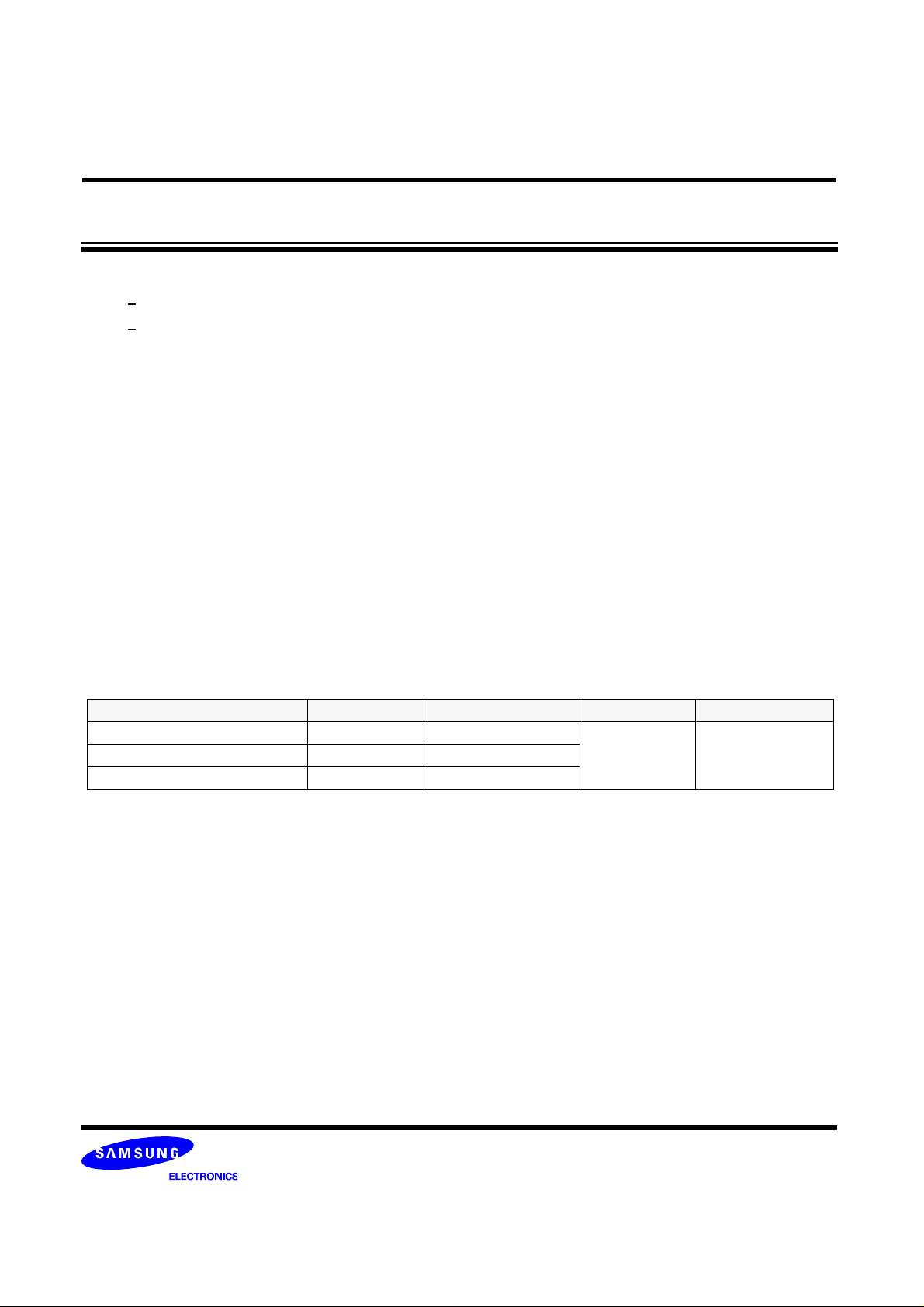
Part NO. Max Freq. Max Data Rate Interface Package
K4D26323RA-GC2A 350MHz 700Mbps/pin
K4D26323RA-GC36 275MHz 550Mbps/pin
SSTL_2
(VDD/VDDQ=2.8V)
144-Ball FBGA K4D26323RA-GC33 300MHz 600Mbps/pin
GENERAL DESCRIPTION
FOR 1M x 32Bit x 4 Bank DDR SDRAM
The K4D26323RA is 134,217,728 bits of hyper synchronous data rate Dynamic RAM organized as 4 x1,048,576 words by
32 bits, fabricated with SAMSUNG’s high performance CMOS technology. Synchronous features with Data Strobe allow
extremely high performance up to 2.8GB/s/chip. I/O transactions are possible on both edges of the clock cycle. Range of
operating frequencies, programmable burst length and pro grammable latencies allow the d evice to be useful for a variety
of high performance memory system applications.
- 4 -
Rev. 2.0 (Jan. 2003)
Page 5
* VDD / VDDQ=2.8V *
K4D26323RA-GC
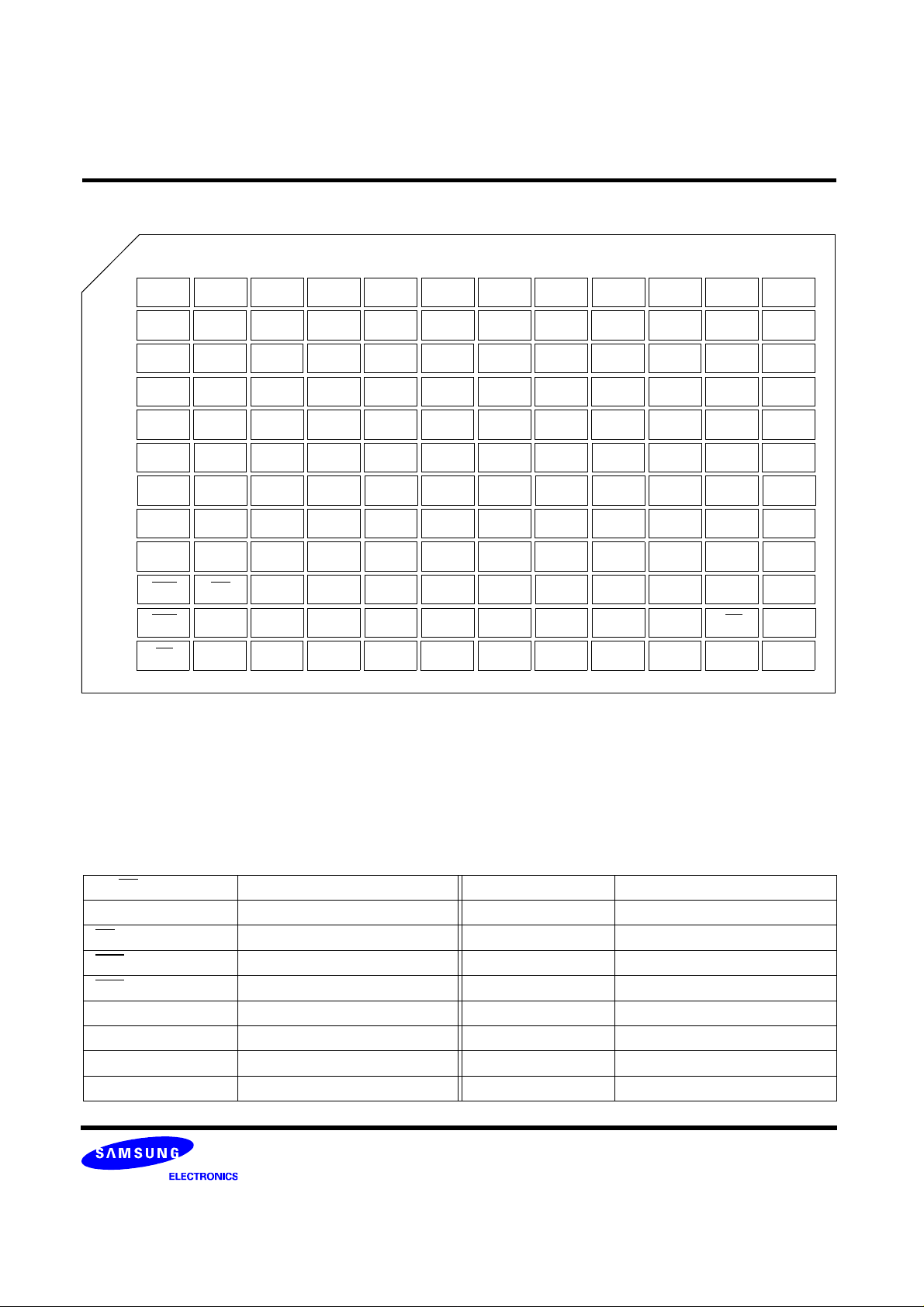
PIN CONFIGURATION (Top View)
2345678910111213
DQS0
B
DM0
VSSQ
DQ3
DQ2
DQ0
DQ31
DQ29
128M DDR SDRAM
DQ28
VSSQ
DM3
DQS3
DQ4
C
DQ6
D
DQ7
E
DQ17
F
DQ19
G
DQS2
H
DQ21
J
DQ22
K
CAS
L
RAS
M
N
CS
VDDQ
DQ5
VDDQ
DQ16
DQ18
DM2
DQ20
DQ23
WE
NC
NC
VSSQ VSSQ VSSQ
VDD
VDDQ
VDDQ
VDDQ
VDDQ
VDD
NOTE:
1. RFU1 is reserved for A12
2. RFU2 is reserved for BA2
3. VSS Thermal balls are optional
NC
NC
NC
BA0
A2
A1
VDDQ
VDD
VSS
Thermal
VSS
Thermal
VSS
Thermal
VSS
Thermal
VDD VDD
A11
A3
VDDQ
VSS VSS VSS VSS
VSSQ
VSSQ
VSSQ
VSSQ
VSSQ
VSS
BA1
A0
DQ1
VSSQ
VSS
Thermal
VSS
Thermal
VSS
Thermal
VSS
Thermal
A10
VDDQ
VDD
VSS
Thermal
VSS
Thermal
VSS
Thermal
VSS
Thermal
A9
A4
DQ30
VSSQ
VSSQ
VSS
Thermal
VSS
Thermal
VSS
Thermal
VSS
Thermal
VSSVSSVSSVSS
RFU
1
A6
VDDQ NC
VSSQ VSSQ
VSSQ
VSSQ
VSSQ
VSSQ
VSSQ
VSS
RFU
A7
VDDQ
DQ26
VDD
VDDQ
VDDQ
NC
VDDQ
VDDQ
VDD
CK
2A5
A8/AP
VDDQ
DQ15
DQ13
DM1
DQ11
DQ9
NC
CK
CKE
DQ27
DQ25
DQ24
DQ14
DQ12
DQS1
DQ10
DQ8
NC
MCL
VREF
PIN DESCRIPTION
CK,CK Differential Clock Input BA0, BA1 Bank Select Address
CKE Clock Enable A0 ~A11 Address Input
CS Chip Select DQ0 ~ DQ31 Data Input/Output
RAS
CAS
WE Write Enable VDDQ Power for DQ’s
DQS Data Strobe VSSQ Ground for DQ’s
DM Data Mask NC No Connection
RFU Reserved for Future Use MCL Must Connect Low
Row Address Strobe VDD Power
Column Address Strobe VSS Ground
- 5 -
Rev. 2.0 (Jan. 2003)
Page 6
* VDD / VDDQ=2.8V *
K4D26323RA-GC
128M DDR SDRAM
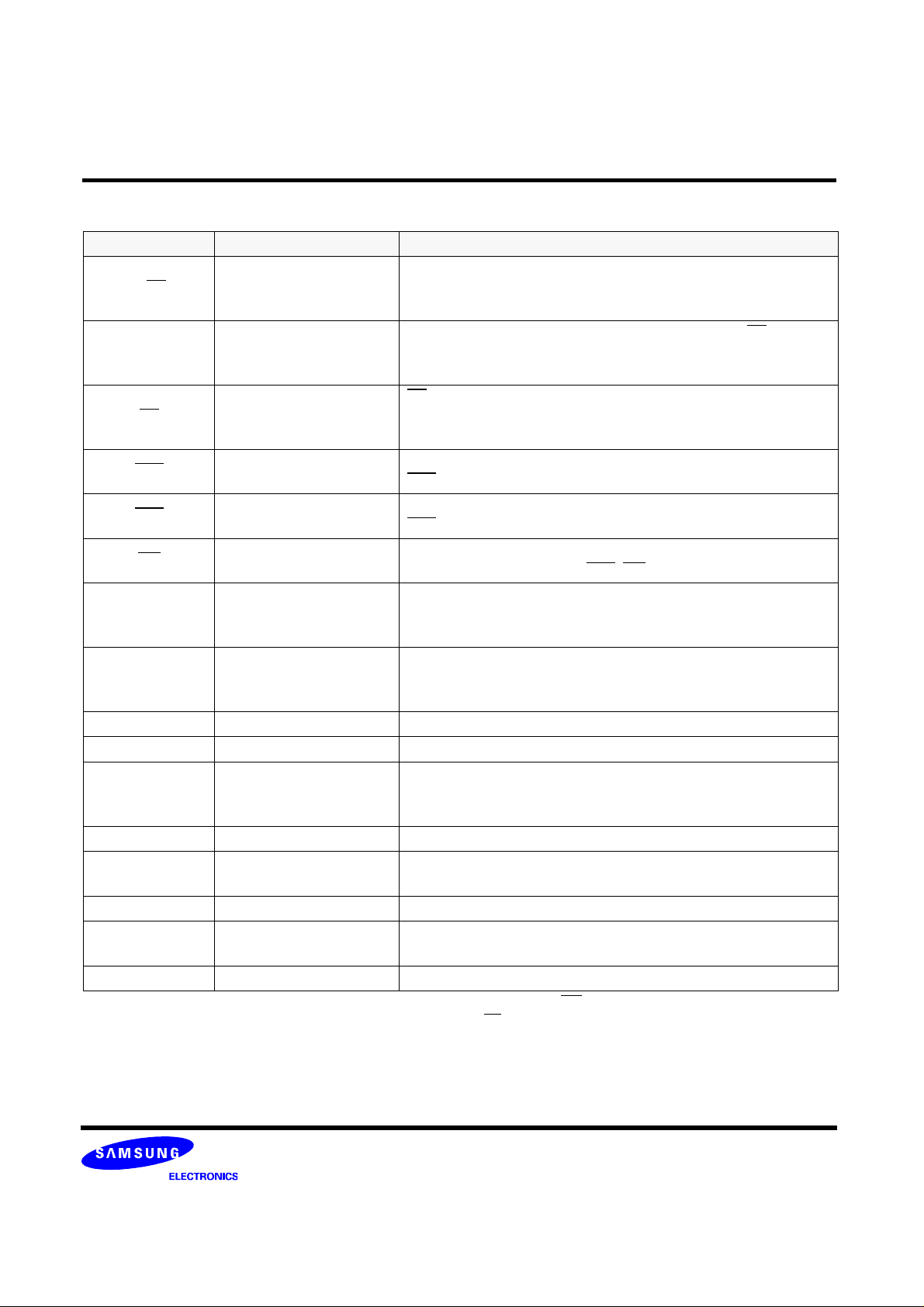
INPUT/OUTPUT FUNCTIONAL DESCRIPTION
Symbol Type Function
The differential system clock Input.
CK, CK*1 Input
CKE Input
CS Input
RAS
CAS Input
WE Input
DQS0 ~ DQS3 Input/Output
DM0 ~ DM3 Input
DQ0 ~ DQ31 Input/Output Data inputs/Outputs are multiplexed on the same pins.
BA0, BA1 Input Selects which bank is to be active.
A0 ~ A11 Input
V
DD/VSS Power Supply Power and ground for the input buffers and core logic.
VDDQ/VSSQ Power Supply
VREF Power Supply Reference voltage for inputs, used for SSTL interface.
NC/RFU No connection/
MCL Must Connect Low Must connect low
*1 : The timing reference point for the differential clocking is the cross point of CK and CK.
For any applications using the single ended clocking, apply V
Input
Reserved for future use
All of the inputs are sampled on the rising edge of the clock except
DQ’s and DM’s that are sampled on both edges of the DQS.
Activates the CK signal when high and deactivates the CK signal
when low. By deactivating the clock, CKE low indicates the Power
down mode or Self refresh mode.
CS enables the command decoder when low an d di sa bl e d th e command decoder when high. When the command decoder is disabled,
new commands are ignored but previous operations continue.
Latches row addresses on the positive going edge of the CK with
RAS
low. Enables row access & precharge.
Latches column addresses on the positive going edge of the CK with
CAS low. Enables column access.
Enables write operation and row precharge.
Latches data in starting from CAS, WE active.
Data input and output are synchronized with both edge of DQS.
DQS0 for DQ0 ~ DQ7, DQS1 for DQ8 ~ DQ15, DQS2 for DQ16 ~ DQ23,
DQS3 for DQ24 ~ DQ31.
Data In mask. Data In is masked by DM Latency=0 when DM is high
in burst write. DM0 for DQ0 ~ DQ7, DM1 for DQ8 ~ DQ15, DM2 for
DQ16 ~ DQ23, DM3 for DQ24 ~ DQ31.
Row/Column addresses are multiplexed on the same pins.
Row addresses : RA0 ~ RA11, Column addresses : CA0 ~ CA7.
Column address CA
Isolated power supply and ground for the output buffers to provide
improved noise immunity.
This pin is recommended to be left "No connection" on the device
REF to CK pin.
8 is used for auto precharge.
- 6 -
Rev. 2.0 (Jan. 2003)
Page 7
* VDD / VDDQ=2.8V *
K4D26323RA-GC
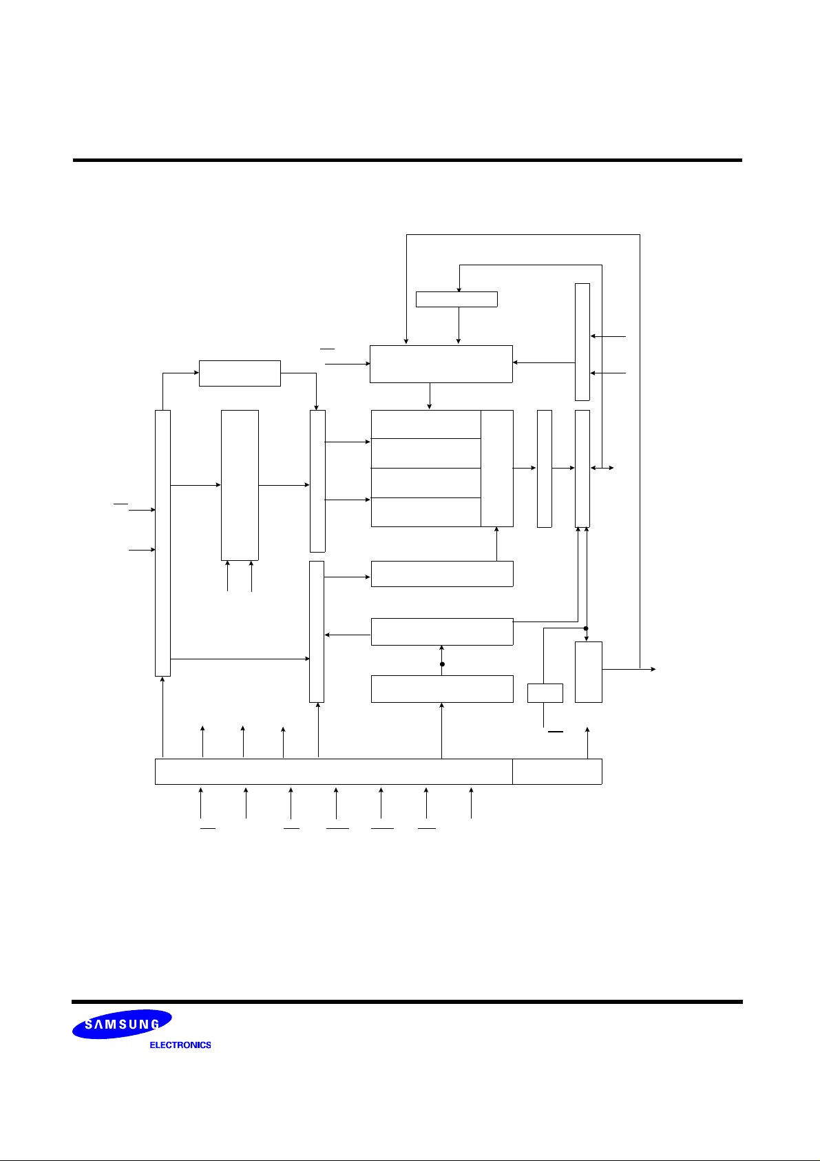
BLOCK DIAGRAM (1Mbit x 32I/O x 4 Bank)
128M DDR SDRAM
32
Intput Buffer
LWE
CK,CK
ADDR
LCKE
Address Register
Bank Select
LRAS
Refresh Counter
Row Buffer
LCBR
LRAS
LCBR
LWE
CK, CK
Row Decoder
Col. Buffer
LCAS
Data Input Register
Serial to parallel
64
1Mx32
1Mx32
1Mx32
1Mx32
Column Decoder
Latency & Burst Length
Programming Register
LWCBR
Sense AMP
2-bit prefetch
64 32
DLL
CK,CK
LDMi
Output BufferI/O Control
x32
DQi
Strobe
Gen.
LDMi
Data Strobe
(DQS0~DQS3)
CK,CK
Timing Register
CKE CS RAS CAS WE DMi
- 7 -
Rev. 2.0 (Jan. 2003)
Page 8
* VDD / VDDQ=2.8V *
K4D26323RA-GC
128M DDR SDRAM
FUNCTIONAL DESCRIPTION
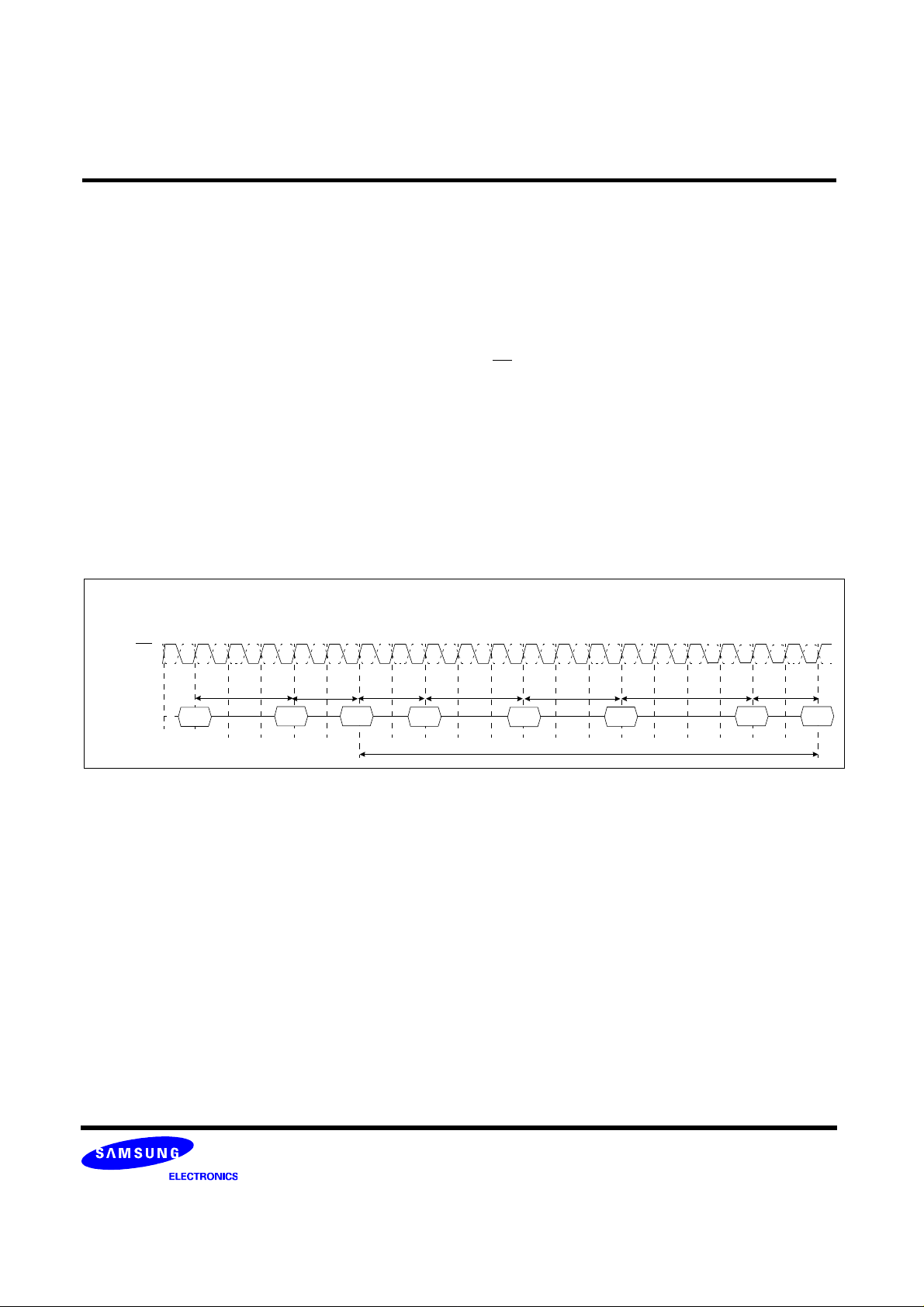
• Power-Up Sequence
DDR SDRAMs must be powered up and initialized in a predefined manner to prevent undefined operations.
1. Apply power and keep CKE at low state (All other inputs may be undefined)
- Apply VDD before VDDQ .
- Apply VDDQ before VREF & VTT
2. Start clock and maintain stable condition for minimum 200us.
3. The minimum of 200us after stable power and clock(CK,CK ), apply NOP and take CKE to be high .
4. Issue precharge command for all banks of the device.
5. Issue a EMRS command to enable DLL
*1 6. Issue a MRS command to reset DLL. The additional 200 clock cycles are required to lock the DLL.
*1,2 7. Issue precharge command for all banks of the device.
8. Issue at least 2 or more auto-refresh commands.
9. Issue a mode register set command with A8 to low to initialize the mode register.
*1 The additional 200cycles of clock input is required to lock the DLL after enabling DLL.
*2 Sequence of 6&7 is regardless of the order.
Power up & Initialization Sequence
0
12345678910111213141516171819
CK,CK
tRP
Command
Inputs must be
stable for 200us
* When the operating frequency is changed, DLL reset should be required again.
After DLL reset again, the minimum 200 cycles of clock input is needed to lock the DLL.
precharge
~
~
ALL Banks
EMRS
2 Clock min.
MRS
DLL Reset
2 Clock min.
precharge
ALL Banks
tRP
1st Auto
Refresh
200 Clock min.
tRFC
~
~
~
~
2nd Auto
~
~
Refresh
~
~
tRFC
~
~
~
~
~
~
Mode
Register Set
2 Clock min.
Any
Command
- 8 -
Rev. 2.0 (Jan. 2003)
Page 9
* VDD / VDDQ=2.8V *
K4D26323RA-GC
128M DDR SDRAM
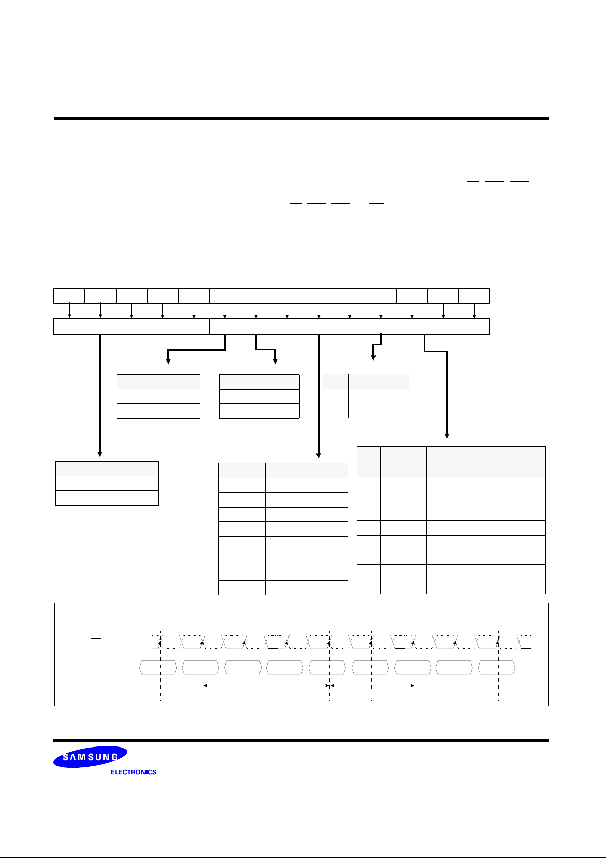
MODE REGISTER SET(MRS)
The mode register stores the data for controlling the various operating modes of DDR SDRAM. It programs CAS latency,
addressing mode, burst length, test mode, DLL reset and various vendor specific opti ons to make DDR SDRAM useful fo r
variety of different applications. The default value of the mode register is not defined, therefore the mode register must be
written after EMRS setting for proper operation. The mod e register is written by asserting low on CS, RAS, CAS and
WE(The DDR SDRAM should be in active mode with CKE already high prior to writing into the mode register). The state of
address pins A0 ~ A11 and BA0, BA1 in the same cycle as CS, RAS, CAS and WE going low is written in the mode register.
Minimum two clock cycles are requested to complete the write operation in the mode register. The mode register contents
can be changed using the same command and clock cycle requirements during operation as long as all banks are in the
idle state. The mode register is divided into various fi elds depending on functionality. The burst length uses A0 ~ A2,
addressing mode uses A3, CAS latency(read latency from column address) uses A4 ~ A6. A7 is used for test mode. A8 is
used for DLL reset. A
for various burst length, addressing modes and CAS latencies.
7,A8, BA0 and BA1 must be set to low for normal MRS operation. Refer to the table for specific codes
BA1 BA0 A11 A10 A9 A8 A7 A6 A5 A4 A3 A2 A1 A0
RFU 0 RFU DLL TM CAS Latency BT Burst Length
DLL
A8 DLL Reset
0No
1Yes
Test Mode
A7 mode
0 Normal
1Test
Burst Type
A3 Type
0 Sequential
1 Interleave
Burst Length
BA0 An ~ A0
0MRS
1EMRS
* RFU(Reserved for future use)
should stay "0" during MRS
cycle.
CAS Latency
A6 A5 A4 Latency
000Reserved
001Reserved
010Reserved
011 3
100 4
101Reserved
110Reserved
111Reserved
A2 A1 A0
Sequential Interleave
0 0 0 Reserve Reserve
001 2 2
010 4 4
011 8 8
1 0 0 Reserve Reserve
1 0 1 Reserve Reserve
1 1 0 Reserve Reserve
1 1 1 Full page Reserve
Address Bus
Mode Register
Burst Type
MRS Cycle
CK, CK
Command
201 534 867
NOP
Precharge
All Banks
NOP
NOP
tRP
*1 : MRS can be issued only at all banks precharge state.
*2 : Minimum
tRP is required to issue MRS command.
- 9 -
NOPMRS NOPNOP
tMRD=2 tCK
Any
Command
Rev. 2.0 (Jan. 2003)
Page 10
* VDD / VDDQ=2.8V *
K4D26323RA-GC
128M DDR SDRAM
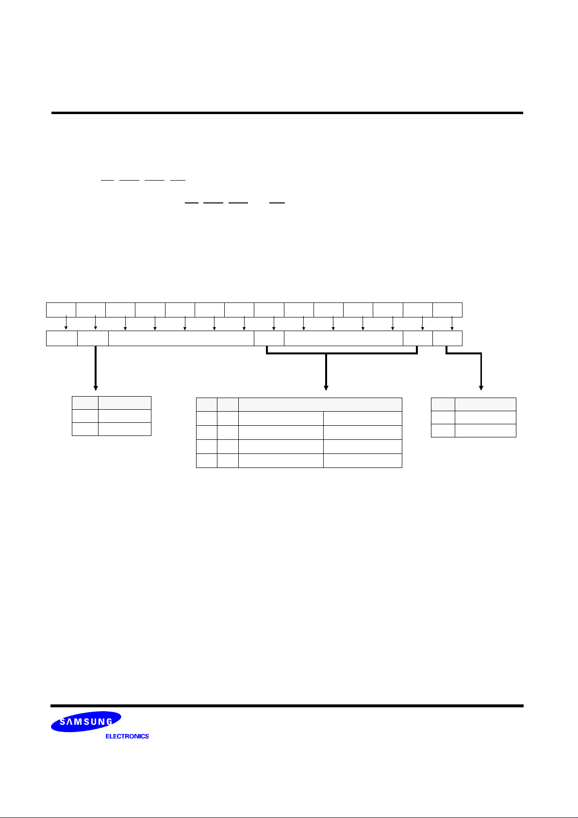
EXTENDED MODE REGISTER SET(EMRS)
The extended mode register stores the data for enabling or disabling DLL and selecting output driver
strength. The default value of the extended mode register is not defined, therefore the extened mode register
must be written after power up for enabling or disabling DLL. The extended mode register is written by asserting low on CS
already high prior to writing into the extended mode register). The stat e of address pins A0, A2 ~ A5 , A7 ~ A11
and BA1 in the same cycle as CS
and A6 are used for setting driver strength to normal, weak or matched impedance. Two clock cycles are
required to complete the write operation in the extended mode register. The mode register contents can be
changed using the same command and clock cycle requirements during operation as long as all banks are in
the idle state. A0 is used for DLL enable or disable. "High" on BA0 is used for EMRS. All the other address
pins except A0,A1,A6 and BA0 must be set to low for proper EMRS operation. Refer to the table for specific
codes.
, RAS, CAS, WE and high on BA0(The DDR SDRAM should be in all bank precharge with CKE
, RAS, CAS and WE going low are written in the extended mode regi ster. A1
1 BA0 A11 A10 A9 A8 A7 A6 A5 A4 A3 A2 A1 A0
BA
RFU 1 RFU D.I.C RFU D.I.C DLL
BA0 An ~ A0
0MRS
1EMRS
*1 : RFU(Reserved for future use) should stay "0" during EMRS cycle.
A6 A1
00
01
10
11
Output Driver Impedence Control
N/A Do not use
Weak 60%
N/A Do not use
N/A Do not use
A0 DLL Enable
0 Enable
1 Disable
Figure 7. Extended Mode Register set
Address Bus
Extended
Mode Register
- 10 -
Rev. 2.0 (Jan. 2003)
Page 11
* VDD / VDDQ=2.8V *
K4D26323RA-GC
128M DDR SDRAM
ABSOLUTE MAXIMUM RATINGS
Parameter Symbol Value Unit
Voltage on any pin relative to Vss V
Voltage on V
Voltage on V
DD supply relative to Vss VDD -1.0 ~ 3.6 V
DD supply relative to Vss VDDQ -0.5 ~ 3.6 V
Storage temperature T
Power dissipation P
Short circuit current I
Note :
Permanent device damage may occur if ABSOLUTE MAXIMUM RATINGS are exceeded.
IN, VOUT -0.5 ~ 3.6 V
STG -55 ~ +150 °C
D 3.3 W
OS 50 mA
Functional operation should be restricted to recommended operating condition.
Exposure to higher than recommended voltage for extended periods of time could affect device reliability.
POWER & DC OPERATING CONDITIONS(SSTL_2 In/Out)
Recommended operating conditions(Voltage referenced to VSS=0V, TA=0 to 65°C)
Parameter Symbol Min Typ Max Unit Note
Device Supply voltage VDD 2.66 2.8 2.94 V 1,7
Output Supply voltage V
Reference voltage V
Termination voltage Vtt V
Input logic high voltage V
Input logic low voltage V
Output logic high voltage V
Output logic low voltage V
Input leakage current I
Output leakage current I
DDQ 2.66 2.8 2.94 V 1,7
REF 0.49*VDDQ - 0.51*VDDQ V2
REF-0.04 VREF VREF+0.04 V 3
IH(DC) VREF+0.15 - VDDQ+0.30 V 4
IL(DC) -0.30 - VREF-0.15 V 5
OH Vtt+0.76 - - V IOH=-15.2mA
OL - - Vtt-0.76 V IOL=+15.2mA
IL -5 - 5 uA 6
OL -5 - 5 uA 6
Note :
1. Under all conditions VDDQ must be less than or equal to VDD.
2. V
REF is expected to equal 0.50*VDDQ of the transmitting device and to track variations in the DC level of the same. Peak to
peak noise on the V
3. V
tt of the transmitting device must track VREF of the receiving device.
4. V
IH(max.)= VDDQ +1.5V for a pulse width and it can not be greater than 1/3 of the cycle rate.
REF may not exceed + 2% of the DC value.
5. VIL(mim.)= -1.5V for a pulse width and it can not be greater than 1/3 of the cycle rate.
6. For any pin under test input of 0V <
7. For K4D26323RA-GC2A/33/36, V
VIN < VDD is acceptable. For all other pins that are not under test VIN=0V.
DD/VDDQ=2.8V + 5%
- 11 -
Rev. 2.0 (Jan. 2003)
Page 12
* VDD / VDDQ=2.8V *
K4D26323RA-GC
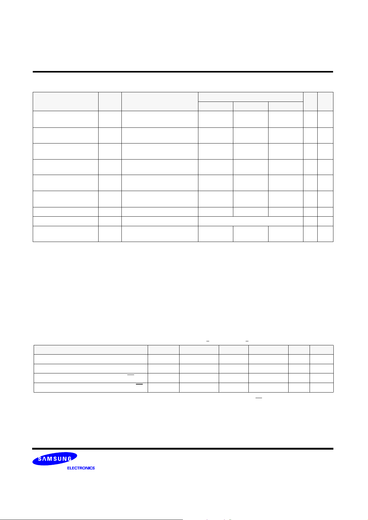
DC CHARACTERISTICS
Recommended operating conditions Unless Otherwise Noted, TA=0 to 65°C)
Parameter Symbol Test Condition
Operating Current
(One Bank Active)
Precharge Standby Current
in Power-down mode
Precharge Standby Current
in Non Power-down mode
Active Standby Current
power-down mode
Active Standby Current in
in Non Power-down mode
Operating Current
( Burst Mode)
Refresh Current I
Self Refresh Current I
Operating Current
(4Bank interleaving)
Note : 1. Measured with outputs open.
2. Refresh period is 32ms.
I
CC1
I
CC2P
CC2N
I
CC3P
I
CC3N
I
CC4
I
CC5
CC6 CKE ≤ 0.2V 4 mA
CC7
I
Burst Lenth=2 tRC ≥ tRC(min)
IOL=0mA, tCC= tCC(min)
CKE
≤ VIL(max), tCC= tCC(min)
CKE ≥ V
tCC= tCC(min)
CKE ≤ V
CKE ≥ VIH(min), CS ≥ VIH(min),
tCC= tCC(min)
IOL=0mA ,tCC= tCC(min),
Page Burst, All Banks activated.
Burst Length=4 tRC ≥ tRC(min)
IOL=0mA, tCC= tCC(min)
IH(min), CS ≥ VIH(min),
IL(max), tCC= tCC(min)
tRC ≥ tRFC(min)
-2A -33 -36
500 480 460 mA 1
85 80 75 mA
145 130 120 mA
140 130 120 mA
400 350 320 mA
940 840 800 mA
330 320 310 mA 2
1200 1080 1000 mA
128M DDR SDRAM
Version
Unit Note
AC INPUT OPERATING CONDITIONS
Recommended operating conditions(Voltage referenced to VSS=0V, VDD=2.8V+ 5%, VDDQ=2.8V+ 5%,TA=0 to 65°C)
Parameter Symbol Min Typ Max Unit Note
Input High (Logic 1) Voltage; DQ VIH VREF+0.4 - - V
Input Low (Logic 0) Voltage; DQ V
Clock Input Differential Volt age; CK and CK
Clock Input Crossing Point Voltage; CK and CK
Note :
1. VID is the magnitude of the difference between the input level on CK and the input level on CK
2. The value of V
IX is expected to equal 0.5*VDDQ of the transmitting device and must track variations in the DC level of the same
IL --VREF-0.4 V
VID 0.8 - VDDQ+0.6 V 1
VIX 0.5*VDDQ-0.2 - 0.5*VDDQ+0.2 V 2
- 12 -
Rev. 2.0 (Jan. 2003)
Page 13
* VDD / VDDQ=2.8V *
K4D26323RA-GC
128M DDR SDRAM
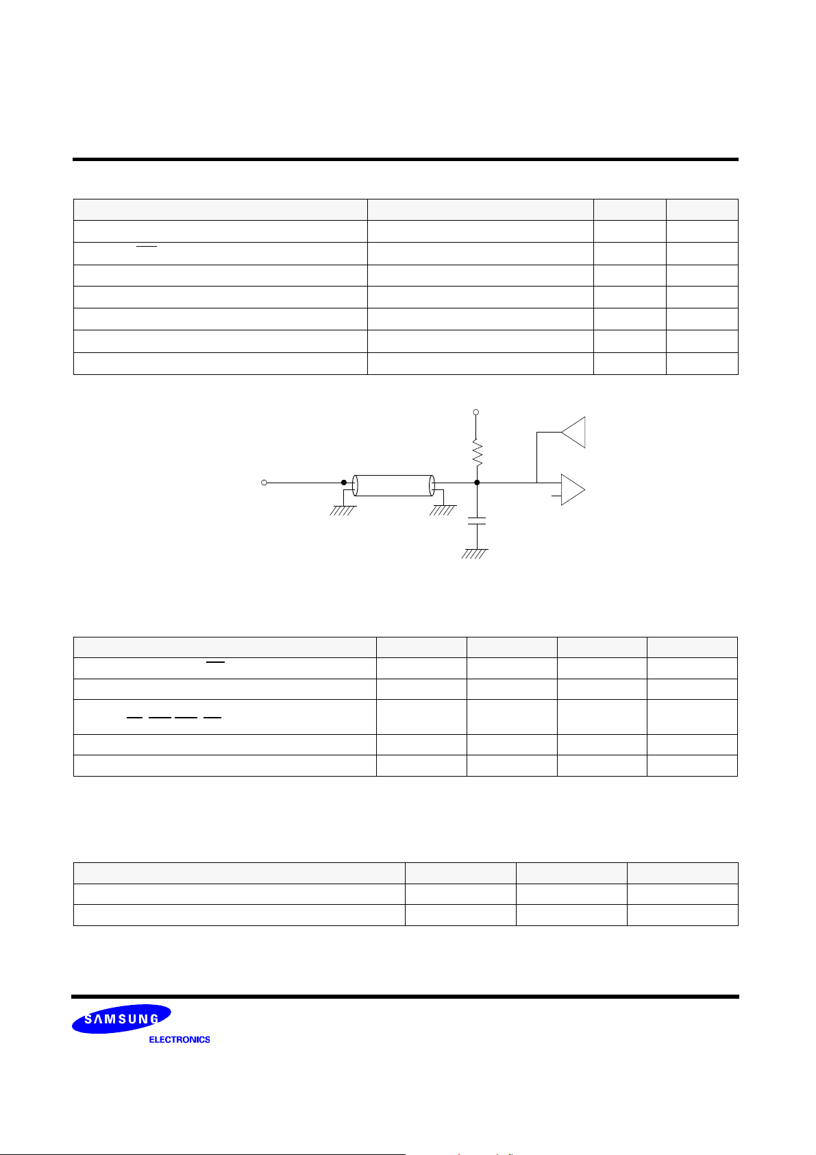
AC OPERATING TEST CONDITIONS (VDD=2.8V±5%, TA= 0 to 65°C)
Parameter Value Unit Note
Input reference voltage for CK(for single ended) 0.50*VDDQ V
CK and CK
CK signal minimum slew rate 1.0 V/ns
Input Levels(VIH/VIL)VREF+0.4/VREF-0.4 V
Input timing measurement reference level VREF V
Output timing measurement reference level Vtt V
Output load condition See Fig.1
signal maximum peak swing 1.5 V
Vtt=0.5*VDDQ
RT=50Ω
Output
Z0=50Ω
C
VREF
=0.5*VDDQ
LOAD=30pF
(Fig. 1) Output Load Circuit
CAPACITANCE (VDD=2.5V, TA= 25°C, f=1MHz)
Parameter Symbol Min Max Unit
Input capacitance( CK, CK )CIN1 1.0 5.0 pF
Input capacitance(A
Input capacitance
(
CKE, CS, RAS,CAS, WE )
Data & DQS input/output capacitance(DQ
Input capacitance(DM0 ~ DM3) C
0~A11, BA0~BA1)CIN2 1.0 4.0 pF
IN3 1.0 4.0 pF
C
0~DQ31)COUT 1.0 6.5 pF
IN4 1.0 6.5 pF
DECOUPLING CAPACITANCE GUIDE LINE
Recommended decoupling capacitance added to power line at board.
Parameter Symbol Value Unit
Decoupling Capacitance between V
Decoupling Capacitance between V
DD and VSS CDC1 0.1 + 0.01 uF
DDQ and VSSQ CDC2 0.1 + 0.01 uF
Note :
1. VDD and VDDQ pins are separated each other.
All V
DD pins are connected in chip. All VDDQ pins are connected in chip.
2. V
SS and VSSQ pins are separated each other
All V
SS pins are connected in chip. All VSSQ pins are connected in chip.
- 13 -
Rev. 2.0 (Jan. 2003)
Page 14
K4D26323RA-GC
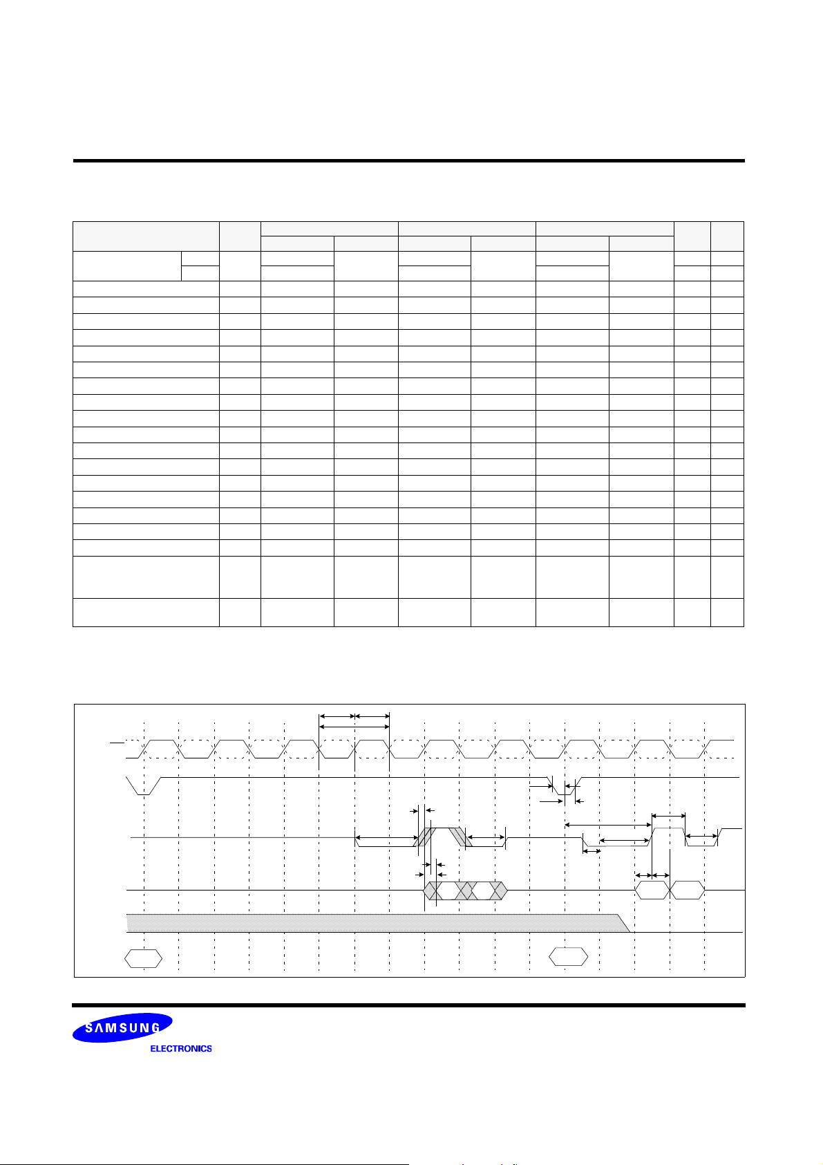
AC CHARACTERISTICS
* VDD / VDDQ=2.8V *
128M DDR SDRAM
Parameter
CK cycle time
CK high level width
CK low level width
DQS out access time from CK
Output access time from CK
Data strobe edge to Dout edge
Read preamble
Read postamble
CK to valid DQS-in
DQS-In setup time
DQS-in hold time
DQS write postamble
DQS-In high level width
DQS-In low level width
Address and Control input setup
Address and Control input hold
DQ and DM setup time to DQS
DQ and DM hold time to DQS
CL=3
CL=4
Sym-
bol
tCK
tCH
tCL
tDQSCK
tAC
tDQSQ
tRPRE
tRPST
tDQSS
tWPRES
tWPREH
tWPST
tDQSH
tDQSL
tIS
tIH
tDS
tDH
-2A -33 -36
Min Max Min Max Min Max
-
2.86 3.3 3.6 ns
0.45 0.55 0.45 0.55 0.45 0.55 tCK
0.45 0.55 0.45 0.55 0.45 0.55 tCK
-0.6 0.6 -0.6 0.6 -0.6 0.6 ns
-0.6 0.6 -0.6 0.6 -0.6 0.6 ns
- 0.35 - 0.35 - 0.40 ns 1
0.9 1.1 0.9 1.1 0.9 1.1 tCK
0.4 0.6 0.4 0.6 0.4 0.6 tCK
0.85 1.15 0.85 1.15 0.85 1.15 tCK
0-0-0-ns
0.35 - 0.35 - 0.35 - tCK
0.4 0.6 0.4 0.6 0.4 0.6 tCK
0.4 0.6 0.4 0.6 0.4 0.6 tCK
0.4 0.6 0.4 0.6 0.4 0.6 tCK
0.9 - 0.9 - 0.9 - ns
0.9 - 0.9 - 0.9 - ns
0.35 - 0.35 - 0.40 - ns
0.35 - 0.35 - 0.40 - ns
tCLmin
Clock half period
tHP
or
tCHmin
Data output hold time from DQS
tQH
tHP-0.35 - tHP-0.35 -
Simplified Timing @ BL=2, CL=4
Unit Note
4
5
tCLmin
-
or
-
tCHmin
-
tCLmin
or
tCHmin
tHP-
0.4
5
ns
-ns1
-ns1
CK, CK
CS
DQS
DQ
DM
COMMAND
01
READA
13467
tCH
tCL
25
tCK
tRPRE
tAC
- 14 -
tDQSCK
tDQSQ
Qa1
tRPST
Qa2
tIS
tIH
WRITEB
tDQSS
tWPREH
tWPRES
tDS
tDH
Db0 Db1
Rev. 2.0 (Jan. 2003)
tDQSH
tDQSL
8
Page 15
* VDD / VDDQ=2.8V *
K4D26323RA-GC
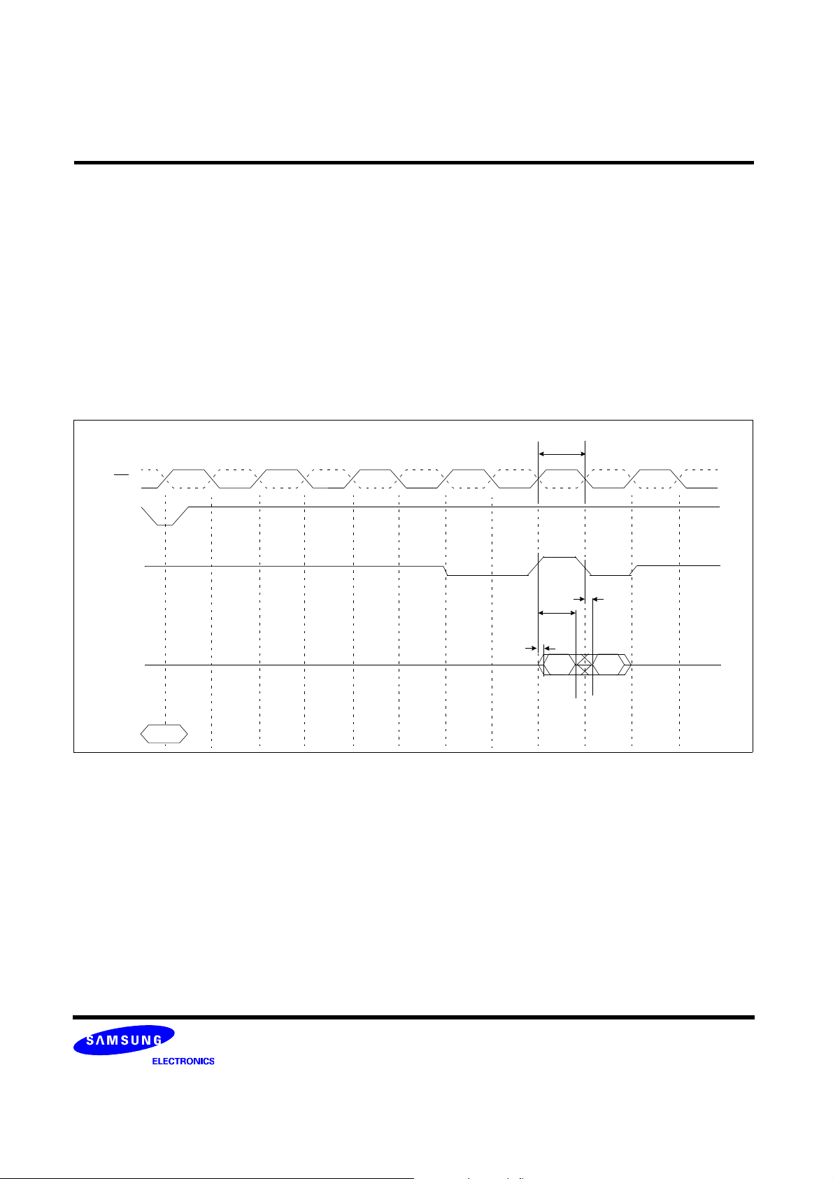
Note 1 :
- The JEDEC DDR specification currently defines the output data valid window(tDV) as the time period when the data
strobe and all data associated with that data strobe are coincidentally valid.
- The previously used definition of tDV(=0.35tCK) artificially penalizes system timing budgets by assuming the worst case
output vaild window even then the clock duty cycle applied to the device is better than 45/55%
- A new AC timing term, tQH which stands for data output hold time from DQS is difined to account for clock duty cycle
variation and replaces tDV
- tQHmin = tHP-X where
. tHP=Minimum half clock period for any given cycle and is defined by clock high or clock low time(tCH,tCL)
. X=A frequency dependent timing allowance account for tDQSQmax
128M DDR SDRAM
tQH Timing (CL4, BL2)
CK, CK
DQS
DQ
COMMAND
CS
01
READA
1
25
3
tDQSQ(max)
tHP
4
tQH
Qa0
tDQSQ(max)
Qa1
- 15 -
Rev. 2.0 (Jan. 2003)
Page 16
* VDD / VDDQ=2.8V *
K4D26323RA-GC
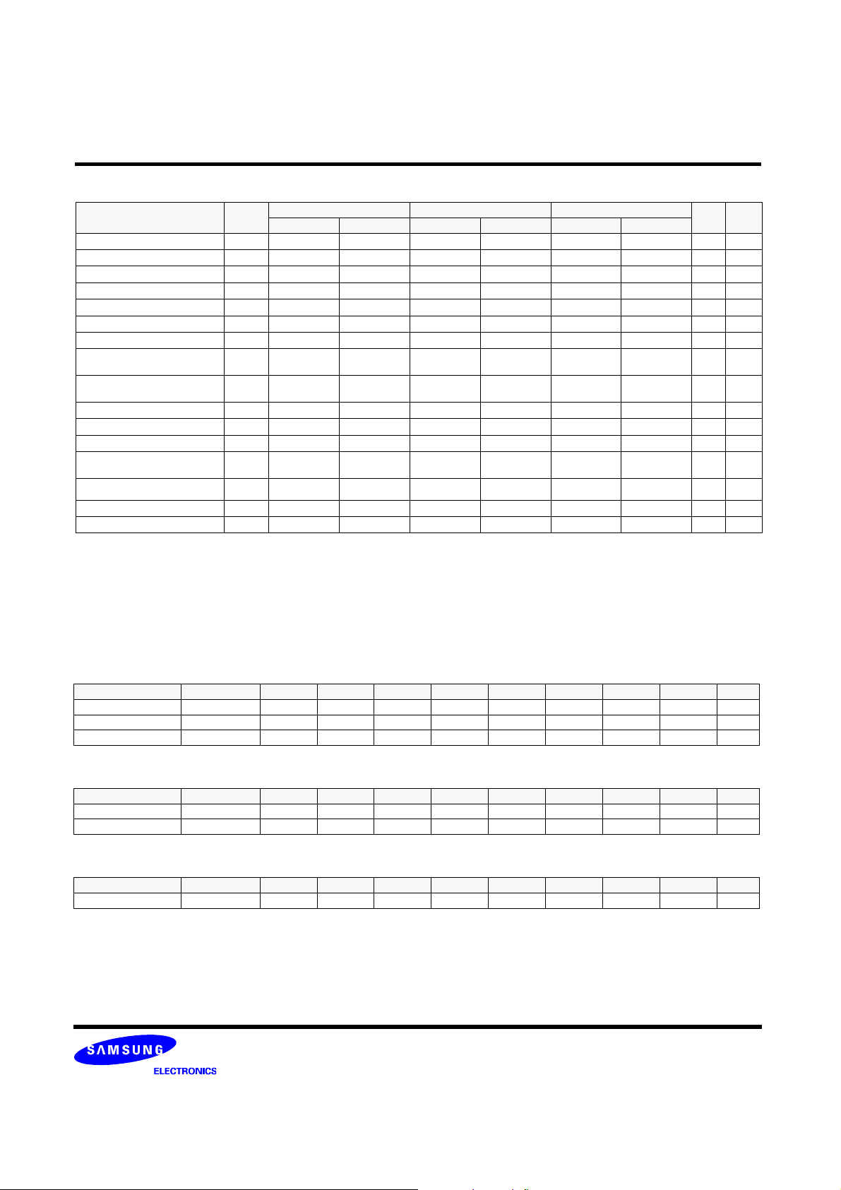
AC CHARACTERISTICS (I)
Parameter
Row cycle time
Refresh row cycle time
Row active time
RAS to CAS delay for Read
RAS to CAS delay for Write
Row precharge time
Row active to Row active
Last data in to Row precharge
@Normal Precharge
Last data in to Row precharge
@Auto Precharge
Last data in to Read command
Col. address to Col. address
Mode register set cycle time
Auto precharge write recovery
+ Precharge
Exit self refresh to read com-
Power down exit time
Refresh interval time
Sym-
bol
tRC
tRFC
tRAS
tRCDRD
tRCDWR
tRP
tRRD
tWR
tWR_A
tCDLR
tCCD
tMRD
tDAL
tXSR
tPDEX
tREF
1tCK+tIS - 1tCK+tIS - 1tCK+tIS - ns
Note : 1. For normal write operation, even numbers of Din are to be written inside DRAM
-2A -33 -36
Min Max Min Max Min Max
15 - 13 -16-tCK
17 - 15 -18-tCK
10 100K 9 100K 11 100K tCK
5 - 4 -5-tCK
323tCK
5 - 4 -5-tCK
4-3-3-tCK
3-2 -3-tCK1
3-3-3-tCK1
2-2-2-tCK1
1-1-1-tCK
2-2-2-tCK
8 - 7 -8-tCK
200 - 200 - 200 - tCK
7.8 - 7.8 - 7.8 - us
128M DDR SDRAM
Unit Note
(Unit : Number of Clock)
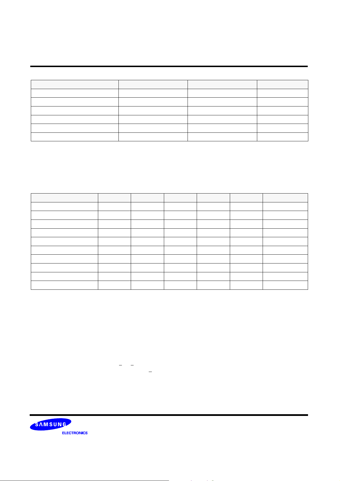
AC CHARACTERISTICS (II)
K4D26323RA-GC2A
Frequency Cas Latency tRC tRFC tRAS tRCDRD tRCDWR tRP tRRD tDAL
350MHz ( 2.86ns ) 41517105354 8 tCK
300MHz ( 3.3ns ) 4 13 15 9 4 2 4 3 7 tCK
275MHz ( 3.6ns ) 4 16 18 11 5 3 5 3 8 tCK
K4D26323RA-GC33
Frequency Cas Latency tRC tRFC tRAS tRCDRD tRCDWR tRP tRRD tDAL
300MHz ( 3.3ns ) 4 13 15 9 4 2 4 3 7 tCK
275MHz ( 3.6ns ) 4 16 18 11 5 3 5 3 8 tCK
K4D26323RA-GC36
Frequency Cas Latency tRC tRFC tRAS tRCDRD tRCDWR tRP tRRD tDAL
275MHz ( 3.6ns ) 4 16 18 11 5 3 5 3 8 tCK
- 16 -
Rev. 2.0 (Jan. 2003)
Unit
Unit
Unit
Page 17
K4D26323RA-GC
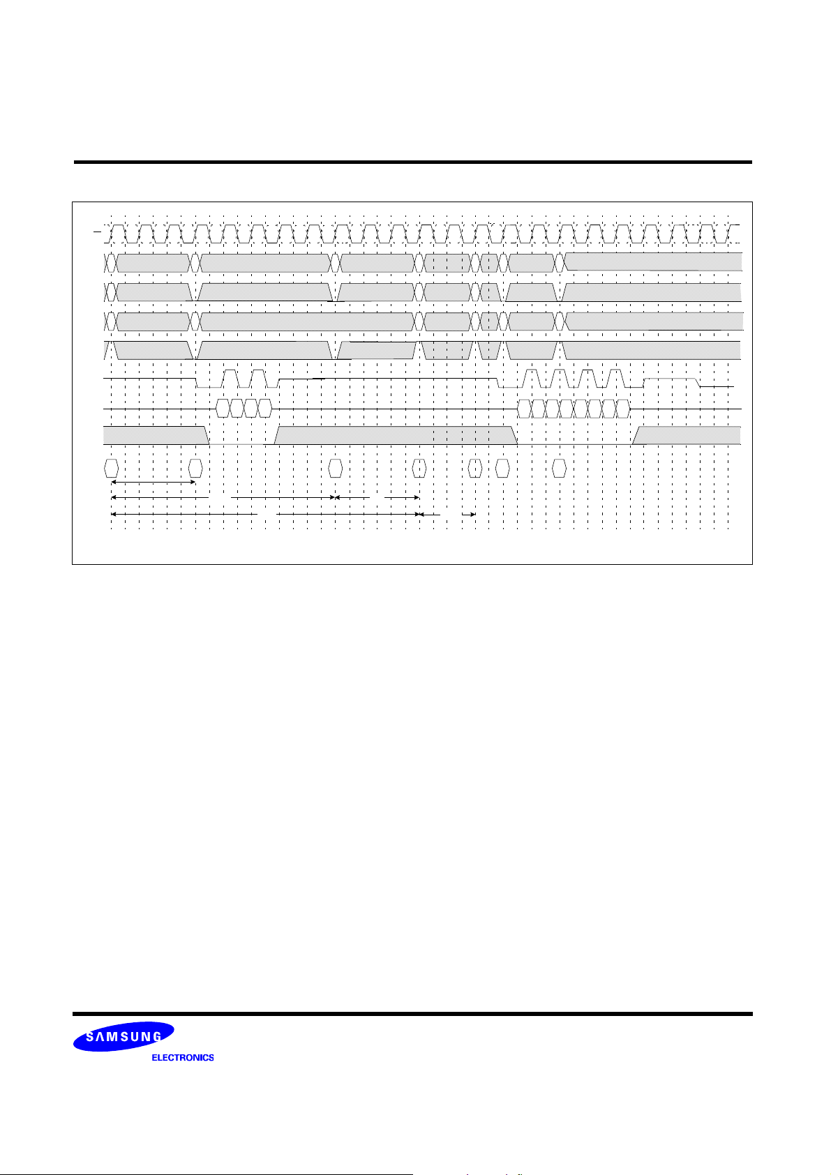
Simplified Timing(2) @ BL=4
* VDD / VDDQ=2.8V *
128M DDR SDRAM
012345678
CK, CK
BA[1:0]
BAa
A8/AP
Ra
Ra
ADDR
(A0~A7,
Ra
A9,A10)
WE
DQS
DQ
DM
COMMAND
ACTIVEA WRITEA
tRCD
BAa
Ca
Da0 Da1 Da2
tRAS
Da3
tRC
Normal Write Burst
(@ BL=4)
BAa
PRECH
9101112
BAa
Ra
Ra
ACTIVEA ACTIVEB WRITEA
BAb
Rb
Rb
tRP
tRRD
Multi Bank Interleaving Write Burst
13 14 15 16 17 18 19 20 21
BAa BAb
Ca
Da0
Cb
Da1 Da2 Da3
WRITEB
Db0 Db1 Db3
Db2
(@ BL=4)
22
- 17 -
Rev. 2.0 (Jan. 2003)
Page 18
* VDD / VDDQ=2.8V *
K4D26323RA-GC
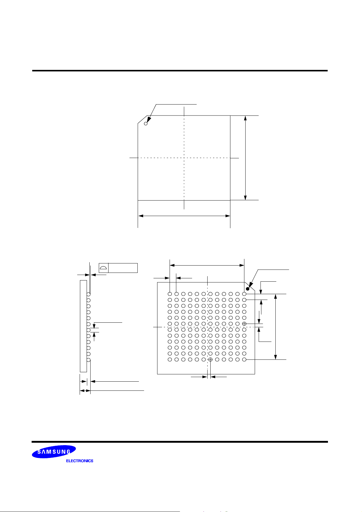
PACKAGE DIMENSIONS (144-Ball FBGA)
A1 INDEX MARK
128M DDR SDRAM
12.0
12.0
0.10 Max
0.45 ± 0.05
0.35 ± 0.05
1.40 Max
<Top View>
0.8x11=8.8
0.8
B
C
D
E
F
G
H
J
K
L
M
N
13 12 11 10 9 8 7 6 5 4 3 2
<Bottom View>
A1 INDEX MARK
0.8
0.8x11=8.8
0.40
0.40
- 18 -
Unit : mm
Rev. 2.0 (Jan. 2003)
 Loading...