

Page 1
UV TO IR DETECTOR
g
g
g
y
)
)
)
)
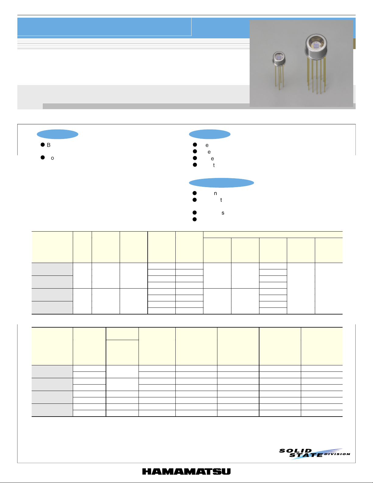
Two-color detector
K1713/K3413-01
,
-02
Broad spectral response range from UV through IR
K1713/K3413-01, -02 detectors have a sandwich structure in which an infrared transmitting silicon photodiode is mounted over an infrared
detector element. This structure allows you to design instruments using the same optical path from UV through IR.
Features
l
Broad spectral response
Suitable for spectrophotometers, flame monitors, etc.
l
Noncooled type:
Room temperature operation for easy handling
One-stage thermoelectrically cooled type:
Keeps the detector temperature at a constant level to
make high-precision measurements.
■
General ratings / Absolute maximum ratings
Dimensi onal
Type No.
K1713-01
K1713-02
K3413-01
K3413-02
outline/
Window
1
material
*
➀
/S TO-5
➁
/S TO-8
Package CoolingDetector
Non-
cooled
One-sta
TE-cooled
e
Si 2.4 × 2.4 5
PbS 1.8 × 1.8 100 *
Si 2.4 × 2.4 5
PbSe 1.8 × 1.8
Si 2.4 × 2.4 5
PbS 1.8 × 1.8 100 *
Si 2.4 × 2.4 5
PbSe 1.8 × 1.8
Applications
l
Spectrophotometers
l
Laser monitors
l
Flame monitors
l
Radiation thermometers
Accessories (Optional)
l
Heatsink for thermoelectrically cooled type A3179-03
l
Temperature controller for thermoelectrically cooled type
l
Photosensor amplifier C2719
l
Amplifier for PbS and PbSe detectors C3757-02
Absolute maximum ratings
Active
area size
(mm) (mW) (A) (V) (°C) (°C)
Thermistor
allowable
dissipation
0.2 1.5
TE-cooler
allowable
current
--
Reverse
volta
V
100 *
100 *
Operating
temper ature
e
R
Topr
2
2
-30 to +50 -55 to +50
2
2
temper ature
C1103-04
Storage
Tstg
■
Electrical and optical characteristics (Typ., unless otherwise noted)
Type No. Detector
K1713-01
K1713-02
K3413-01
K3413-02
*1: Window material S: sapphire glass
*2: Maximum supply voltage
*3: Light source 500 K black body Supply voltage: 15 V
Chopping frequency: 600 Hz, Load resistance: nearly equal to element dark resistance
Noise bandwidth: 60 Hz Input energy: 4.8 µW/cm
*4: l=655 nm
*5: 0 to 63 %
Si 0.94 0.45 300 1.4 × 10
PbS
Si 0.94 0.45 300 1.4 × 10
PbSe
Si 25 0.94 0.45 300 1.4 × 10
PbS -10 2.4 3 × 10⁵ (V/W
Si 25 0.94 0.45 300 1.4 × 10
PbSe -10 4.1 1.5 × 10³ (V/W
Measurement
condition
Element
temperature
T
(°C) (µm) (A/W)
25
25
sensitivity
wavelen
Peak
l
p
2.2 6 × 10⁴ (V/W
4.0 5 × 10² (V/W
Photo sensitivit
th
S
l=l
p
2
(PbSe: 16.7 µW /cm2)
Shunt resistance
or
dark resistance
(MW)
0.2 to 2 5 × 10
0.5 to 1.8 5 × 108 *
0.5 to 10 1 × 10
1.5 to 5 1 × 10⁹ *
(cm · Hz
D*
l=l
p
1/2
10 *3
11 *3
/W)
13
13
3
13
13
3
Rise time
tr
=0 V
R
V
W
=1 k
R
L
10 to 90 %
(µs)
4
0.2 *
200 Max. *
600 Max. *
0.2 *
3 Max. *
0.2 *
0.2 *
5 Max. *
4
4
4
5
5
5
5
1
Page 2
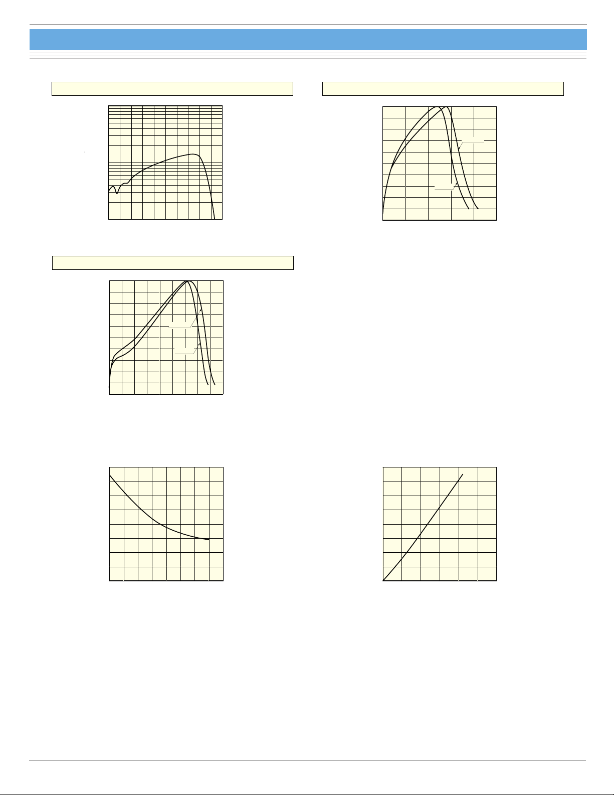
■ Spectral response
(Typ. Ta=25 ˚C, Thermal resistance of heatsink=3 ˚C/W)
VOLTAGE (V)
0
0
1.20.4 0.8 1.00.2 0.6
1.0
0.4
1.6
0.6
0.2
1.4
0.8
1.2
CURRENT (A)
14
10
1
2
13
10
λ
D* (cm · Hz /W)
12
10
0.2
PbSe photoconductive detector
100
80
Two-color detector
K1713/K3413-01, -02
Si photodiode PbS photoconductive detector
WAVELENGTH (µm)
(Typ. Ta=25 ˚C)
(Typ. Ta=25 ˚C)
1.20.4 0.6 0.8 1.0
KIRDB0058EE
100
80
60
40
RELATIVE VALUE (%)
20
0
1
WAVELENGTH (µm)
(Typ. Ta=25 ˚C)
T= -10 ˚C
T=25 ˚C
3.51.5 2 2.5 3
KIRDB0282EA
60
40
RELATIVE VALUE (%)
20
0
1
T= -10 ˚C
T=25 ˚C
45231.5 4.5 5.52.5 3.5
WAVELENGTH (µm)
■ Cooling characteristics of TE-cooler
(Typ. Ta=25 ˚C, Thermal resistance of heatsink=3 ˚C/W)
30
20
10
0
-10
-20
-30
ELEMENT TEMPERATURE (˚C)
-40
-50
0
CURRENT (A)
KIRDB0283EA
■ Current vs. voltage characteristics of TE-cooler
1.61.2 1.40.4 0.8 1.00.2 0.6
2
KIRDB0276EA
KIRDB0277EA
Page 3
Two-color detector
K1713/K3413-01, -02
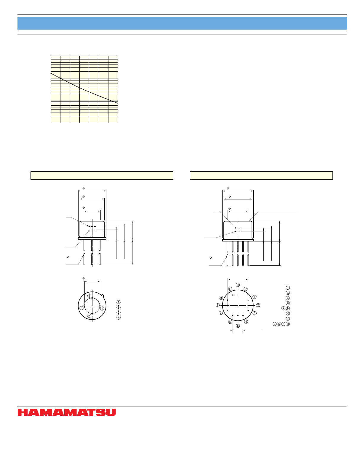
■ Thermistor temperature characteristic
6
10
5
10
4
10
RESISTANCE (Ω)
3
10
-40
ELEMENT TEMPERATURE (˚C)
(Typ.)
30-20 10 20-30 -10 0
KIRDB0278EA
■ Dimensional outline (unit: mm)
➀ K1713-01, -02 ➁ K3413-01, -02
Si
PbS
PbSe
0.4
LEAD
9.2 ± 0.3
8.1 ± 0.2
WINDOW
5.5 ± 0.2
5.1 ± 0.2
3.3 ± 0.2
4.3 ± 0.2
Si (N)
Si (P)
PbS, PbSe
PbS, PbSe
6.1 ± 0.2
30 MIN.
15.3 ± 0.2
14 ± 0.2
WINDOW
10 ± 0.2
Si SAPPHIRE GLASS
PbS
PbSe
0.45
LEAD
6.1 ± 0.2
5.1 ± 0.2
10.0 ± 0.212 MIN.
10.2 ± 0.2
PbS, PbSe
PbS, PbSe
TE-COOLER (-)
TE-COOLER (+)
THERMISTOR
Si (-)
Si (+)
5.1 ± 0.2
KIRDA0041EE KIRDA0043ED
NC
Information furnished by HAMAMATSU is believed to be reliable. However, no responsibility is assumed for possible inaccuracies or omissions.
Specifications are subject to change without notice. No patent rights are granted to any of the circuits described herein. ©2002 Hamamatsu Photonics K.K.
HAMAMATSU PHOTONICS K.K., Solid State Division
1126-1 Ichino-cho, Hamamatsu City, 435-8558 Japan, Telephone: (81) 053-434-3311, Fax: (81) 053-434-5184, http://www.hamamatsu.com
U.S.A.: Hamamatsu Corporation: 360 Foothill Road, P.O.Box 6910, Bridgewater, N.J. 08807-0910, U.S.A., Telephone: (1) 908-231-0960, Fax: (1) 908-231-1218
Germany: Hamamatsu Photonics Deutschland GmbH: Arzbergerstr. 10, D-82211 Herrsching am Ammersee, Germany, Telephone: (49) 08152-3750, Fax: (49) 08152-2658
France: Hamamatsu Photonics France S.A.R.L.: 8, Rue du Saule Trapu, Parc du Moulin de Massy, 91882 Massy Cedex, France, Telephone: 33-(1) 69 53 71 00, Fax: 33-(1) 69 53 71 10
United Kingdom: Hamamatsu Photonics UK Limited: 2 Howard Court, 10 Tewin Road, Welwyn Garden City, Hertfordshire AL7 1BW, United Kingdom, Telephone: (44) 1707-294888, Fax: (44) 1707-325777
North Europe: Hamamatsu Photonics Norden AB: Smidesvägen 12, SE-171 41 Solna, Sweden, Telephone: (46) 8-509-031-00, Fax: (46) 8-509-031-01
Italy: Hamamatsu Photonics Italia S.R.L.: Strada della Moia, 1/E, 20020 Arese, (Milano), Italy, Telephone: (39) 02-935-81-733, Fax: (39) 02-935-81-741
Cat. No. KIRD1029E04
Dec. 2002 DN
3
 Loading...