

Page 1
Copyright & Copy;2000 Shindengen Electric Mfg.Co.Ltd
RATINGS
SHINDENGEN
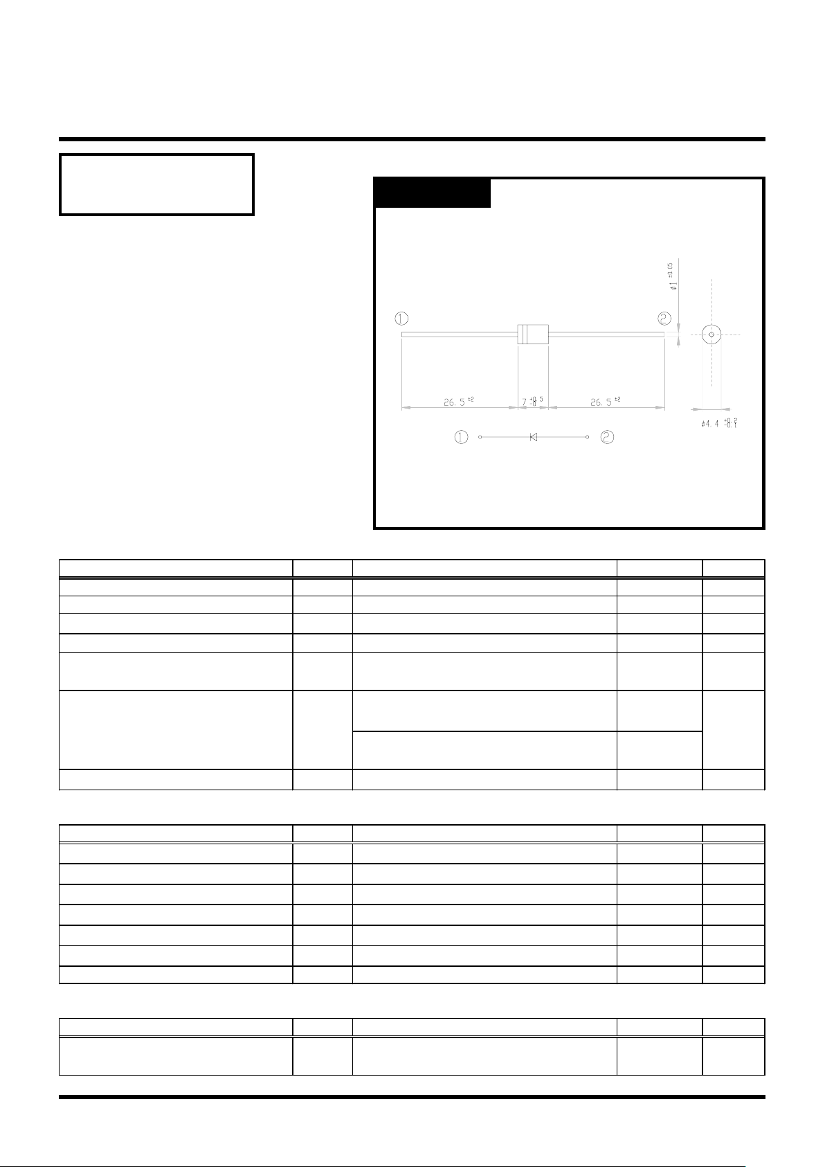
OUTLINE DIMENSIONS
(Unit : mm)
Sidac
K1V36(W)
Case : AX10
●Absolute Maximum Ratings
Item Symbol
Conditions
Ratings Unit
Storage Temperature
Tstg -40~125 ℃
Operating Junction Temperature
Tj 125 ℃
Maximum Off-state Voltage
V
DRM
270 V
RMS On-state Current I
T
Tl = 92℃, 50Hz sine wave (θ = 180°)
1 A
Surge On-state Current
I
TSM
Tj = 25℃, 50Hz sine wave (θ = 180°),
13A
non-repetitive 1-cycle peak value
Ta =25 ℃, pulse width
to = 10 μs, sine wave,
15
Pulse On-state Current
I
TRM
repetitive peak value f = 1 kHz
A
Ta =25 ℃, pulse width to = 10 μs, sine wave,
40
repetitive peak value f = 60 Hz
Critical Rate of Rise of On-state Current
diT/dt 50 A/μs
●Electrical Characteristics (Tl=25℃)
Item Symbol
Conditions
Ratings Unit
Breakover Voltage
V
BO
IB = 0, 50Hz sine wave
340~380 V
Off-state Current
I
DRM
VD = V
DRM
Max 10 μA
Breakover Current
I
BO
Max 0.5 mA
Holding Current
I
H
TYP 50 mA
On-state Voltage
V
T
IT = 1A
Max 3.0 V
Switching Resistance
R
S
Min 0.1 kΩ
Thermal Resistance
θjl
Junction to lead
Max 15 ℃/W
●Standard Design with P.C.B.
Item Symbol
Conditions
Standard Unit
RMS On-state Current
I
T
Assembled in P.C.B., Ta = 25℃,
0.55 A
soldering land 3mmφ
Page 2
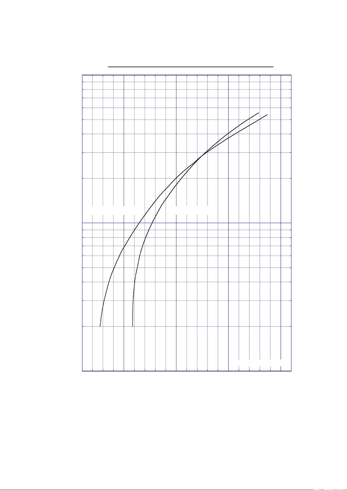
0.1
1
10
2 2.5 3 3.5
K1V33(W)
K1V34(W)
K1V36(W)
K1V38(W)
Pulse measurement
Tl=125°C [TYP] Tl=25°C [TYP]
Instantaneous On-State Voltage VT [V]
Instantaneous On-State Current I
T
[A]
Typical On-State Voltage
Page 3

Power Dissipation
0
0.4
0.8
1.2
1.6
2
2.4
2.8
3.2
0 0.2 0.4 0.6 0.8 1 1.2 1.4
K1V33(W)
K1V34(W)
K1V36(W)
K1V38(W)
Tj=125°C
Sine Wave
Conduction Angle 180°
On-State Current IT (rms) [A]
Power Dissipation P [W]
Page 4

0.1
1
10
100
K1V33(W)
K1V34(W)
K1V36(W)
K1V38(W)
10
-4
10
-3
10
-2
10
-1
10
0
10
1
10
2
10
3
θja
θjl
Transient Thermal Resistance
Duration t [s]
Transient Thermal Resistance θja θjl [°C/W]
Mounted on PCB
20mm
l
Soldering land 3mmφ
l = 2~15mm
Page 5

Breakover Voltage - Junction Temperature
0.85
0.9
0.95
1
1.05
1.1
K1V33(W)
K1V34(W)
K1V36(W)
K1V38(W)
-40 -20 0 20 40 60 80 100 120 140
Junction Temperature Tj [°C]
Breakover Voltage Ratio V
BO
(T) / V
BO
(Tj=25°C)
Page 6

Maximum Lead Temperature
0
0.2
0.4
0.6
0.8
1
1.2
1.4
40 60 80 100 120 140
K1V33(W)
K1V34(W)
K1V36(W)
K1V38(W)
Tj=125°C
Sine Wave
Conduction Angle 180°
Allowable Lead Temperature Tl [°C]
On-State Current I
T
(rms) [A]
Page 7

Maximum Ambient Temperature
0
0.2
0.4
0.6
0.8
1
1.2
0 20 40 60 80 100 120 140
K1V33(W)
K1V34(W)
K1V36(W)
K1V38(W)
Tj=125°C
Sine Wave
Conduction Angle 180°
Allowable Ambient Temperature Ta [°C]
On-State Current I
T
(rms) [A]
Mounted on PCB
20mm
l
Soldering land 3mmφ
l = 2~15mm
Page 8

Maximum Surge On-State Current
0
5
10
15
20
25
30
1 10 100
K1V33(W)
K1V34(W)
K1V36(W)
K1V38(W)
Non-repetitive
Sine Wave 50Hz
Conduction Angle 180°
Free In Air
Tj = 25°C
2 5 20 50
Number of Cycles [cycles]
Surge On-State Current I
TSM
[A]
Page 9

Pulse On-State Current Rating
1
10
100
1000
1 10 100
K1V33(W)
K1V34(W)
K1V36(W)
K1V38(W)
I
P
t
0
1/f
Current Wave Form
Free in air
Sine Wave
Ta = 25°C
0
diT/dt limit line
f = 1 ~ 120Hz
f = 1kHz
f = 5kHz
2 20 50 2005
Pulse Base Width t
0
[µs]
Peak Pulse On-State Current I
P
[A]
Page 10

Pulse On-State Current Derating
0
0.2
0.4
0.6
0.8
1
1.2
0 20 40 60 80 100 120 140
K1V33(W)
K1V34(W)
K1V36(W)
K1V38(W)
I
P
t
0
1/f
Current Wave Form
Free in air
Sine Wave
Ta = 25°C
0
f = 1 ~ 5kHz
f = 1 ~ 120Hz
Ambient Temperature Ta [°C]
Pulse On-State Current Ratio I
P
(T) / I
P
(Ta=25°C)
 Loading...