

Page 1
The JUPITER circuit is designed for use in dual band and dual
mode mobile phones (CDMA/AMPS) and meets the requirements
for IS-95 when used with other chips from Mitel that form the
Planet chipset. JUPITER is an active filter incorporating circuits
for receiving both CDMA and FM (AMPS).
FEATURES
■ Low Power and Low Voltage Operation with a
Sleep Mode
■ Integrated CDMA and FM Filter with Wide
Dynamic Range
■ Low Inband Gain Ripple Performance and Good
I/Q Matching for the Filter
ABSOLUTE MAXIMUM RATINGS
Supply voltage, V
Operating temperature, T
Storage temperature, T
Junction temperature
CMOS input logic high, V
CMOS input logic low, V
Maximum input voltage at all pins
CC MAX
OP
(ambient)
STG
IH
IL
(at pins)
ORDERING INFORMATION
JUPITER-1/KG/NP1S
20·6V to V
20·7V to 15·3V
230°C to170°C
240°C to 1150°C
230°C to 1125°C
V
10·6V (Max.)
CC
20·6V (Min.)
10·6V
CC MAX
JUPITER
CDMA and FM (AMPS) I/Q Filter
Preliminary Information
DS4724 - 3.1 May 1998
Q_OC_TEST
Q_OC_TESTB
QIN
QINB
Q_OFFSET
Q_OFFSETB
V
TEST
RTUNE
ITUNE
QTUNE
QBAL
QOUT
QOUTB
V
CC
1
2
3
4
5
6
7
JUPITER
8
9
10
11
12
13
14
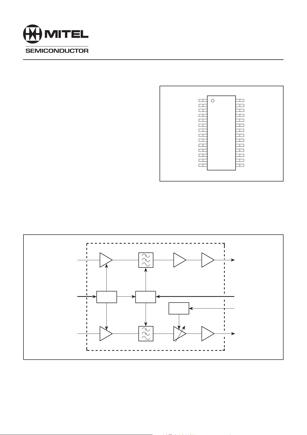
Fig. 1 Pin connections - top view
ESD PROTECTION
All pins are protected against electrostatic discharge to both
supplies. At least 2kV protection is provided to MIL-STD-883D
Method 3015.7 (human body model).
28
27
26
25
24
23
22
21
20
19
18
17
16
15
I_OC_TEST
I_OC_TESTB
IIN
IINB
I_OFFSET
I_OFFSETB
V
EE
MODE_CDMA
ENABLE
ENTEST
V
REF
IOUT
IOUTB
2
V
EE
NP28
IIN
MODE
SELECT
INPUTS
QIN
MODE
CONTROL
I CHANNEL
FILTER
CONTROL
GAIN
CONTROL
Q CHANNEL
Fig. 2 Simplified block diagram
IOUT
TUNE
CONTROLS
V
GC
QBAL
QOUT
Page 2
JUPITER
CIRCUIT DESCRIPTION
The block diagram of the JUPITER filter is shown in
Fig. 3. Two tunable active low-pass gyrator filters are designed
with balanced I/Q inputs and outputs.
CDMA MODE
In CDMA mode the filter (F1 on Fig. 3) is a 7th order 0.1dB
ripple continuously tunable elliptic type with the corner frequency
tuned to 690kHz for best stop band attenuation and minimal
phase error (in the overall system). Variable gain stages after the
filter provide the gain control capability. Overall, each of the
CDMA I/Q channels has 45dB nominal voltage gain with the Q
channel having ±2dB gain adjustment range. Separate I/Q
frequency tuning functions are built into the device.
FM MODE
In FM mode the same filter is used; however, the biasing is
designed such that the current density in the transconductor cells
is reduced by a factor of 46, changing the filter’s cutoff frequency
to 15kHz. The filter characteristic of the main channel filter
(gyrator filter) remains the same, i.e. a 0.1dB 7th order elliptic. In
FM mode additional 2nd order Sallen and Key 0.1dB ripple
Chebeyshev filters (F2) are included in the signal path prior to the
gyrators. These improve the out-of-band blocking of the overall
filter. Different amplifiers are used in FM mode to those used in
CDMA mode to enable optimization of the gain distribution in FM
mode for current consumption and dynamic range.
OPERATION
Signal inputs are DC coupled in both CDMA and FM modes.
The device modes are selected by CMOS compatible logic
signals as shown in Table 2. An external resistor should be
connected between RTUNE and ground to set internal currents;
a resistor with a tolerance of 65% and a temperature coefficient
of less than 100ppm is recommended. V
(pin 18) should be
REF
decoupled to VCC to give optimum supply rejection.
A test mode is provided for filter calibration. In this mode, a test
signal is applied to the V
input (pin 7) with ENTEST held high.
TEST
The test mode is designed to interface with the PLUTO baseband
processor, which can provide the test signal and I/QTUNE
voltages and calibrates the filters using an internal auto calibration
algorithm. The algorithm generates two test frequencies and
calibrates the filters to give the correct attenuation at the upper
frequency. The calibration is normally carried out in CDMA
mode: the FM filter performance is scaled accordingly.
Pins are provided for DC offset control for I and Q channels
(I_OFFSET, I_OFFSETB, Q_OFFSET and Q_OFFSETB). In
typical operation, the I_OFFSET/Q_OFFSET pins would be
controlled by a voltage derived from the baseband processor.
However, it is also possible to minimise the DC offset using
external components; this is primarily intended for test purposes.
These feedback components between IOUT/QOUT and
I_OFFSET/Q_OFFSET are shown in Fig. 4 but would not be
used in the normal application
In test mode, these offset controls are disabled and the offsets
are controlled using on-chip feedback. The loop filter for this
feedback uses external 10nF capacitors on pins I_OC_TEST/B
and Q_OC_TEST/B as shown in Fig. 4.
Pin
Q_OC_TEST
1
Q_OC_TESTB
2
QIN
3
QINB
4
Q_OFFSET
5
Q_OFFSETB
6
V
7
8
RTUNE
9
ITUNE
10
QTUNE
11
QBAL
12
QOUT
13
QOUTB
14
V
15
VEE2
16
IOUTB
17
IOUT
18
V
19
ENTEST
20
ENABLE
21
MODE_CDMA
22
V
23
I_OFFSETB
24
I_OFFSET
25
IINB
26
IIN
27
I_OC_TESTB
28
I_OC_TEST
TEST
CC
REF
EE
Name
I/O
Q channel offset control in test mode
I
Q channel offset control in test mode (balanced)
I
Q channel CDMA/FM input.
I
Q channel CDMA/FM input (balanced)
I
Q channel offset control
I
Q channel offset control (high gain mode)
I
Test mode signal input for tuning operation
I
Description
Precision resistor for current definition (18k)
I filter tuning control
I
Q filter tuning control
I
Q channel gain adjust voltage, VGC
I
Q channel CDMA/FM output
O
Q channel CDMA/FM output (balanced)
O
Supply
P
Ground
P
I channel CDMA (balanced)
O
I channel CDMA
O
Reference voltage decouple
Mode control (see Table 2)
I
Mode control (see Table 2)
I
Mode control (see Table 2)
I
Ground (substrate)
P
I channel offset control (high gain mode)
I
I channel offset control
I
I channel CDMA (balanced)
I
I channel CDMA
I
I channel offset control in test mode (balanced)
I
I channel offset control in test mode
I
Table 1 Pin descriptions
2
Page 3
Q_OFFSET
Q_OFFSETB
JUPITER
Q_OC_TESTBQ_OC_TEST
12
5
6
-0·1
dB
gm
gm
Q CHANNEL
± 2dB
F2
gm
50k
F3
V
GC
11
QBAL
QIN
QINB
ENTEST
ENABLE
MODE_CDMA
V
TEST
IIN
IINB
I_OFFSET
I_OFFSETB
3
-0·1
dB
ATTENUATOR
ATTENUATOR
F2
gm
4
19
20
21
7
26
25
24
23
MODE
CONTROL
gm
gm
gm
gm
F1
FILTER
CONTROL
F1
gm
F3
50k
28 27
I_OC_TESTBI_OC_TEST
X1
X1
12
13
10
8
9
17
16
15
22
14
18
QOUT
QOUTB
QTUNE
RTUNE
ITUNE
IOUT
IOUTB
VEE2
V
EE
V
CC
V
REF
Description ENTEST
ENABLE
Sleep mode
CDMA mode
FM mode
CDMA filter testmode
FM filter test mode
Disallowed mode
MODE_
CDMA
0
1
1
1
1
0
X
1
0
1
0
X
Fig. 3 Block diagram
All circuits powered down
1
Biasing and CDMA signal path on
0
Biasing and FM signal path on
0
Biasing, CDMA test and CDMA signal path on, excluding input amplifier
1
Biasing, FM test and FM signal path on, excluding input amplifier.
1
This is functionally the same as sleep mode but has higher I
0
In sleep mode PLUTO applies a logic high to ENTEST
Table 2 Truth table for mode control lines
Comments
CC
.
3
Page 4

JUPITER
ELECTRICAL CHARACTERISTICS
The Electrical Characteristics are guaranteed over the following range of operating conditions unless otherwise
stated (see Fig. 4 for test circuit):
T
= 2 30°C to 170°C, VCC = 3V 10·6V/20·3V
AMB
DC Characteristics
Value
Characteristic Conditions
General
Supply voltage, V
Operating temperature, T
CC
AMB
Min.
2·7
230
Typ.
3·0
Max.
3·6
170
Units
V
°C
Supply Current, I
Sleep mode
FM mode
CDMA mode
Turn off time, CDMA/FM
mode to Sleep mode
Mode Control Lines (CMOS)
Input logic high, V
Input logic low, V
Input high current I
Input low current, I
Tune/Gain Control Lines
DC level
Input impedances:
QBAL, ITUNE and QTUNE
I_OFFSET/B and Q_OFFSET/B
I/O DC Voltages
Inputs IIN/B and QIN/B
Outputs IOUT/B and QOUT/B
CC
IH
IL
IH
IL
V
V
2·0
20·1
220
220
0·5
CC
CC
20·6
21·6
0·15
V
V
V
5·2
11·0
CC
0·5
20
20
2·0
CC
CC
10·1
20·2
21·2
3·4
7·3
100
200
500
V
20·4
CC
V
21·4
CC
mA
mA
mA
µA
µA
kΩ
kΩ
QBAL = ITUNE = QTUNE <0·5V
QBAL = ITUNE = QTUNE = 1·2V
QBAL = ITUNE = QTUNE = 1·2V
I
µs
V
V
reduced to 10% of active value
CC
All logic inputs
%
V
Referenced to on-chip ref. voltage (1·2V)
V
V
4
Page 5

ELECTRICAL CHARACTERISTICS
FM Mode AC Characteristics
All parameters are defined as differential unless otherwise stated
Value
Characteristic Conditions
Min.
Typ.
JUPITER
Units
Max.
Maximum input frequency
Gain Characteristics
I voltage gain (A
Q voltage gain QIN/B to QOUT/B
Q channel gain adjust
Q channel gain control
Gain variation over temperature and
supply voltage
Differential output amplitude balance,
QOUT/QOUTB, IOUT/IOUTB
Power Supply Rejection
In-band
Out of band
Noise
Input referred
1dB Compression
Output 1dB compression
Out of band blocking signal causing 1dB
compression of in-band signal
Blocking signal at 60kHz
Blocking signal at 120kHz
) IIN/B to IOUT/B
V
39
21·5
A
V
62
20·75
1·5
266
266
41
4·0
10
0
30
1·9
380
380
10
43
11·5
A
V
8·0
10·75
60·25
45
MHz
dB
dB
dB/V
dB
dB
dB
dB
µVrms
Vp-p
mVrms
mVrms
mVrms
mVrms
External load = 50kΩ//5pF
QBAL = 1·2V
QBAL = 0·5 to 2V
= 6150mV
V
CC
Measured at I/Q output frequency = 10kHz
Measured at I/Q output frequency = 630kHz
Bandwidth = 10Hz to 5MHz. I and Q channels
Frequency = 2kHz
In-band frequency = 2kHz. All conditions
27°C only
In-band frequency = 2kHz. All conditions
27°C only
Intermodulation
Input referred intermodulation product
Filter Characteristic (Note 1)
3dB pass band
Stop band attenuation 45kHz
Stop band attenuation 60kHz to 10MHz
I and Q bandwidth matching
In-band gain ripple
Group delay variation
Average phase balance, I and Q channels
Offset Loop Correction
Filter offset adjustment gain:
I_OFFSET/Q_OFFSET
I_OFFSET B/Q_OFFSETB
Amplifier offset settling time:
After power on
After CDMA to FM cycling
Input Impedances
QIN/QINB and IN/INB
Output Impedances
QOUT/QOUTB and IOUT/IOUTB
14·5
48
60
0·6
8·0
2101
8·8
16·5
63
70
30
1·0
10
4·0
10
1·0
19·5
5
1·0
10
1·4
4·0
12
dBV
µVrms
kHz
dB
dB
%
dBp-p
µs
deg
V/V
V/V
ms
ms
kΩ
kΩ
Unmodulated interferers
60kHz 75mVrms, 120kHz 7·5mVrms
ITUNE = QTUNE = 1·2V
Frequency = 100Hz to 12·2kHz
%
Settling to within 5mV
Settling to within 5mV
Frequency = 2kHz
Frequency = 2kHz
NOTE 1. Filter tuned in CDMA mode to 28dB at 720kHz
5
Page 6

JUPITER
ELECTRICAL CHARACTERISTICS
CDMA Mode AC Characteristics
All parameters are defined as differential unless otherwise stated
Value
Characteristic Conditions
Min.
Typ.
Max.
Units
Maximum input frequency
Gain Characteristics
I voltage gain (A
) IIN/B to IOUT/B
V
Q voltage gain QIN/B to QOUT/B
Q channel gain adjust
Q channel gain control
Gain variation over temperature and
supply voltage
Differential output amplitude balance,
QOUT/QOUTB, IOUT/IOUTB
Power Supply Rejection
In-band
Noise
Input referred
1dB Compression
Output 1dB compression
Out of band blocking signal causing 1dB
compression of in-band signal
Blocking signal at 60kHz
Blocking signal at 120kHz
43
21·5
A
V
62
20·75
1·5
110
110
45
4·0
20
110
1·9
150
150
10
47
AV11·5
8·0
10·75
60·25
MHz
dB
dB
dB/V
dB
dB
dB
µVrms
Vp-p
mVrms
mVrms
mVrms
mVrms
External load = 50kΩ//5pF
QBAL = 1·2V
QBAL = 0·5 to 2V
= 6150mV
V
CC
Measured at I/Q output frequency = 690kHz
Bandwidth = 10Hz to 5MHz. I and Q channels
Frequency = 2kHz
In-band frequency = 100kHz. All conditions
27°C only
In-band frequency = 100kHz. All conditions
27°C only
Intermodulation
Input referred intermodulation product
Input referred intermodulation product
2101
8·8
2101
8·8
284·8
57
284·8
57
dBV
µVrms
dBV
µVrms
dBV
µVrms
dBV
µVrms
Unmodulated interferers
900kHz 24mVrms, 1700kHz 15mVrms
27°C only
Unmodulated interferers
1·25MHz 24mVrms, 2·25MHz 15mVrms
27°C only
Filter Characteristic (Note 1)
ITUNE/QTUNE voltage
0·5
1·2
2·0
Tuning voltage to set filter to 28dB
V
at 720kHz relative to 350kHz
Pass band variation over supply and
23
13
0
%
V
CC
= 6150mV
temperature variation
I/Q tuning gain
Stop band attenuation 900kHz to 10MHz
50
240
55
I and Q bandwidth matching
In-band gain ripple
1·0
Average phase balance, I and Q channels
NOTE 1. Filter tuned to 28dB at 720kHz relative to 350kHz Cont…
kHz/V
dB
4
dBp-p
3
deg
ITUNE = QTUNE = 1·2V
%
Frequency = 1kHz to 630kHz
Frequency = 1kHz to 630kHz
6
Page 7

ELECTRICAL CHARACTERISTICS
CDMA Mode AC Characteristics (continued)
Characteristic Conditions
Offset Loop Correction
Filter offset adjustment gain:
I_OFFSET/Q_OFFSET
I_OFFSET B/Q_OFFSETB
Amplifier offset settling time:
After power on
After FM to CDMA cycling
Input Impedances
QIN/QINB and IN/INB
Output Impedances
QOUT/QOUTB and IOUT/IOUTB
Min.
1·2
8·0
Value
Typ.
2·0
2·0
10
1·0
Max.
2·8
10
4·0
12
Units
V/V
V/V
ms
ms
kΩ
kΩ
JUPITER
Settling to within 6mV
Settling to within 6mV
Frequency = 2kHz
Frequency = 2kHz
V
CC
QTUNE
QIN
QIN
QINB
Q_OFFSET
10n 10n
QOUT
100n
V
CC
100k100k
10n 10n
Q_OFFSETB
Q_OC_TEST
Q_OC_TESTB
QOUT
V
QBAL MODE_CDMA
EN_TEST ENABLE
TEST
JUPITER
IINB
I_OFFSET
I_OFFSETB
I_OC_TEST
I_OC_TESTB
IOUT
IIN
ITUNE
100n
100k100k
V
CC
IIN
IOUT
QOUTB
RTUNE
220n 18k
VEEVEE2
Fig. 4 Test circuit
1n
V
REF
IOUTB
100n
V
CC
7
Page 8

Page 9

http://www.mitelsemi.com
World Headquarters - Canada
Tel: +1 (613) 592 2122
Fax: +1 (613) 592 6909
North America Asia/Pacific Europe, Middle East,
Tel: +1 (770) 486 0194 Tel: +65 333 6193 and Africa (EMEA)
Fax: +1 (770) 631 8213 Fax: +65 333 6192 Tel: +44 (0) 1793 518528
Fax: +44 (0) 1793 518581
Information relating to products and services furnished herein by Mitel Corporation or its subsidiaries (collectively “Mitel”) is believed to be reliable. However, Mitel assumes no
liability for errors that may appear in this publication, or for liability otherwise arising from the application or use of any such information, product or service or for any infringement of
patents or other intellectual property rights owned by third parties which may result from such application or use. Neither the supply of such information or purchase of product or
service conveys any license, either express or implied, under patents or other intellectual property rights owned by Mitel or licensed from third parties by Mitel, whatsoever.
Purchasers of products are also hereby notified that the use of product in certain ways or in combination with Mitel, or non-Mitel furnished goods or services may infringe patents or
other intellectual property rights owned by Mitel.
This publication is issued to provide information only and (unless agreed by Mitel in writing) may not be used, applied or reproduced for any purpose nor form par t of any order or
contract nor to be regarded as a representation relating to the products or services concerned. The products, their specifications, services and other information appearing in this
publication are subject to change by Mitel without notice. No warranty or guarantee express or implied is made regarding the capability, performance or suitability of any product or
service. Information concerning possible methods of use is provided as a guide only and does not constitute any guarantee that such methods of use will be satisfactory in a specific
piece of equipment. It is the user’s responsibility to fully determine the performance and suitability of any equipment using such information and to ensure that any publication or
data used is up to date and has not been superseded. Manufacturing does not necessarily include testing of all functions or parameters. These products are not suitable for use in
any medical products whose failure to perform may result in significant injury or death to the user. All products and materials are sold and services provided subject to Mitel’s
conditions of sale which are available on request.
M Mitel (design) and ST-BUS are registered trademarks of MITEL Corporation
Mitel Semiconductor is an ISO 9001 Registered Company
Copyright 1999 MITEL Corporation
All Rights Reserved
Printed in CANADA
TECHNICAL DOCUMENTATION - NOT FOR RESALE
 Loading...