

Datasheet JM38510R75304S2, JM38510R75304BF, JM38510R75304BE, JM38510R75304SF, JM38510R75304SE Datasheet (NSC)
...Page 1
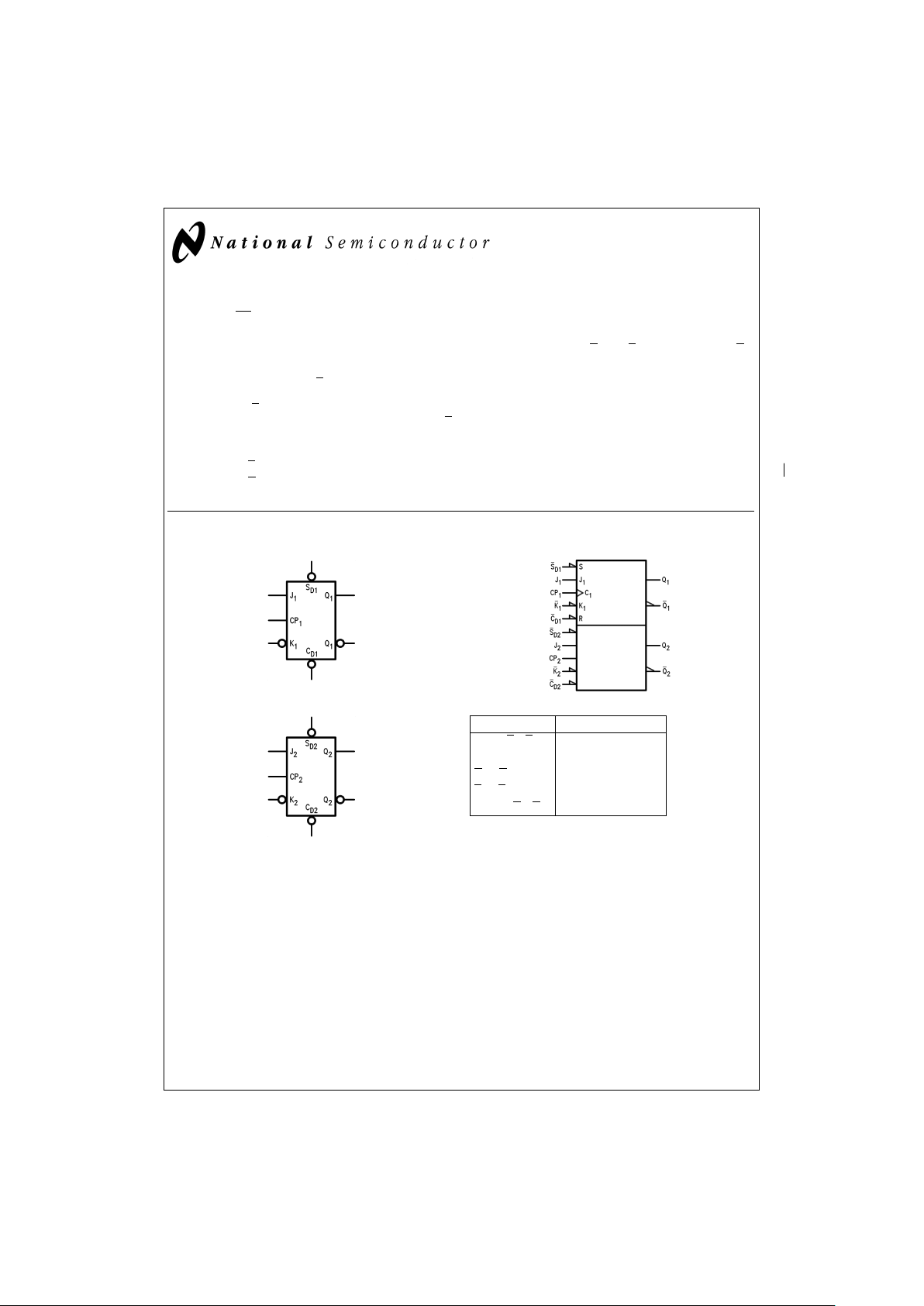
54AC109•54ACT109
Dual JK Positive Edge-Triggered Flip-Flop
General Description
The ’AC/’ACT109 consists of two high-speed completely independent transition clocked JK flip-flops. The clocking operation is independent of rise and fall times of the clock
waveform. The JK design allows operation as a D flip-flop
(refer to ’AC/’ACT74 data sheet) by connecting the J and K
inputs together.
Asynchronous Inputs:
LOW input to S
D
(Set) sets Q to HIGH level
LOW input to CD(Clear) sets Q to LOW level
Clear and Set are independent of clock
Simultaneous LOW on C
D
and SDmakes both Q and Q
HIGH
Features
n ICCreduced by 50
%
n Outputs source/sink 24 mA
n ’ACT109 has TTL-compatible inputs
n Standard Military Drawing (SMD)
—’AC109: 5962-89551
—’ACT109: 5962-88534
Logic Symbol
Pin Names Description
J
1,J2,K1,K2
Data Inputs
CP
1
,CP
2
Clock Pulse Inputs
C
D1,CD2
Direct Clear Inputs
S
D1,SD2
Direct Set Inputs
Q
1,Q2,Q1,Q2
Outputs
FACT®is a registered trademark of Fairchild Semiconductor Corporation.
DS100267-1
DS100267-2
IEEE/IEC
DS100267-7
August 1998
54AC109
•
54ACT109 Dual JK Positive Edge-Triggered Flip-Flop
© 1998 National Semiconductor Corporation DS100267 www.national.com
Page 2
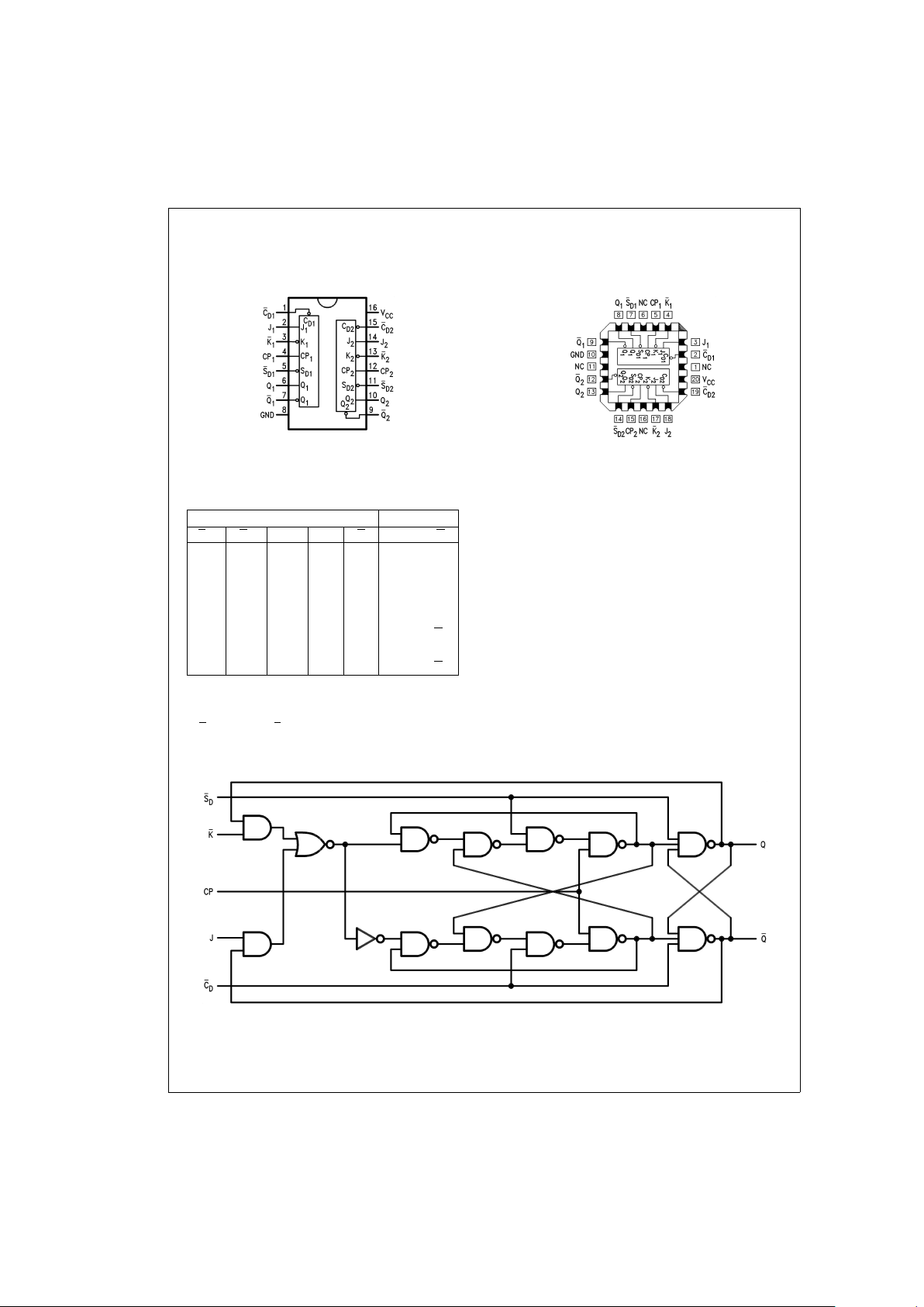
Connection Diagrams
Truth Table
(each half)
Inputs Outputs
S
D
C
D
CP J K QQ
LHXXXHL
HLXXXLH
LLXXXHH
HH
N
LL L H
HH
N
H L Toggle
HH
N
LHQ0Q
0
HH
N
HH H L
HHLXXQ
0
Q
0
H
=
HIGH Voltage Level
L=LOW Voltage Level
N
=
LOW-to-HIGH Transition
X=Immaterial
Q
0(Q0
)=Previous Q0(Q0) before LOW-to-HIGH Transition of Clock
Logic Diagram (one half shown)
Pin Assignment
for DIP and Flatpak
DS100267-3
Pin Assignment
for LCC
DS100267-4
DS100267-5
Please note that this diagram is provided only for the understanding of logic operations and should not be used to estimate propagation delays.
www.national.com 2
Page 3
Absolute Maximum Ratings (Note 1)
If Military/Aerospace specified devices are required,
please contact the National Semiconductor Sales Office/
Distributors for availability and specifications.
Supply Voltage (V
CC
) −0.5V to +7.0V
DC Input Diode Current (I
IK
)
V
I
=
−0.5V −20 mA
V
I
=
V
CC
+ 0.5V +20 mA
DC Input Voltage (V
I
) −0.5V to VCC+ 0.5V
DC Output Diode Current (I
OK
)
V
O
=
−0.5V −20 mA
V
O
=
V
CC
+ 0.5V +20 mA
DC Output Voltage (V
O
) −0.5V to VCC+ 0.5V
DC Output Source
or Sink Current (I
O
)
±
50 mA
DC V
CC
or Ground Current
per Output Pin (I
CC
or I
GND
)
±
50 mA
Storage Temperature (T
STG
) −65˚C to +150˚C
Junction Temperature (T
J
)
CDIP 175˚C
Recommended Operating
Conditions
Supply Voltage (VCC)
’AC 2.0V to 6.0V
’ACT 4.5V to 5.5V
Input Voltage (V
I
) 0VtoV
CC
Output Voltage (VO) 0VtoV
CC
Operating Temperature (TA)
54AC/ACT −55˚C to +125˚C
Minimum Input Edge Rate (∆V/∆t)
’AC Devices
V
IN
from 30%to 70%of V
CC
V
CC
@
3.3V, 4.5V, 5.5V 125 mV/ns
Minimum Input Edge Rate (∆V/∆t)
’ACT Devices
V
IN
from 0.8V to 2.0V
V
CC
@
4.5V, 5.5V 125 mV/ns
Note 1: Absolute maximum ratings are those values beyond which damage
to the device may occur. The databook specifications should be met, without
exception, to ensure that the system design is reliable over its power supply,
temperature, and output/input loading variables. National does not recommend operation of FACT
®
circuits outside databook specifications.
DC Characteristics for ’AC Family Devices
54AC
Symbol Parameter V
CC
T
A
=
−55˚C to +125˚C Units Conditions
(V) Guaranteed Limits
V
IH
Minimum High Level 3.0 2.1 V
OUT
=
0.1V
Input Voltage 4.5 3.15 V or V
CC
− 0.1V
5.5 3.85
V
IL
Maximum Low Level 3.0 0.9 V
OUT
=
0.1V
Input Voltage 4.5 1.35 V or V
CC
− 0.1V
5.5 1.65
V
OH
Minimum High Level 3.0 2.9 I
OUT
=
−50 µA
Output Voltage 4.5 4.4 V
5.5 5.4
(Note 2)
V
IN
=
V
IL
or V
IH
3.0 2.4 I
OH
=
−12 mA
4.5 3.7 V I
OH
=
−24 mA
5.5 4.7 I
OH
=
−24 mA
V
OL
Maximum Low Level 3.0 0.1 I
OUT
=
50 µA
Output Voltage 4.5 0.1 V
5.5 0.1
(Note 2)
V
IN
=
V
IL
or V
IH
3.0 0.5 I
OL
=
12 mA
4.5 0.5 V I
OL
=
24 mA
5.5 0.5 I
OL
=
24 mA
I
IN
Maximum Input 5.5
±
1.0 µA V
I
=
V
CC
, GND
Leakage Current
(Note 3)
Minimum Dynamic
Output Current
I
OLD
5.5 50 mA V
OLD
=
1.65V Max
I
OHD
5.5 −50 mA V
OHD
=
3.85V Min
3 www.national.com
Page 4

DC Characteristics for ’AC Family Devices (Continued)
54AC
Symbol Parameter V
CC
T
A
=
−55˚C to +125˚C Units Conditions
(V) Guaranteed Limits
I
CC
Maximum Quiescent 5.5 40.0 µA V
IN
=
V
CC
Supply Current or GND
Note 2: All outputs loaded; thresholds on input associated with output under test.
Note 3: Maximum test duration 2.0 ms, one output loaded at a time.
Note 4: I
IN
and I
CC
@
3.0V are guaranteed to be less than or equal to the respective limit@5.5V VCC.
I
CC
for 54AC@25˚C is identical to 74AC@25˚C.
DC Characteristics for ’ACT Family Devices
54ACT
Symbol Parameter V
CC
T
A
=
−55˚C to +125˚C Units Conditions
(V) Guaranteed Limits
V
IH
Minimum High Level 4.5 2.0 V V
OUT
=
0.1V
Input Voltage 5.5 2.0 or V
CC
− 0.1V
V
IL
Maximum Low Level 4.5 0.8 V V
OUT
=
0.1V
Input Voltage 5.5 0.8 or V
CC
− 0.1V
V
OH
Minimum High Level 4.5 4.4 V I
OUT
=
−50 µA
Output Voltage 5.5 5.4
(Note 5)
V
IN
=
V
IL
or V
IH
4.5 3.70 V I
OH
=
−24 mA
5.5 4.70 I
OH
=
−24 mA
V
OL
Maximum Low Level 4.5 0.1 V I
OUT
=
50 µA
Output Voltage 5.5 0.1
(Note 5)
V
IN
=
V
IL
or V
IH
4.5 0.50 V I
OL
=
24 mA
5.5 0.50 I
OL
=
24 mA
I
IN
Maximum Input 5.5
±
1.0 µA V
I
=
V
CC
, GND
Leakage Current
I
CCT
Maximum 5.5 1.6 mA V
I
=
V
CC
− 2.1V
I
CC
/Input
(Note 6)
I
OLD
Minimum Dynamic 5.5 50 mA V
OLD
=
1.65V Max
I
OHD
Output Current 5.5 −50 mA V
OHD
=
3.85V Min
I
CC
Maximum Quiescent 5.5 40.0 µA V
IN
=
V
CC
Supply Current or GND
Note 5: All outputs loaded; thresholds on input associated with output under test.
Note 6: Maximum test duration 2.0 ms, one output loaded at a time.
Note 7: I
CC
for 54ACT@25˚C is identical to 74ACT@25˚C.
www.national.com 4
Page 5

AC Electrical Characteristics
54AC
V
CC
T
A
=
−55˚C Fig.
Symbol Parameter (V) to +125˚C Units No.
(Note 8) C
L
=
50 pF
Min Max
f
max
Maximum Clock 3.3 65 MHz
Frequency 5.0 95
t
PLH
Propagation Delay 3.3 1.0 17.5 ns
CP
n
to Qnor Q
n
5.0 1.0 12.0
t
PHL
Propagation Delay 3.3 1.0 13.5 ns
CP
n
to Qnor Q
n
5.0 1.0 10.0
t
PLH
Propagation Delay 3.3 1.0 13.0 ns
C
Dn
or SDnto Qnor Q
n
5.0 1.0 9.5
t
PHL
Propagation Delay 3.3 1.0 14.0 ns
C
Dn
or SDnto Qnor Q
n
5.0 1.0 10.5
Note 8: Voltage Range 3.3 is 3.3V±0.3V
Voltage Range 5.0 is 5.0V
±
0.5V
AC Operating Requirements
54AC
V
CC
T
A
=
−55˚C Fig.
Symbol Parameter (V) to +125˚C Units No.
(Note 9) C
L
=
50 pF
Guaranteed
Minimum
t
s
Setup Time, HIGH or LOW 3.3 8.0 ns
J
n
or Knto CP
n
5.0 5.5
t
h
Hold Time, HIGH or LOW 3.3 0 ns
J
n
or Knto CP
n
5.0 0.5
t
w
Pulse Width 3.3 8.0 ns
C
Dn
or SDnor CP
n
5.0 5.5
t
rec
Recovery Time 3.3 0.5 ns
C
Dn
or SDnto CP
n
5.0 0.5
Note 9: Voltage Range 3.3 is 3.3V±0.3V
Voltage Range 5.0 is 5.0V
±
0.5V
5 www.national.com
Page 6

AC Electrical Characteristics
54ACT
V
CC
T
A
=
−55˚C
Symbol Parameter (V) to +125˚C Units
(Note 10) C
L
=
50 pF
Min Max
f
max
Maximum Clock 5.0 85 MHz
Frequency
t
PLH
Propagation Delay 5.0 1.0 14.0 ns
CP
n
to Qnor Q
n
t
PHL
Propagation Delay 5.0 1.0 12.0 ns
CP
n
to Qnor Q
n
t
PLH
Propagation Delay 5.0 1.0 11.5 ns
C
Dn
or SDnto Qnor Q
n
t
PHL
Propagation Delay 5.0 1.0 12.5 ns
C
Dn
or SDnto Qnor Q
n
Note 10: Voltage Range 5.0 is 5.0V±0.5V
AC Operating Requirements
54ACT
V
CC
T
A
=
−55˚C
Symbol Parameter (V) to +125˚C Units
(Note 11) C
L
=
50 pF
Guaranteed
Minimum
t
s
Setup Time, HIGH or LOW 5.0 2.5 ns
J
n
or Knto CP
n
t
h
Hold Time, HIGH or LOW 5.0 2.0 ns
J
n
or Knto CP
n
t
w
Pulse Width 5.0 5.0 ns
CP
n
or CDnor S
Dn
t
rec
Recovery Time 5.0 0.5 ns
C
Dn
or SDnto CP
n
Note 11: Voltage Range 5.0 is 5.0V±0.5V
Capacitance
Symbol Parameter Typ Units Conditions
C
IN
Input Capacitance 4.5 pF V
CC
=
OPEN
C
PD
Power Dissipation 35.0 pF V
CC
=
5.0V
Capacitance
www.national.com 6
Page 7

Physical Dimensions inches (millimeters) unless otherwise noted
20 Terminal Ceramic Leadless Chip Carrier (L)
NS Package Number E20A
16 Lead Ceramic Dual-In-Line Package (D)
NS Package Number J16A
7 www.national.com
Page 8

Physical Dimensions inches (millimeters) unless otherwise noted (Continued)
LIFE SUPPORT POLICY
NATIONAL’S PRODUCTS ARE NOT AUTHORIZED FOR USE AS CRITICAL COMPONENTS IN LIFE SUPPORT DEVICES OR SYSTEMS WITHOUT THE EXPRESS WRITTEN APPROVAL OF THE PRESIDENT OF NATIONAL SEMICONDUCTOR CORPORATION. As used herein:
1. Life support devices or systems are devices or systems which, (a) are intended for surgical implant into
the body, or (b) support or sustain life, and whose failure to perform when properly used in accordance
with instructions for use provided in the labeling, can
be reasonably expected to result in a significant injury
to the user.
2. A critical component in any component of a life support
device or system whose failure to perform can be reasonably expected to cause the failure of the life support
device or system, or to affect its safety or effectiveness.
National Semiconductor
Corporation
Americas
Tel: 1-800-272-9959
Fax: 1-800-737-7018
Email: support@nsc.com
www.national.com
National Semiconductor
Europe
Fax: +49 (0) 1 80-530 85 86
Email: europe.support@nsc.com
Deutsch Tel: +49 (0) 1 80-530 85 85
English Tel: +49 (0) 1 80-532 78 32
Français Tel: +49 (0) 1 80-532 93 58
Italiano Tel: +49 (0) 1 80-534 16 80
National Semiconductor
Asia Pacific Customer
Response Group
Tel: 65-2544466
Fax: 65-2504466
Email: sea.support@nsc.com
National Semiconductor
Japan Ltd.
Tel: 81-3-5620-6175
Fax: 81-3-5620-6179
16 Lead Ceramic Flatpak (F)
NS Package Number W16A
54AC109
•
54ACT109 Dual JK Positive Edge-Triggered Flip-Flop
National does not assume any responsibility for use of any circuitry described, no circuit patent licenses are implied and National reserves the right at any time without notice to change said circuitry and specifications.
 Loading...