

Page 1
4N47
4N48
JAN, JANTX, JANTXV, SINGLE CHANNEL OPTOCOUPLERS
4N49
Features:
• High Reliability
• Base lead provided for conventional transistor
biasing
• Rugged package
• High gain, high voltage transistor
• +1kV electrical isolation
DESCRIPTION
Gallium Aluminum Arsenide (GaAlAs) infrared LED and a high gain N-P-N silicon phototransistor packaged in a hermetically
sealed TO-5 metal can. The 4N47, 4N48 and 4N49’s can be tested to customer specifications, as well as to MIL-PRF-19500
JAN, JANTX, JANTXV and JANS quality levels.
*ABSOLUTE MAXIMUM RATINGS
Input to Output Voltage.............................................................................................................................................................1kV
Emitter-Collector Voltage............................................................................................................................................................7V
Collector-Emitter Voltage (Value applies to emitter-base open-circuited & the input-diode equal to zero) ............................40V
Collector-Base Voltage .............................................................................................................................................................45V
Reverse Input Voltage ...............................................................................................................................................................2V
Input Diode Continuous Forward Current at (or below) 65°C Free-Air Temperature (see note 1) ......................................40mA
Peak Forward Input Current (Value applies for tw
< 1µs, PRR < 300 pps) ...............................................................................1A
Continuous Collector Current ................................................................................................................................................50mA
Continuous Transistor Power Dissipation at (or below) 25°C Free-Air Temperature (see Note 2) ..................................300mW
Storage Temperature........................................................................................................................................... -65°C to +125°C
Operating Free-Air Temperature Range ............................................................................................................. -55°C to +125°C
Lead Solder Temperature (1/16” (1.6mm) from case for 10 seconds) ................................................................................ 240°C
Notes:
1. Derate linearly to 125°C free-air temperature at the rate of 0.67 mA/°C above 65°C.
2. Derate linearly to 125°C free-air temperature at the rate of 3 mW/°C.
*JEDEC registered data
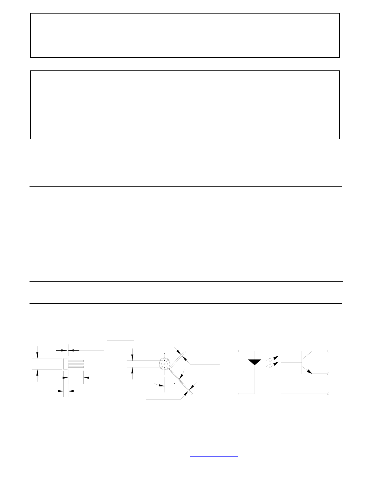
Package Dimensions Schematic Diagram
Applications:
• Eliminate ground loops
• Level shifting
• Line receiver
• Switching power supplies
• Motor control
Mii
OPTOELECTRONIC
PRODUCTS{PRIVATE }
DIVISION
6 LEADS
0.016Ø [0.41]
0.040 [1.02]
MAX.
0.305 [7.75]
0.335 [8.51]
0.155 [3.94]
0.185 [4.70]
NOTE: ALL LINEAR DIMENSI ONS ARE IN INCHES (MILLIMETERS)
0.019Ø[0.48]
0.500 [12.70]
MIN.
0.022Ø [5.08]
5
6
3
2
1
0.034 [0.864]
0.028 [0.711]
A
5
7
45°
0.045 [1.14]
0.029 [0.73]
K
7
MICROPAC INDUSTRIES, INC. OPTOELECTRONIC PRODUCTS DIVISION • 725 E.Walnut St., Garland, TX 75040 • (972) 272-3571 • Fax (972) 487-6918
www.micropac.com E-MAIL: optosales@micropac.com
3 - 14
C
3
E
1
B
2
Page 2
4N47, 4N48, and 4N49 JAN, JANTX, JANTXV, JANS, SINGLE CHANNEL OPTOCOUPLERS
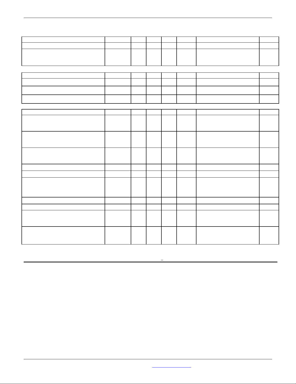
*ELECTRICAL CHARACTERISTICS T
= 25°C Unless otherwise specified
A
PARAMETER SYMBOL MIN TYP MAX UNITS TEST CONDITIONS NOTE
Input Diode Static Reverse Current I
Input Diode Static Forward Voltage -55°C
+25°C
+100
*OUTPUT TRANSISTOR T
A
°
C
= 25°C Unless otherwise specified
R
V
F
100 µA VR = 2V
1.0
0.8
0.7
1.4
1.7
1.5
1.3
V
IE = 10mA
PARAMETER SYMBOL MIN TYP MAX UNITS TEST CONDITIONS NOTE
Collector-Base Breakdown Voltage V
Collector-Emitter Breakdown Voltage V
Emitter-Collector Breakdown Voltage V
*COUPLED CHARACTERISTICS T
= 25°C Unless otherwise specified
A
45 V IC = 100µA, I
(BR)CBO
40 V IC = 1mA, I
(BR)CEO
(BR)EBO
7
V IC = 0, IE = 100µA, IF = 0
= 0, IF = 0
B
= 0, IF = 0
B
PARAMETER SYMBOL MIN TYP MAX UNITS TEST CONDITIONS NOTE
On State Collector Current 4N47
4N48
4N49
On State Collector Current 4N47
-55°C 4N48
4N49
On State Collector Current 4N47
+100°C 4N48
4N49
Off State Collector Current +25°C I
Off State Collector Current +100°C I
Collector-Emitter Saturation Voltage 4N47
4N48
4N49
Input to Output Resistance R
Input to Output Capacitance C
Rise Time/ Fall Time 4N47
Phototransistor Operation 4N48
4N49
Rise Time/ Fall Time 4N47
Photodiode Operation 4N48
4N49
NOTES:
1. These parameters are measured between all phototransistor leads shorted together and with both input diode leads shorted together.
2. This parameter measured using pulse techniques t
I
C(ON)
I
C(ON)
0.5
1.0
2.0
0.7
1.4
mA
5
10
mA
2.8
I
C(ON)
0.5
1.0
mA
2.0
C(OFF)
C(OFF)
V
CE(SAT)
V
CE(SAT)
V
CE(SAT)
10
I-O
5 pF f = 1MHz, V
I-O
t
/ t
r
f
t
/ t
r
f
t
/ t
r
f
tr / t
f
tr / t
f
tr / t
f
w
100 nA VCE = 20V, I
100 µA VCE = 20V, I
0.3
11
V
20
0.85
0.3
0.3
25
25
0.85
0.85
V
V
V
µs
µs
µs
µs
µs
µs
=100µs, duty cycle < 1%.
VCC = 10V, IF = 10mA, RL = 100Ω
VCC = 10V, IF = 10mA, RL = 100Ω
VCE = 5V, I
VCE = 5V, I
VCE = 5V, I
IC = 0.5mA, I
IC = 1mA, I
IC = 2mA, I
IN-OUT
= 0, IF = 1mA
B
= 0, IF = 2mA
B
= 0, IF = 2mA
B
= 0, IF = 0mA
B
= 0, IF = 0mA
B
= 0, IF = 2mA
B
= 0, IF = 2mA
B
= 0, IF = 2mA
B
= 1kV 1
= 1kV 1
IN-OUT
MICROPAC INDUSTRIES, INC. OPTOELECTRONIC PRODUCTS DIVISION • 725 E.Walnut St., Garland, TX 75040 • (972) 272-3571 • Fax (972) 487-6918
www.micropac.com E-MAIL: optosales@micropac.com
3 - 15
2
Page 3

4N47, 4N48, and 4N49 JAN, JANTX, JANTXV, JANS, SINGLE CHANNEL OPTOCOUPLERS
RECOMMENDED OPERATING CONDITIONS:
PARAMETER SYMBOL MIN MAX UNITS
Input Current, Low Level I
Input Current, High Level I
Supply Voltage V
FL
FH
CE
0 100 µA
2 10 mA
5 10 V
SELECTION GUIDE
PART NUMBER PART DESCRIPTION
JAN4N47 4N47 Optocoupler, JAN Screening level
JAN4N48 4N48 Optocoupler, JAN Screening level
JAN4N49 4N49 Optocoupler, JAN Screening level
JANTX4N47 4N47 Optocoupler, JANTX Screening level
JANTX4N48 4N48 Optocoupler, JANTX Screening level
JANTX4N49 4N49 Optocoupler, JANTX Screening level
JANTXV4N47 4N47 Optocoupler, JANTXV Screening level
JANTXV4N48 4N48 Optocoupler, JANTXV Screening level
JANTXV4N49 4N49 Optocoupler, JANTXV Screening level
JANS4N47 4N47 Optocoupler, JANS Screening level
JANS4N48 4N48 Optocoupler, JANS Screening level
*JEDEC registered data
JANS4N49 4N49 Optocoupler, JANS Screening level
MICROPAC INDUSTRIES, INC. OPTOELECTRONIC PRODUCTS DIVISION • 725 E.Walnut St., Garland, TX 75040 • (972) 272-3571 • Fax (972) 487-6918
www.micropac.com E-MAIL: optosales@micropac.com
3 - 16
 Loading...