

Page 1
MOTOROLA
SEMICONDUCTOR TECHNICAL DATA
Order this document
by J308/D
JFET VHF/UHF Amplifiers
N–Channel — Depletion
GATE
MAXIMUM RATINGS
Rating Symbol Value Unit
Drain–Source Voltage V
Gate–Source Voltage V
Forward Gate Current I
Total Device Dissipation @ TA = 25°C
Derate above 25°C
Junction Temperature Range T
Storage Temperature Range T
ELECTRICAL CHARACTERISTICS (T
Characteristic
DS
GS
GF
P
D
J
stg
= 25°C unless otherwise noted)
A
OFF CHARACTERISTICS
Gate–Source Breakdown Voltage
(IG = –1.0 µAdc, VDS = 0)
Gate Reverse Current
(VGS = –15 Vdc, VDS = 0, TA = 25°C)
(VGS = –15 Vdc, VDS = 0, TA = +125°C)
Gate Source Cutoff Voltage
(VDS = 10 Vdc, ID = 1.0 nAdc) J308
ON CHARACTERISTICS
Zero–Gate–Voltage Drain Current
(VDS = 10 Vdc, VGS = 0) J308
Gate–Source Forward Voltage
(VDS = 0, IG = 1.0 mAdc)
(1)
SMALL–SIGNAL CHARACTERISTICS
Common–Source Input Conductance
(VDS = 10 Vdc, ID = 10 mAdc, f = 100 MHz) J308
Common–Source Output Conductance
(VDS = 10 Vdc, ID = 10 mAdc, f = 100 MHz)
Common–Gate Power Gain
(VDS = 10 Vdc, ID = 10 mAdc, f = 100 MHz)
1. Pulse Test: Pulse Width v 300 µs, Duty Cycle v 3.0%.
25 Vdc
25 Vdc
10 mAdc
350
2.8
–65 to +125 °C
–65 to +150 °C
J309
J310
J309
J310
J309
J310
J308
1 DRAIN
J309
J310
3
2 SOURCE
mW
mW/°C
Symbol Min Typ Max Unit
V
(BR)GSS
I
GSS
V
GS(off)
I
DSS
V
GS(f)
Re(yis)
Re(yos) — 0.25 — mmhos
G
pg
–25 — — Vdc
—
—
–1.0
–1.0
–2.0
12
12
24
— — 1.0 Vdc
—
—
—
— 16 — dB
Motorola Preferred Devices
1
2
3
CASE 29–04, STYLE 5
TO–92 (TO–226AA)
—
—
—
—
—
—
—
—
0.7
0.7
0.5
–1.0
–1.0
–6.5
–4.0
–6.5
60
30
60
—
—
—
nAdc
µAdc
Vdc
mAdc
mmhos
Motorola Small–Signal Transistors, FETs and Diodes Device Data
Motorola, Inc. 1997
1
Page 2
J308 J309 J310
ELECTRICAL CHARACTERISTICS
Characteristic
(TA = 25°C unless otherwise noted) (Continued)
SMALL–SIGNAL CHARACTERISTICS (continued)
Common–Source Forward Transconductance
(VDS = 10 Vdc, ID = 10 mAdc, f = 100 MHz)
Common–Gate Input Conductance
(VDS = 10 Vdc, ID = 10 mAdc, f = 100 MHz)
Common–Source Forward Transconductance
(VDS = 10 Vdc, ID = 10 mAdc, f = 1.0 kHz) J308
Common–Source Output Conductance
(VDS = 10 Vdc, ID = 10 mAdc, f = 1.0 kHz)
Common–Gate Forward Transconductance
(VDS = 10 Vdc, ID = 10 mAdc, f = 1.0 kHz) J308
Common–Gate Output Conductance
(VDS = 10 Vdc, ID = 10 mAdc, f = 1.0 kHz) J308
Gate–Drain Capacitance
(VDS = 0, VGS = –10 Vdc, f = 1.0 MHz)
Gate–Source Capacitance
(VDS = 0, VGS = –10 Vdc, f = 1.0 MHz)
FUNCTIONAL CHARACTERISTICS
Noise Figure
(VDS = 10 Vdc, ID = 10 mAdc, f = 450 MHz)
Equivalent Short–Circuit Input Noise Voltage
(VDS = 10 Vdc, ID = 10 mAdc, f = 100 Hz)
J309
J310
J309
J310
J309
J310
Symbol Min Typ Max Unit
Re(yfs) — 12 — mmhos
Re(yig) — 12 — mmhos
g
fs
g
os
g
fg
g
og
C
gd
C
gs
NF — 1.5 — dB
e
n
8000
10000
8000
— — 250 µmhos
—
—
—
—
—
—
— 1.8 2.5 pF
— 4.3 5.0 pF
— 10 —
—
—
—
13000
13000
12000
150
100
150
20000
20000
18000
—
—
—
—
—
—
µmhos
µmhos
µmhos
nVńHz
Ǹ
2
Motorola Small–Signal Transistors, FETs and Diodes Device Data
Page 3
J308 J309 J310
50
50
310
F
W
T
T
Y
Ω
SOURCE
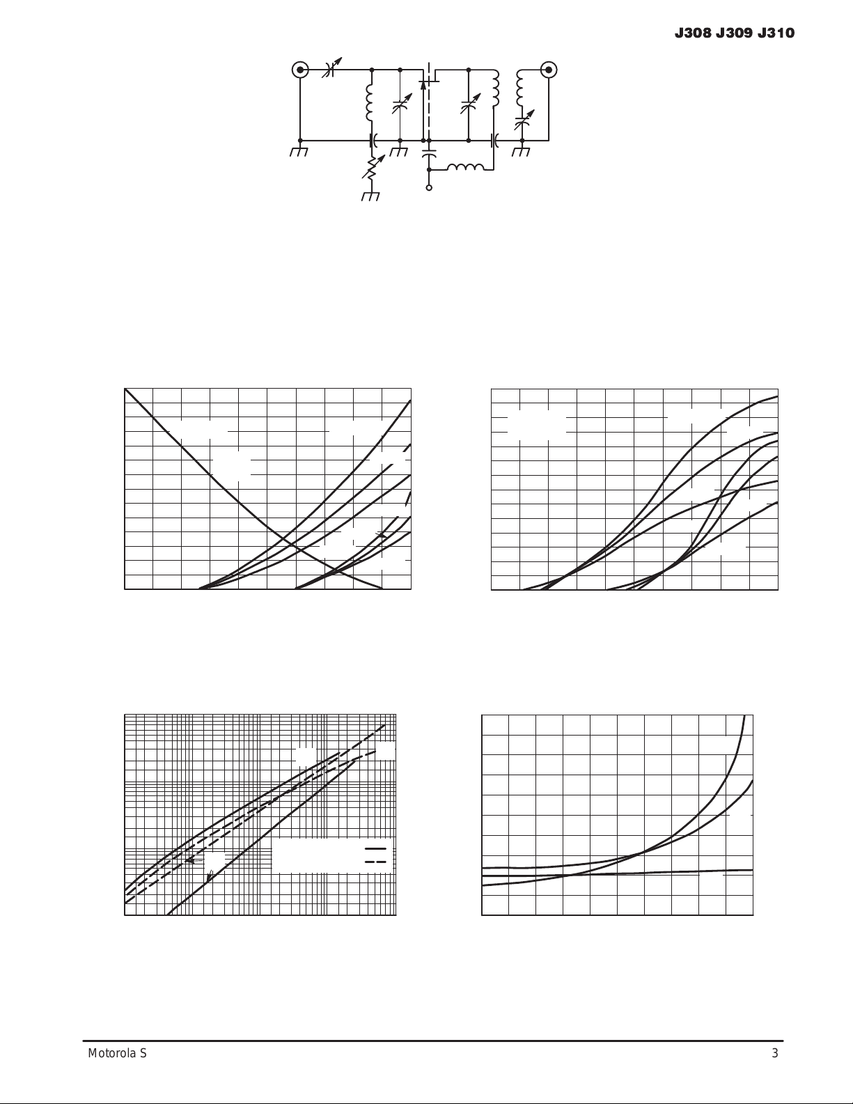
Figure 1. 450 MHz Common–Gate Amplifier Test Circuit
70
60
50
40
30
, DRAIN CURRENT (mA)I
20
D
10
–5.0 –4.0 –3.0 –2.0
VDS = 10 V
I
DSS
+25°C
ID – VGS, GATE–SOURCE VOLTAGE (VOLTS)
I
– VGS, GATE–SOURCE CUTOFF VOLTAGE (VOLTS)
DSS
Figure 2. Drain Current and Transfer
Characteristics versus Gate–Source V oltage
U
C3
L1
C1
C5
1.0 k
+V
DD
C1 = C2 = 0.8 – 10 pF, JFD #MVM010W.
C3 = C4 = 8.35 pF Erie #539–002D.
C5 = C6 = 5000 pF Erie (2443–000).
C7 = 1000 pF, Allen Bradley #FA5C.
RFC = 0.33 µH Miller #9230–30.
L1 = One Turn #16 Cu, 1/4″ I.D. (Air Core).
L2P = One Turn #16 Cu, 1/4″ I.D. (Air Core).
L2S = One Turn #16 Cu, 1/4″ I.D. (Air Core).
70
+25°C
+150°C
+150°C
60
50
40
30
20
10
0
TA = –55°C
+25°C
–55°C
–1.0 0
C7
, SATURATION DRAIN CURRENT (mA)
DSS
I
L2
P
C2
C6
RFC
35
30
VDS = 10 V
f = 1.0 MHz
25
20
15
10
5.0
, FORWARD TRANSCONDUCTANCE (mmhos)Y
fs
0
5.0 4.0 3.0 2.0
Ω
LOAD
L2
S
C4
TA = –55°C
+25°C
+150°C
–55°C
+150°C
1.0 0
VGS, GATE–SOURCE VOLTAGE (VOLTS)
Figure 3. Forward Transconductance
versus Gate–Source V oltage
+25°C
100 k
µ
Y
V
GS(off)
V
GS(off)
fs
= –2.3 V =
= –5.7 V =
ANCE ( mhos)
10 k
RANSCONDUC
1.0 k
ARD
OR
,
fs
100
0.01 0.10.2 0.3 0.5 1.0 2.03.0 5.0 10 20 30 50 100
Figure 4. Common–Source Output
Admittance and Forward Transconductance
Y
os
ID, DRAIN CURRENT (mA)
versus Drain Current
1.0 k
Y
fs
µ
100
10
, OUTPUT ADMITTANCE ( mhos)Y
1.0
Motorola Small–Signal Transistors, FETs and Diodes Device Data
os
10
7.0
4.0
CAPACITANCE (pF)
1.0
0
5.0 4.0 3.0 2.0 1.0 06.07.08.09.010
VGS, GATE SOURCE VOLTAGE (VOLTS)
Figure 5. On Resistance and Junction
Capacitance versus Gate–Source V oltage
120
R
DS
96
72
C
gs
48
, ON RESISTANCE (OHMS)R
DS
C
gd
24
0
3
Page 4

J308 J309 J310
30
VDS = 10 V
24
ID = 10 mA
| (mmhos)
18
22
|, |Y
21
12
|, |Y
11
|Y
6.0
0
TA = 25°C
f, FREQUENCY (MHz)
Y
Y
Y
Figure 6. Common–Gate Y Parameter
Magnitude versus Frequency
θ21, θ
11
50°
180°
θ
22
40°
170°
160°
150°
140°
130°
30°
20°
10°
θ
12
0°
f, FREQUENCY (MHz)
θ
11
θ
21
VDS = 10 V
ID = 10 mA
TA = 25°C
|S21|, |S11|
0.45
3.0
2.4
11
21
22
Y
12
1.8
(mmhos)
12
1.2
Y
0.6
1000100 200 300 500 700
0.85
0.79
0.73
0.67
0.61
0.55
0.39
0.33
0.27
0.21
0.15
VDS = 10 V
ID = 10 mA
TA = 25°C
f, FREQUENCY (MHz)
S
22
S
21
S
11
S
12
|S12|, |S22|
0.060
0.048
0.036
0.024
0.012
1000100 200 300 500 700
1.00
0.98
0.96
0.94
0.92
0.90
Figure 7. Common–Gate S Parameter
Magnitude versus Frequency
1000100 200 300 500 700
θ12, θ
–20°
–20°
–40°
–60°
–80°
–100°
–120°
–140°
–160°
–180°
–200°
22
87°
86°
85°
84°
83°
82°
θ11, θ
–20°
–40°
–60°
–80°
–100°
–120°
12
120°
100°
80°
60°
40°
20°
θ
11
θ
21
θ
12
VDS = 10 V
ID = 10 mA
TA = 25°C
f, FREQUENCY (MHz)
θ
22
θ
θ21, θ
22
0
–20°
–40°
–60°
θ
21
–80°
11
–100°
1000100 200 300 500 700
Figure 8. Common–Gate Y Parameter
Phase–Angle versus Frequency
8.0
VDD = 20 V
7.0
f = 450 MHz
BW ≈ 10 MHz
6.0
CIRCUIT IN FIGURE 1
5.0
4.0
3.0
NF , NOISE FIGURE (dB)
2.0
1.0
0
4.0 6.0 8.0 10 12 14 16 18 20 22 24
G
pg
NF
Figure 10. Noise Figure and
Power Gain versus Drain Current
4
Figure 9. S Parameter Phase–Angle
versus Frequency
24
21
18
15
12
9.0
pg
G , POWER GAIN (dB)
6.0
3.0
0
7.0
6.0
5.0
4.0
VDS = 10 V
ID = 10 mA
TA = 25°C
3.0
CIRCUIT IN FIGURE 1
2.0
NF , NOISE FIGURE (dB)
1.0
0
G
pg
NF
50 100 200 300 500 700 1000
f, FREQUENCY (MHz)ID, DRAIN CURRENT (mA)
Figure 11. Noise Figure and Power Gain
versus Frequency
Motorola Small–Signal Transistors, FETs and Diodes Device Data
26
22
18
14
10
pg
G , POWER GAIN (dB)
6.0
2.0
Page 5

J308 J309 J310
INPUT
RS = 50 Ω
C1
C2
U310
S
L1
L2
V
S
C3
G
SHIELD
D
C4
C6
BW (3 dB) – 36.5 MHz
ID – 10 mAdc
L3
OUTPUT
RL = 50 Ω
C5
L4
V
D
VDS – 20 Vdc
Device case grounded
IM test tones – f1 = 449.5 MHz, f2 = 450.5 MHz
C1 = 1–10 pF Johanson Air variable trimmer.
C2, C5 = 100 pF feed thru button capacitor.
C3, C4, C6 = 0.5–6 pF Johanson Air variable
trimmer.
L1 = 1/8″ x 1/32″ x 1–5/8″ copper bar.
L2, L4 = Ferroxcube Vk200 choke.
L3 = 1/8″ x 1/32″ x 1–7/8″ copper bar.
Figure 12. 450 MHz IMD Evaluation Amplifier
Amplifier power gain and IMD products are a function of the load impedance. For the amplifier design shown above with C4 and
C6 adjusted to reflect a load to the drain resulting in a nominal power gain of 9 dB, the 3rd order intercept point (IP) value is
29 dBm. Adjusting C4, C6 to provide larger load values will result in higher gain, smaller bandwidth and lower IP values. For
example, a nominal gain of 13 dB can be achieved with an intercept point of 19 dBm.
+40
+20
–20
–40
–60
–80
OUTPUT POWER PER TONE (dBm)
–100
–120
U310 JFET
VDS = 20 Vdc
ID = 10 mAdc
0
F1 = 449.5 MHz
F2 = 450.5 MHz
–120
FUNDAMENTAL OUTPUT
–100 –80
INPUT POWER PER TONE (dBm)
3RD ORDER INTERCEPT POINT
3RD ORDER IMD OUTPUT
–60
–40 –20 0
Example of intercept point plot use:
Assume two in–band signals of –20 dBm at the amplifier input.
They will result in a 3rd order IMD signal at the output of
–90 dBm. Also, each signal level at the output will be
–11 dBm, showing an amplifier gain of 9.0 dB and an
intermodulation ratio (IMR) capability of 79 dB. The gain and
IMR values apply only for signal levels below comparison.
+20
Figure 13. Two Tone 3rd Order Intercept Point
Motorola Small–Signal Transistors, FETs and Diodes Device Data
5
Page 6

J308 J309 J310
R
SEATING
PLANE
XX
P ACKAGE DIMENSIONS
NOTES:
1. DIMENSIONING AND TOLERANCING PER ANSI
A
B
P
L
F
K
D
G
H
V
1
C
SECTION X–X
N
J
N
Y14.5M, 1982.
2. CONTROLLING DIMENSION: INCH.
3. CONTOUR OF PACKAGE BEYOND DIMENSION R
IS UNCONTROLLED.
4. DIMENSION F APPLIES BETWEEN P AND L.
DIMENSION D AND J APPLY BETWEEN L AND K
MINIMUM. LEAD DIMENSION IS UNCONTROLLED
IN P AND BEYOND DIMENSION K MINIMUM.
DIM MIN MAX MIN MAX
A 0.175 0.205 4.45 5.20
B 0.170 0.210 4.32 5.33
C 0.125 0.165 3.18 4.19
D 0.016 0.022 0.41 0.55
F 0.016 0.019 0.41 0.48
G 0.045 0.055 1.15 1.39
H 0.095 0.105 2.42 2.66
J 0.015 0.020 0.39 0.50
K 0.500 ––– 12.70 –––
L 0.250 ––– 6.35 –––
N 0.080 0.105 2.04 2.66
P ––– 0.100 ––– 2.54
R 0.115 ––– 2.93 –––
V 0.135 ––– 3.43 –––
MILLIMETERSINCHES
CASE 029–04
(TO–226AA)
ISSUE AD
STYLE 5:
PIN 1. DRAIN
2. SOURCE
3. GATE
6
Motorola Small–Signal Transistors, FETs and Diodes Device Data
Page 7

J308 J309 J310
Motorola reserves the right to make changes without further notice to any products herein. Motorola makes no warranty , representation or guarantee regarding
the suitability of its products for any particular purpose, nor does Motorola assume any liability arising out of the application or use of any product or circuit, and
specifically disclaims any and all liability, including without limitation consequential or incidental damages. “T ypical” parameters which may be provided in Motorola
data sheets and/or specifications can and do vary in different applications and actual performance may vary over time. All operating parameters, including “Typicals”
must be validated for each customer application by customer’s technical experts. Motorola does not convey any license under its patent rights nor the rights of
others. Motorola products are not designed, intended, or authorized for use as components in systems intended for surgical implant into the body, or other
applications intended to support or sustain life, or for any other application in which the failure of the Motorola product could create a situation where personal injury
or death may occur. Should Buyer purchase or use Motorola products for any such unintended or unauthorized application, Buyer shall indemnify and hold Motorola
and its officers, employees, subsidiaries, affiliates, and distributors harmless against all claims, costs, damages, and expenses, and reasonable attorney fees
arising out of, directly or indirectly, any claim of personal injury or death associated with such unintended or unauthorized use, even if such claim alleges that
Motorola was negligent regarding the design or manufacture of the part. Motorola and are registered trademarks of Motorola, Inc. Motorola, Inc. is an Equal
Opportunity/Affirmative Action Employer.
Motorola Small–Signal Transistors, FETs and Diodes Device Data
7
Page 8

J308 J309 J310
How to reach us:
USA/EUROPE/Locations Not Listed: Motorola Literature Distribution; JAPAN: Nippon Motorola Ltd.: SPD, Strategic Planning Office, 4–32–1,
P.O. Box 5405, Denver, Colorado 80217. 303–675–2140 or 1–800–441–2447 Nishi–Gotanda, Shinagawa–ku, Tokyo 141, Japan. 81–3–5487–8488
Mfax: RMFAX0@email.sps.mot.com – TOUCHTONE 602–244–6609 ASIA/PACIFIC: Motorola Semiconductors H.K. Ltd.; 8B Tai Ping Industrial Park,
INTERNET: http://motorola.com/sps
8
– US & Canada ONLY 1–800–774–1848 51 Ting Kok Road, Tai Po, N.T., Hong Kong. 852–26629298
◊
Motorola Small–Signal Transistors, FETs and Diodes Device Data
Mfax is a trademark of Motorola, Inc.
J308/D
 Loading...