

Page 1
Standard Power
IXTH 8P50
IXTT 8P50
MOSFET
P-Channel Enhancement Mode
Avalanche Rated
Symbol Test Conditions Maximum Ratings
V
DSS
V
DGR
V
GS
V
GSM
I
D25
I
DM
I
AR
E
AR
P
D
T
J
T
JM
T
stg
M
d
Weight TO-247 6 g
TJ= 25°C to 150°C -500 V
TJ= 25°C to 150°C; RGS = 1 MΩ -500 V
Continuous ±20 V
Transient ±30 V
TC= 25°C-8A
TC= 25°C, pulse width limited by T
TC= 25°C-8A
TC= 25°C30mJ
TC= 25°C 180 W
Maximum lead temperature for soldering 300 °C
1.6 mm (0.062 in.) from case for 10 s
Plastic Body for 10s 250 °C
Mounting torque (TO-247) 1.13/10 Nm/lb.in.
TO-268 5 g
J
-55 ... +150 ° C
-55 ... +150 ° C
-32 A
150 °C
V
DSS
I
D25
R
DS(on)
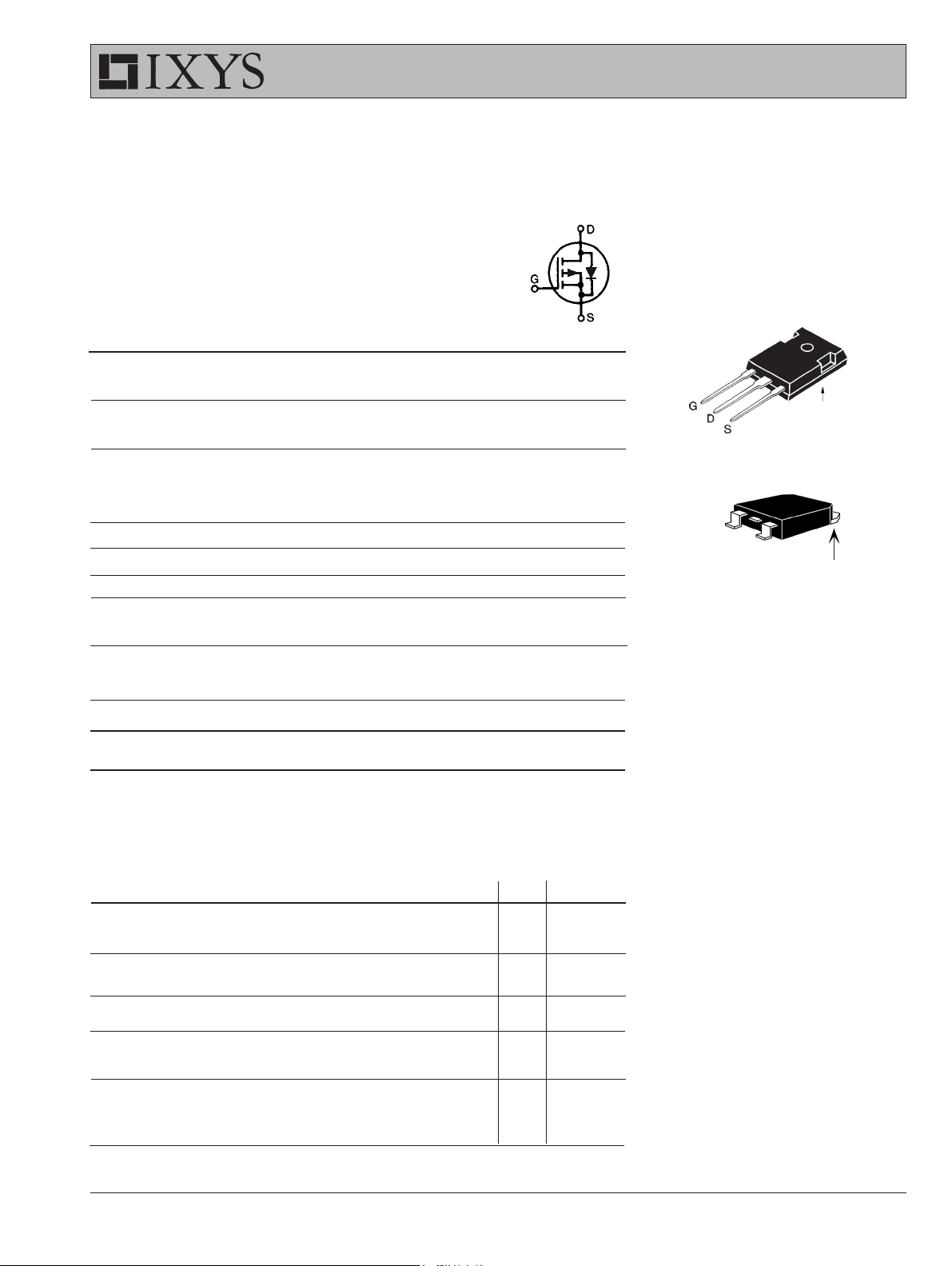
TO-247 (IXTH)
TO-268 (IXTT)
G = Gate, D = Drain,
S = Source, TAB = Drain
Features
= -500 V
= -8 A
= 1.2
G
S
ΩΩ
Ω
ΩΩ
D (TAB)
D (TAB)
• International standard packages
• Low R
HDMOSTM process
DS (on)
• Rugged polysilicon gate cell structure
• Unclamped Inductive Switching (UIS)
rated
• Low package inductance (<5 nH)
- easy to drive and to protect
Symbol Test Conditions Characteristic Values
(TJ = 25°C, unless otherwise specified)
min. typ. max.
V
DSS
V
GS(th)
I
GSS
I
DSS
R
DS(on)
© 2005 IXYS All rights reserved
VGS= 0 V, ID = -250 µA -500 V
BV
Temperature Coefficient 0.054 %/K
DSS
VDS= VGS, ID = -250 µA -3.0 -5.0 V
V
Temperature Coefficient -0.122 %/K
GS(th)
VGS= ±20 VDC, VDS = 0 ±100 nA
VDS= 0.8 • V
VGS= 0 V TJ = 125°C-1mA
VGS= -10 V, ID = 0.5 • I
R
Temperature Coefficient 0.6 %/K
DS(on)
DSS
TJ =25°C -200 µA
7P50 1.5 Ω
D25
8P50 1.2 Ω
Applications
• High side switching
• Push-pull amplifiers
• DC choppers
• Automatic test equipment
Advantages
• Easy to mount with 1 screw
(isolated mounting screw hole)
• Space savings
• High power density
DS94534F(02/05)
Page 2
IXTH 8P50
IXTT 8P50
Symbol Test Conditions Characteristic Values
(TJ = 25°C, unless otherwise specified)
min. typ. max.
g
C
C
C
t
t
t
t
Q
Q
Q
R
R
fs
iss
oss
rss
d(on)
r
d(off)
f
g(on)
gs
gd
thJC
thCS
VDS= -10 V; ID = I
VGS= 0 V, VDS = -25 V, f = 1 MHz 450 pF
VGS= -10 V, VDS = 0.5 V
RG = 4.7 Ω (External) 35 ns
VGS= -10 V, VDS = 0.5 V
(TO-247) 0.25 K/W
, pulse test 4 5 S
D25
3400 pF
175 pF
33 ns
DSS ID
= 0.5 I
D25
27 ns
35 ns
130 nC
DSS ID
= 0.5 I
D25
32 nC
64 nC
0.7 K/W
Source-Drain Diode Characteristic Values
(TJ = 25°C, unless otherwise specified)
Symbol Test Conditions min. typ. max.
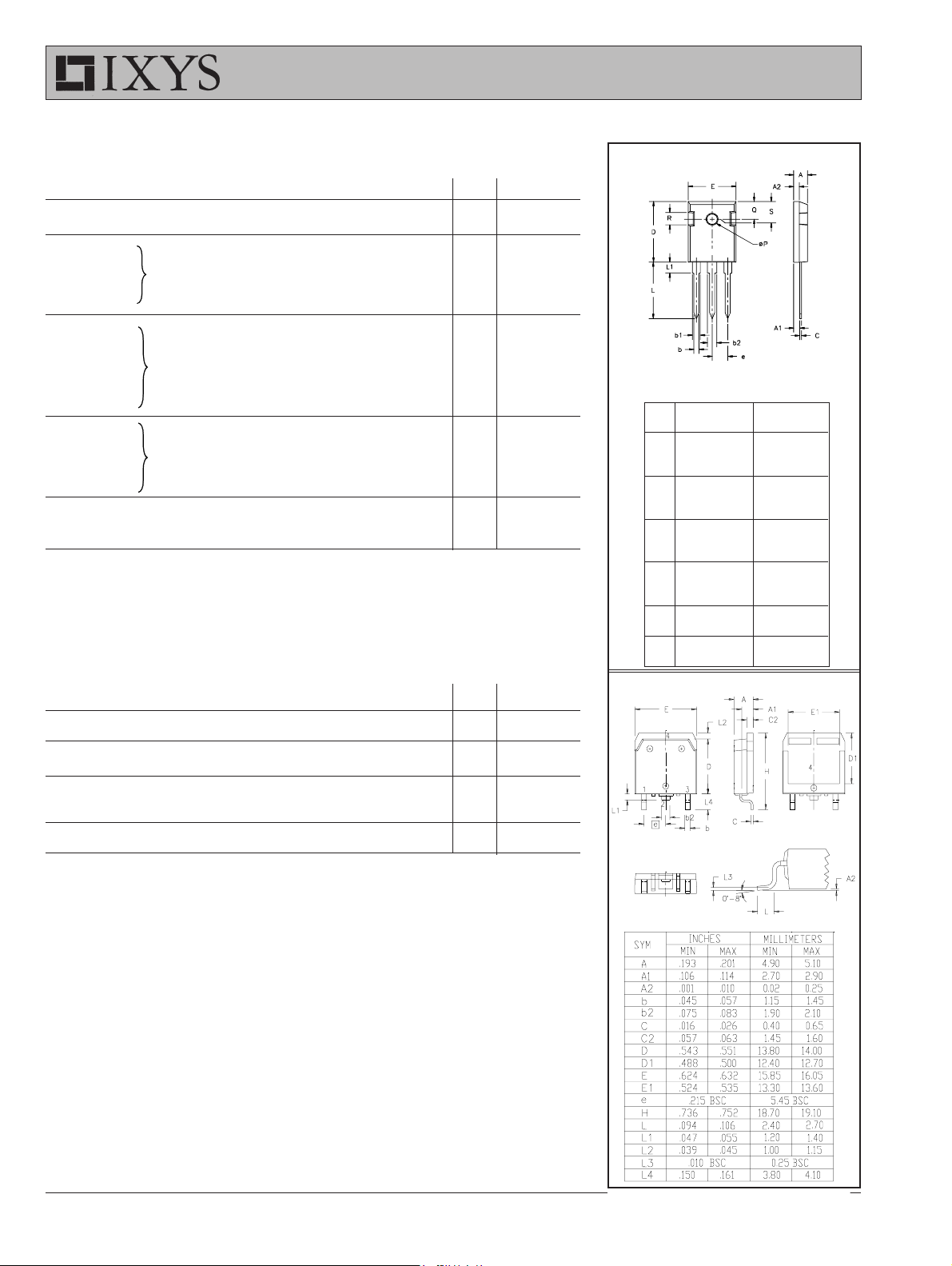
TO-247 (IXTH) Outline
1 2 3
Terminals: 1 - Gate 2 - Drain
3 - Source Tab - Drain
Dim. Millimeter Inches
Min. Max. Min. Max.
A 4.7 5.3 .185 .209
A
2.2 2.54 .087 .102
1
A22.2 2.6 .059 .098
b 1.0 1.4 .040 .055
b
1.65 2.13 .065 .084
1
b22.87 3.12 .113 .123
C .4 .8 .016 .031
D 20.80 21.46 .819 .845
E 15.75 16.26 .610 .640
e 5.20 5.72 0.205 0.225
L 19.81 20.32 .780 .800
L1 4.50 .177
∅P 3.55 3.65 .140 .144
Q 5.89 6.40 0.232 0.252
R 4.32 5.49 .170 .216
S 6.15 BSC 242 BSC
TO-268 (IXTT) Outline
I
S
I
SM
V
SD
t
rr
VGS= 0 -8 A
Repetitive; pulse width limited by T
JM
-32 A
IF = IS, VGS = 0 V, -3 V
Pulse test, t ≤ 300 µs, duty cycle d ≤ 2 %
IF = IS, di/dt = 100 A/µs 400 ns
IXYS reserves the right to change limits, test conditions, and dimensions.
IXYS MOSFETs and IGBTs are covered by 4,835,592 4,931,844 5,049,961 5,237,481 6,162,665 6,404,065 B1 6,683,344 6,727,585
one or moreof the following U.S. patents: 4,850,072 5,017,508 5,063,307 5,381,025 6,259,123 B1 6,534,343 6,710,405B2 6,759,692
4,881,106 5,034,796 5,187,117 5,486,715 6,306,728 B1 6,583,505 6,710,463 6771478 B2
 Loading...