

Page 1
Advance Technical Information
TrenchMV
TM
IXTF250N075T
Power MOSFET
(Electrically Isolated Back Surface)
N-Channel Enhancement Mode
Avalanche Rated
Symbol Test Conditions Maximum Ratings
V
DSS
V
DGR
V
GSM
I
D25
I
L
I
DM
I
AR
E
AS
TJ= 25°C to 175°C 75 V
TJ= 25°C to 175°C; RGS = 1 MΩ 75 V
Transient ± 20 V
TC= 25°C 140 A
Package Current Limit, RMS (75 A per lead) 150 A
TC= 25°C, pulse width limited by T
JM
560 A
TC= 25°C 40 A
TC= 25°C 1.5 J
V
I
D25
R
DSS
DS(on)
=75 V
= 140 A
4.44.4
≤≤
≤
4.4 m
≤≤
4.44.4
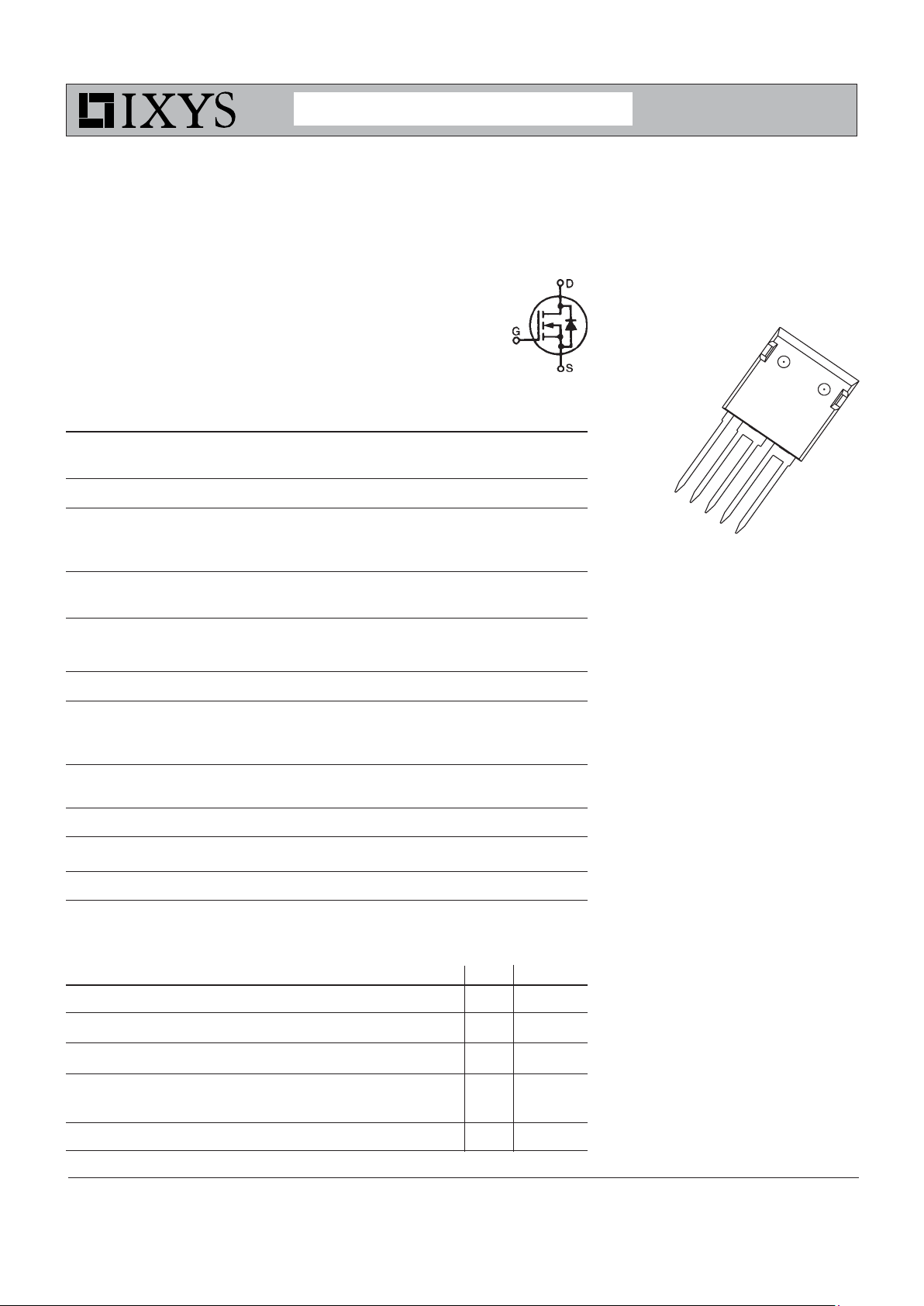
ISOPLUS i4-PakTM (5-lead) (IXTF)
G
S
S
D
D
G = Gate D = Drain
S = Source
ΩΩ
Ω
ΩΩ
dv/dt IS≤ IDM, di/dt ≤ 100 A/ms, VDD ≤ V
DSS
3 V/ns
TJ≤ 175°C, RG = 3.3 W
P
T
T
T
T
T
V
F
D
J
JM
stg
L
SOLD
ISOL
C
TC= 25°C 200 W
-55 ... +175 °C
175 °C
-55 ... +175 °C
1.6 mm (0.062 in.) from case for 10 s 300 °C
Plastic body for 10 seconds 260 ° C
50/60 Hz, t = 1 minute, I
< 1 mA, RMS 2500 V
ISOL
Mounting force 20..120/4.5..25 N/lb.
Weight 6g
Features
Ultra-low On Resistance
Unclamped Inductive Switching (UIS)
rated
Low package inductance
- easy to drive and to protect
175 °Χ Οπερατινγ Τεμπερατυρε
Advantages
Easy to mount
Space savings
High power density
Applications
Automotive
Symbol Test Conditions Characteristic Values
(TJ = 25°C unless otherwise specified) Min. Typ. Max.
BV
V
I
GSS
I
DSS
DSS
GS(th)
VGS= 0 V, ID = 250 μA75V
VDS= VGS, ID = 250 μA 2.0 4.0 V
VGS= ± 20 V, VDS = 0 V ± 200 nA
VDS= V
DSS
5 μA
- Motor Drives
- 42V Power Bus
- ABS Systems
DC/DC Converters and Off-line UPS
Primary Switch for 24V and 48V
Systems
High Current Switching
Applications
VGS= 0 V TJ = 150°C 25 0 μA
R
DS(on)
© 2007 IXYS CORPORATION All rights reserved
VGS= 10 V, ID = 50 A, Notes 1, 2 4.4mΩ
DS99745 (01/07)
Page 2
IXTF250N075T
Symbol Test Conditions Characteristic Values
g
C
C
C
t
t
t
t
Q
Q
Q
R
R
fs
iss
oss
rss
d(on)
r
d(off)
f
g(on)
gs
gd
thJC
thCH
(T
VDS= 10 V; ID = 60 A, Note 1 75 122 S
VGS = 0 V, VDS = 25 V, f = 1 M Hz 1330 pF
VGS = 10 V, VDS = 0.5 V
DSS
RG = 3.3 W (External) 58 ns
VGS= 10 V, VDS = 0.5 V
, ID = 25 A 50 nC
DSS
= 25°C unless otherwise specified)
J
Min. Typ. Max.
9900 pF
285 pF
32 ns
, ID = 50 A 50 ns
45 ns
200 nC
60 nC
0.75 °C/W
0.15 °C/W
Source-Drain Diode Characteristic Values
T
Symbol Test Conditions Min. Typ. Max.
= 25°C unless otherwise specified)
J
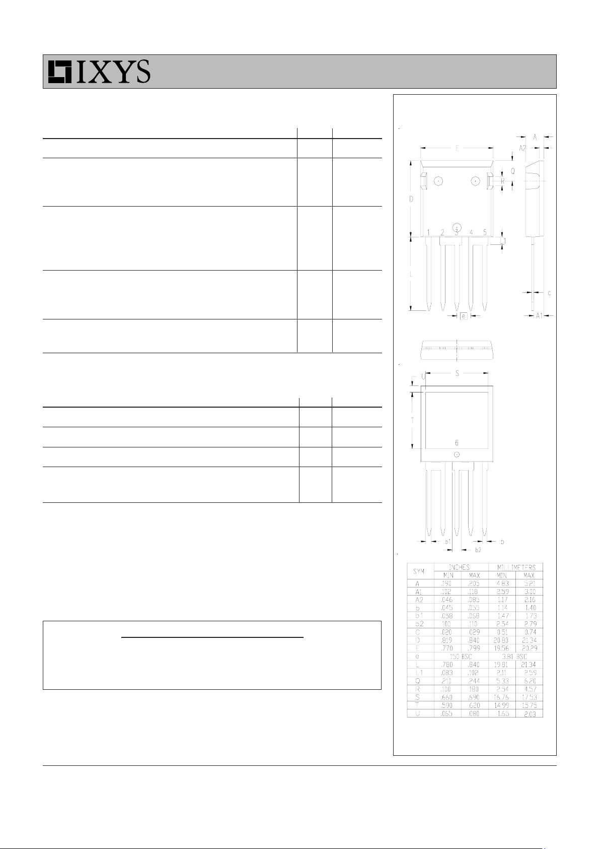
ISOPLUS i4-PakTM (5-Lead)
(IXTF) Outline
I
S
I
SM
V
SD
t
rr
VGS = 0 V 150 A
Pulse width limited by T
JM
560 A
IF = 50 A, VGS = 0 V, Note 1 1.0 V
IF = 25 A, -di/dt = 100 A/μs50ns
VR = 25 V, VGS = 0 V
Notes: 1. Pulse test: t ≤ 300 μs, duty cycled ≤ 2 %;
2. Drain and Source Kelvin contacts must be located less than 5 mm
from the plastic body.
ADVANCE TECHNICAL INFORMATION
The product presented herein is under development. The Technical Specifications offered
are derived from a subjective evaluation of the design, based upon prior knowledge and
experience, and constitute a "considered reflection" of the anticipated result. IXYS reserves
the right to change limits, test conditions, and dimensions without notice.
Leads:
1. Gate;
2, 3.
Source;
4, 5. Drain
6. Isolated.
All leads and tab are tin plated.
IXYS reserves the right to change limits, test conditions, and dimensions.
IXYS MOSFETs and IGBTs are covered by 4,835,592 4,931,844 5,049,961 5,237,481 6,162,665 6,404,065 B1 6,683,344 6,727,585 7,005,734 B2
one or moreof the following U.S. patents: 4,850,072 5,017,508 5,063,307 5,381,025 6,259,123 B1 6,534,343 6,710,405B2 6,759,692 7,063,975 B2
4,881,106 5,034,796 5,187,117 5,486,715 6,306,728 B1 6,583,505 6,710,463 6771478 B2 7,071,537
 Loading...