

Page 1
1:0321
1:03 51
Negative Voltage Hot Swap Controller
with Active Power Filter
Features
Live Insertion and Removal Power Manager
Adjustable Power-on slew rate
Autodetect of Load Open Circuit or -VIN
Disconnection
Controlled Time-Delay
Operates from 9 V to External MOSFET Voltage
Limit
Fault Indication Output (microprocessor reset).
Board Insertion/Removal Detector Input
Protection During Turn-On
Low frequency Power Active Filter
Adjustable Electronic Circuit Breaker
Vin undervoltage with GSNSin input
Applications
Arcless card insertion and removal
Central Office Switching Hardware
Circuit Boards From -48 V Distributed Power
Supplies
Circuit Board Power Manager and Noise Filter
Circuit Board Hot Swap Protector and Manager
Electronic Circuit Breaker
Wireless Local Loop Antennas
Cable TV Antenna
Description
The IXHQ100 is a live insertion and removal hot swap
controller with a built-in power noise filter. It incorporates all the active circuitry necessary to protect circuit
boards during live insertion or removal (insertion or
removal when the system power is active). Additionally,
the IXHQ100 incorporates two unique features: power
active filter for powerline noise suppression and power
auto-disconnect detector which eliminates the need of
additional staggered pins.
The IXHQ100 shunt regulator ensures a wide operating
voltage range (with the external MOSFET breakdown
voltage as limit). The active power filter reduces power
source output impedance, producing "clean" load
power. The IXHQ100 allows continuous load current
rise adjustments, presettable maximum current limits,
and user selectable fault indication turn off times for
resetting µPs and other synchronous board level sys-
tems. For added flexibility, GSNSin pin is available to
implement either circuit board insertion/removal detection or ground detection.
US Patents Pending.
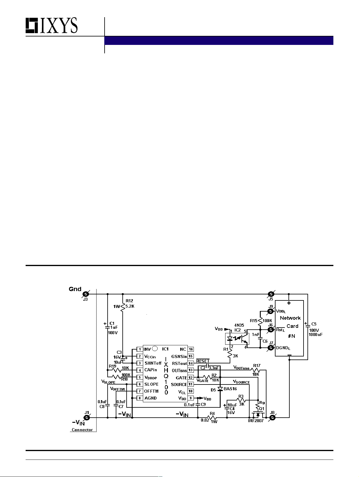
Typical Application with Auto-Disconnect Detector
CAUTION: These devices are
sensitvie to electrostatic discharge;
take caution when handling and
assembling this component.
Figure 1Figure 1
Figure 1
Figure 1Figure 1
IXYS reserves the right to change limits, test conditions and dimensions.
Copyright © IXYS CORPORATION 2000
www.ixys.com 98716 (08/14/00)
1
Page 2
Absolute Maximum RatingsAbsolute Maximum Ratings
Absolute Maximum Ratings
Absolute Maximum RatingsAbsolute Maximum Ratings
Symbol Symbol
Symbol
Symbol Symbol
Definition Definition
Definition
Definition Definition
Max. Rating Max. Rating
Max. Rating
Max. Rating Max. Rating
Pin DescriptionPin Description
Pin Description
Pin DescriptionPin Description
IXHQ 100PI
IXHQ 100SI
VCC-V
AGND
Voltage applied V
to AGND Shunt Off: -0.3 V to 16 V
CCin
Shunt On: -0.3 V to 14 V
Shunt On for 10 seconds 14V to 16 V
All other pins except V
I
VDD
T
JM
T
J0
T
stg
I
DD
Electrical CharacteristicsElectrical Characteristics
Electrical Characteristics
Electrical CharacteristicsElectrical Characteristics
Unless otherwise noted, TA = 25 oC; -VIN= 48 V, AGND connected to -VIN, V
with respect to AGND. IXHQ100 configured as described in
SymbolSymbol
Symbol
SymbolSymbol
I
CC
VDD Load Current 60 mA
Maximum Junction Temperature 125 oC
Operating Temperature Range -40 oC to 85 oC
Storage Temperature Range -40 oC to 150 oC
Supply Current with Shunt On 25 mA
Parameter Parameter
Parameter
Parameter Parameter
Supply current VCC=12 V, V
DC
-0.3 V to V
Test Conditions
Test ConditionsTest Conditions
Test Conditions
Test ConditionsTest Conditions
SHUNToff
all outputs unloaded.
V
CCSHUNT
V
shunt regulation ICC forced to 10 mA 12 13.8 16 V
CC
voltage when shunt is off
V
THSHUNToff
SHUNToff input VCC = 15 V, monitor RST
threshold voltage
I
SHUNToff
SHUNToff input -1 0 1 µA
bias current
V
THINV
INV input VCC = 12 V, monitor RST
threshold voltage
R
INV
INV input 70 130 180 KΩ
resistance
V
THGSNS
GSNS sense input VCC = 12 V, monitor RST
threshold voltage
I
GSNSin
GSNSin input -2.6 -2.3 -2 µA
bias current
I
CAPin
V
R
VDROP
VDROP
CAPin input bias current -1 0 1 µA
Active filter offset voltage 0.7 0.9 1.1 V
V
input resistance 50 70 90 KΩ
DROP
+ 0.3 V
CCin
SHUNToff
.
= 5 V, V
= 12 V, V
CC
= 12 V. All voltage measurements
GSNSin
MinMin
Min
MinMin
TypTyp
Typ
TypTyp
MaxMax
Max
MaxMax
Units Units
Units
Units Units
= VCC,23mA
OUT
OUT
OUT
1 1.5 2 V
6810V
4.5 5.8 6 V
I
SLOPE
R
SLOPEDCHG
I
OFFTM
R
OFFTMCHG
V
THOFFTM
V
CL
SLOPE capacitor V
charging current V
SLOPE capacitor V
discharge resistance V
OFFTM capacitor V
charging current V
= 5 V, V
OFFTM
= 5 V
CAPin
= 5 V, IVT = V
DROP
= 0 V, V
SOURCE
= 5 V, V
DROP
= 5 V
CAPin
= 0 V 70 85 110 mA
GSOURCE
CC
= 5 V
CAPin
= 0 V 80 100 120 mA
SOURCE
90 200 Ω
OFFTM capacitor 111 200 Ω
discharge resistance
OFFTM input threshold OFFTM input voltage when SLOPE 3.8 4.5 5.5 V
voltage input voltage starts its ramp
Overcurrent threshold bias voltage 90 125 150 mV
2
Page 3
Electrical Characteristics Electrical Characteristics
Electrical Characteristics (continued)
Electrical Characteristics Electrical Characteristics
SymbolSymbol
Symbol
SymbolSymbol
Parameter Parameter
Parameter
Parameter Parameter
Test ConditionsTest Conditions
Test Conditions
Test ConditionsTest Conditions
MinMin
Min
MinMin
IXHQ 100PI
IXHQ 100SI
TypTyp
Typ
TypTyp
MaxMax
Max
MaxMax
Units Units
Units
Units Units
R
VCL
t
OC
VCL bias resistance 4 6 10 kΩ
Overcurrent detection V
to GATE output delay V
= 0 V; V
CAPin
input is a step at t = 0s
SOURCE
OUTsns
= 5 V 20 30 ms
from 0 V to 200 mV
dv
/dt GATE output slew rate C
GATE
V
GATE
Maximum GATE V
output voltage V
I
GATE
I
GATE
GATE pull-up current Gate drive on, V
GATE pull-down Gate drive off 10 20 mA
current V
V
DD
VDD regulator output 3.3K Resistive load 5 5.75 6.5 V
= 100 nF 0.5 0.8 1.1 V/ms
SLOPE
CAPin
OUTsns
GATE
= 0 V; R
= 5 V
= 10 V
= 10 KΩ 13.8 15 V
load
= 0 V -15 -10 mA
GATE
Voltage between VDD output and AGND
I
RSTout
t
RST
V
ad
RSTout drive current Force V
=1 V during fault condition 2.4 3 3.6 mA
RSTout
RST pulse width 200 500 1000 ns
Auto-Detect threshold Gate drive on; ramp V
; monitor -10 12 20 mV
OUTsns
RST until it pulses.
Note 1: Operating the device beyond parameters with listed “absolute maximum ratings” may cause permanent damage to the
device. Typical values indicate conditions for which the device is intended to be functional, but do not guarantee specific
performance limits. The guaranteed specifications apply only for the test conditions listed. Exposure to absolute maximum
rated conditions for extended periods may affect device reliability.
Note2: All voltages are relative to ground unless otherwise specified.
Typical Performance CharacteristicsTypical Performance Characteristics
Typical Performance Characteristics
Typical Performance CharacteristicsTypical Performance Characteristics
Graph 1: Icc vs. TemperatureGraph 1: Icc vs. Temperature
Graph 1: Icc vs. Temperature
Graph 1: Icc vs. TemperatureGraph 1: Icc vs. Temperature
2.18
2.16
2.14
2.12
2.10
2.08
2.06
Icc (mA)
2.04
2.02
2.00
1.98
1.96
-60 -40 -20 0 20 40 60 80 100
Temperature (oC)
Graph 2: Regulator Output Voltage vs. TemperatureGraph 2: Regulator Output Voltage vs. Temperature
Graph 2: Regulator Output Voltage vs. Temperature
Graph 2: Regulator Output Voltage vs. TemperatureGraph 2: Regulator Output Voltage vs. Temperature
6.0
5.9
5.8
5.7
5.6
5.5
Regulator Output Voltage (V)
5.4
-60 -40 -20 0 20 40 60 80 100
Temperature (oC)
3
Page 4

IXHQ 100PI
IXHQ 100SI
Graph 3: SLOPE Pin current vs. TemperatureGraph 3: SLOPE Pin current vs. Temperature
Graph 3: SLOPE Pin current vs. Temperature
Graph 3: SLOPE Pin current vs. TemperatureGraph 3: SLOPE Pin current vs. Temperature
94
92
90
88
86
84
82
80
Slope Current (uA)
78
76
-60 -40 -20 0 20 40 60 80 100
Temperature (oC)
Graph 5: Vcc Shunt Voltage vs. TemperatureGraph 5: Vcc Shunt Voltage vs. Temperature
Graph 5: Vcc Shunt Voltage vs. Temperature
Graph 5: Vcc Shunt Voltage vs. TemperatureGraph 5: Vcc Shunt Voltage vs. Temperature
14.4
14.2
Graph 4: OFFTM Threshold Voltage vs. TemperatureGraph 4: OFFTM Threshold Voltage vs. Temperature
Graph 4: OFFTM Threshold Voltage vs. Temperature
Graph 4: OFFTM Threshold Voltage vs. TemperatureGraph 4: OFFTM Threshold Voltage vs. Temperature
6
5
4
OFFTM Threshold Voltage (V)
3
-60 -40 -20 0 20 40 60 80 100
Temperature (oC)
Graph 6: Overcurrent Threshold Voltage vs. TemperatureGraph 6: Overcurrent Threshold Voltage vs. Temperature
Graph 6: Overcurrent Threshold Voltage vs. Temperature
Graph 6: Overcurrent Threshold Voltage vs. TemperatureGraph 6: Overcurrent Threshold Voltage vs. Temperature
136
134
132
14.0
13.8
13.6
ICC = 1mA
Vcc Shunt Voltage (V)
13.4
13.2
-60 -40 -20 0 20 40 60 80 100
Temperature (oC)
Graph 7: Supply Current vs. Shunt VoltageGraph 7: Supply Current vs. Shunt Voltage
Graph 7: Supply Current vs. Shunt Voltage
Graph 7: Supply Current vs. Shunt VoltageGraph 7: Supply Current vs. Shunt Voltage
60
50
40
30
20
130
128
126
124
Vcl Voltage (mV)
122
120
118
-60 -40 -20 0 20 40 60 80 100
Temperature (oC)
Graph 8: Vdrop Voltage vs. TemperatureGraph 8: Vdrop Voltage vs. Temperature
Graph 8: Vdrop Voltage vs. Temperature
Graph 8: Vdrop Voltage vs. TemperatureGraph 8: Vdrop Voltage vs. Temperature
1.00
0.98
0.96
0.94
0.92
0.90
10
Supply Current (mA)
0
4 6 8 10 12 14 16 18
Vshunt (V)
Vdrop Voltage (V)
0.88
0.86
0.84
-60 -40 -20 0 20 40 60 80 100
Temperature (oC)
4
Page 5

IXHQ 100PI
IXHQ 100SI
Graph 9: Gate Voltage vs. Supply VoltageGraph 9: Gate Voltage vs. Supply Voltage
Graph 9: Gate Voltage vs. Supply Voltage
Graph 9: Gate Voltage vs. Supply VoltageGraph 9: Gate Voltage vs. Supply Voltage
16
14
12
10
Gate Voltage (V)
8
6
0 20 40 60 80 100 120
Supply Voltage (V)
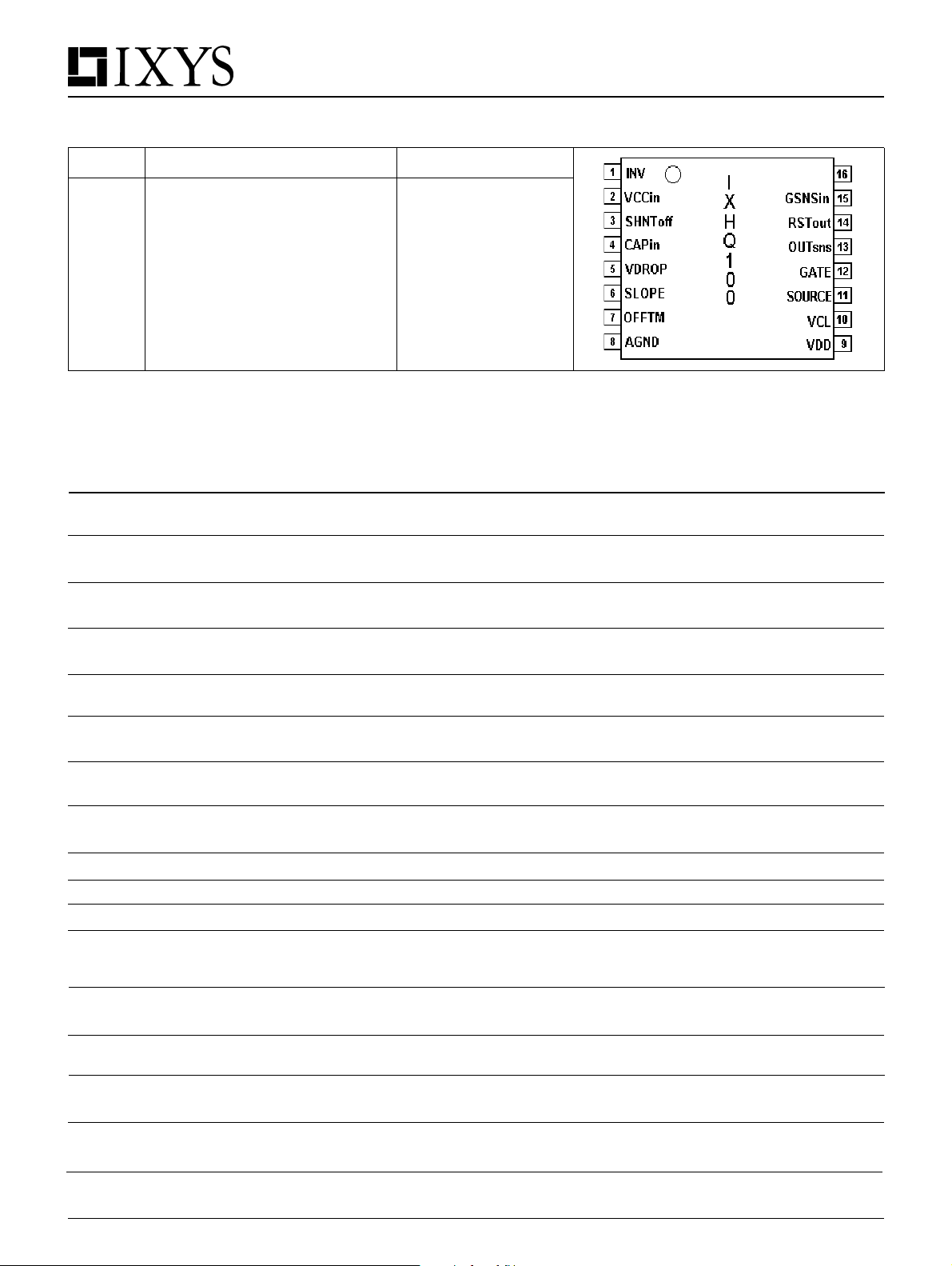
Pin DescriptionsPin Descriptions
Pin Descriptions
Pin DescriptionsPin Descriptions
PIN # SYMBOL FUNCTION DESCRIPTION
1
15 GSNSin
INV
Ground Sense
2 VCCin Supply Voltage Positive power-supply voltage input.
3 SHNToff Shunt Off
Active low-
4 CAPin
pass filter
capacitor input
5 VDROP
Active filter
offset voltage
6 SLOPE Slope input
7 OFFTM Off-time
8 AGND Ground The IXHQ100 system zero reference pin.
Invert
Input
Input
Graph 10: Typical Noise AttenuationGraph 10: Typical Noise Attenuation
Graph 10: Typical Noise Attenuation
Graph 10: Typical Noise AttenuationGraph 10: Typical Noise Attenuation
20
10
0
-10
-20
-30
-40
Attenuation (dB)
-50
-60
-70
1e+1 1e+2 1e+3 1e+4 1e+5 1e+6
Frequency (Hz)
The invert input controls GSNSin’s polarity. When
invert input is high compared to AGND, then GSNSin
low indicates an insertion/removal event. When invert
input is low, then GSNSin high indicates an
insertion/removal event.
The INV pin controls the polarity sense of this input.
A 3uA internal pull-up current source causes logic
high when there is no connection at this pin. With IN V
low or connected to AGND, a GSNSin low (or
connected to AGND) will keep RSTout and GATE
low, and the external power switch, Q1, off. A
disconnected GSNSin pin or when Vcc is applied to it
will allow normal operation
This pin serves to control the enabling of the shunt
circuit. When the pin is high compared to AGND, then
the shunt regulator is in off position. A low level at
this pin activates the shunt regulator.
The output of the power active filter tracks this pin.
Adding an external RC network matching the input
noise with respect to the 3db point of the filter could
reduce the noise to a minimum.
This pin sets the drop out MOSFET voltage across the
active filter.
This input controls the current slope during power up
and controls inrush currents. Adding external
capacitors to this pin allow regulation and adjustment
of the rate of the current slope.
The OFFTM pin sets the delay time between powerdown and restart of IXHQ100. Delay time can be
increased by adding external capacitors to this pin.
5
Page 6

Pin Descriptions Pin Descriptions
Pin Descriptions (continued)
Pin Descriptions Pin Descriptions
PIN # SYMBOL FUNCTION DESCRIPTION
9 VDDout
10 VCL
11 SOURCE
12 GATE Output Control voltage for driving external MOSFET.
13 OUTsns
14 RSTout Output Reset
16 NC N/A Not Connected
output voltage
threshold bias
Regulator
Overcurrent
voltage
Current input
sensor
Out sensor
signal
IXHQ 100PI
IXHQ 100SI
Regulator output voltage provides current to drive the
external circuits with respect to AGND.
Sets the overcurrent threshold bias voltage.
Input for sensing current through power device with
respect to AGND.
This signal senses the output voltage of the circuit.
A low at this pin indicates detection of an
insert/removal event or overcurrent detection.
IXHQ100 Logic DiaIXHQ100 Logic Dia
IXHQ100 Logic Dia
IXHQ100 Logic DiaIXHQ100 Logic Dia
gramgram
gram
gramgram
Figure 2Figure 2
Figure 2
Figure 2Figure 2
6
Page 7

IXHQ 100PI
IXHQ 100SI
DEVICE OPERADEVICE OPERA
DEVICE OPERA
DEVICE OPERADEVICE OPERA
TION*TION*
TION*
TION*TION*
A hot swap operation involves removal and
reinsertion of a device while the system using
it remains in operation. Such an operation
could cause external capacitors to draw currents high enough to disturb system operations
or even cause permanent damage to both the
device and the system.
The IXHQ100 is designed to prevent any disturbances or damage during such occurrences,
allowing the circuit board to be safely inserted
and removed from a live backplane. Capable of
operating under three modes, the chip also acts
as a power active noise filter and an auto-detect
circuit.
InserInser
Inser
InserInser
tion Prtion Pr
tion Pr
tion Prtion Pr
ocessocess
ocess
ocessocess
As the circuit board is inserted into the
backplane, physical connections should be
made to ground to discharge any electrostatic
voltage. The insertion process begins when
power and ground are supplied to the board
through pins on the blackplane.
Once power is applied, the IXHQ100 starts up
but does not immediately apply power to the
output load. The internal Power Up Reset logic
(see in Figure 2) turns on for 10 µs prior to any
other logic. This pulse goes through two NOR
gates and resets SRFF1 Flip Flop. Once SRFF1
is reset, the current source, I6, charges the
OFFTM pin at a rate proportional to the size of
the external capacitor, C7 (fig 1). During the time
the OFFTM pin is ramping from 0V to Vrf (~5V),
which is the T
V
stays at 0V. After T
SLOPE
, ,
, COMP1 keeps N3 ON so
, ,
off-delayoff-delay
off-delay
off-delayoff-delay
,,
, V
,,
off-delayoff-delay
off-delay
off-delayoff-delay
OFFTMOFFTM
OFFTM
OFFTMOFFTM
ecomes
greater than Vrf, and COMP1 goes low, driving
N3 to off state. I5 now starts to charge C1,
ramping +ve i/p of OA4. OA4 buffers V
SLOPE
and
sets the GATE output ramp.
It is assumed that when the circuit board is first
inserted into the backplane, the voltage across
the external load, V
, is zero. As V
load
SLOPE
rises,
its rate of increase determined by the value of
the external capacitor, C8 (figure1), and the
value of the internal current source, I5. V
rate of increase follows V
exceeds V
(figure 1) of the external power
thQ1
MOSFET, drain current I
rate of increase of I
of increase of V
SLOPE
is proportional to the rate
dQ1
, and is independent of the
As soon as V
SLOPE.
starts to flow. The
dQ1
GATE
GATE
's
size of C5 , the total filter capacitance of the
load. Note that this rate, which is directly
proportional to C7 and inversely proportional to
C8, could be adjusted . Similarly the Toff-delay
can be adjusted and is directly proportional to
the size of C7.
Normal OperationNormal Operation
Normal Operation
Normal OperationNormal Operation
With continuous –Vin applied, the IXHQ100
acts as an active power filter by modulating the
voltage drop across the external Power
MOSFET Vds so that any noise on –Vin is
cancelled by Vds.
The direct connection of IXHQ 100’s AGND pin
to –Vin allows the V
(internally set to ~750mV)
drop
to set the ~90% of the maximum peak noise
voltage reject by the IXHQ100. The internal
V
setting of ~750 mV allows 1.35 Vpp of
drop
noise rejection. Graph on page 5 illustrates the
level of ripple attenuation during normal
conditions. Notice that the noise rejection is very
high (~60db) between 400Hz to 40KHz, which is
optimal for most hot swap applications.
Flip-flop setting and resettingFlip-flop setting and resetting
Flip-flop setting and resetting
Flip-flop setting and resettingFlip-flop setting and resetting
The flip-flop, SRFF1 (fig 2), used in the IXHQ100,
is reset dominant. Hence when both S and R
inputs are driven high, the SRFF1 remains
reset. Under normal operation, S input becomes
high whenever OR1 output is high and R input
is low. In turn, OR1 goes high if any one of the
outputs of EXOR1, or COMP2, or COMP3
goes high.
EXOR1 output goes high if it detects the loss of
either Gnd or -Vin. If INV input is connected to
*Unless otherwise stated, all symbol and device references are referred to the logic diagram (Fig 2) on page 6
7
Page 8

IXHQ 100PI
IXHQ 100SI
Vcc, then GSNSin pin can be used to detect
the presence or absence of -Vin. If INV is
connected to AGND, then GSNSin pin can be
used to detect the presence or absence of
Gnd.
COMP2 output goes high whenever an
overcurrent or a short circuit condition is
detected. The inverting input to COMP2 is
connected to the VCL output pin which is
internally set at approximately 120mV. As
shown in Figure 1, one side of R4 is in series
with the source of Q1, the drain output of which
drives the load connected to J8. The return
side of R4 is connected to -Vin through J1. For
R4 = 0.02Ω, Q1 source currents greater than
6A will turn on COMP2 and will be considered
either an overcurrent or short circuit event.
COMP3 goes high whenever the voltage at
OUTsns with respect to AGND becomes less
than 0.1*VCL(approximately 12mV). This can
only occur if either the current drawn by the driven
load is less than 600mA (12mV/.02) or -VIN is
disconnected. This Auto-Disconnect technique
automatically detects load disconnections
without needing additional sensors.
Thus the SRFF1 will reset when one of the
following events occur:
1. Loss of AGND or -Vin.
2. Overcurrent or short circuit.
3. Auto-Disconnection
A valid S input into SRFF1 will immediately
drive its output, Q1, to high and will turn on both
N5 and N4. N5, an open drain output, will result
in RSTout being driven low. A current limiting
resistor, R1, in series with a 4N35 LED
connected to VDD (fig 1) can be used to
generate an isolated reset pulse. Turning on
N4 will discharge C7 and the internal 10pF
capacitor (fig 2). As soon as V
V
=~0.9V, COMP4 in Figure 2 will turn on
DROP
through NOR1 and NOR2, and resets SRFF1
drops below
OFFTM
with a high applied to its R input. This act will
then turn off both N5 and N4 and allow OFFTM
pin to initiate its positive ramp as a result of I6
charging the capacitors C7 (Figure 1) and C2
(Figure 2) connected to the OFFTM pin.
RestarRestar
Restar
RestarRestar
The IXHQ100 will automatically attempt to
restart once a disconnection and reconnection
is detected. Either PUR or COMP4 going high
will reset SRFF1 during normal operation of
the IXHQ100 (fig 2). Resetting SRFF1 turns off
N4 and N5, and the OFFTM pin ramps up in
response. During this ramp, as long as V
is less than Vrf=~4.5V, COMP1 will keep N3 on
and C1 (Figure 2) and C8 (Figure 1) discharged.
After T
then goes low, turning off N3. Now the SLOPE
pin is free to ramp up as a result of I5 charging
C1 (Figure 2) and C8 (Figure 1). The two unitygain buffers, OA4 and OA5, reflect V
GATE output pin during this positive ramp. As
soon as V
operation is resumed.
FF
ault Operationault Operation
F
ault Operation
FF
ault Operationault Operation
When the output load current is such that the
voltage drop across the current sense resistor
between the SOURCE pin and the AGND
exceeds VCL (internally set to ~120 mv), the
GATE output is driven low to turn off the external
Power MOSFET connected between the load
and -Vin. An external capacitor connected
between OFFTM pin and AGND pin determines
the off time T
on sequence of the external Power MOSFET
with a load voltage slope determined by the
size of the external capacitor that is connected
to the SLOPE pin.
ShorShor
Shor
ShorShor
When the IXHQ100 detects a short in the load,
a restart is automatically initiated. The GOUT
drops to zero and waits one T
SLOPE ramps up. As before, normal operation
is resumed.
t Operationt Operation
t Operation
t Operationt Operation
off-delay, VOFFTM
overcomes the V
GATE
off-delay.
t Cirt Cir
cuit Precuit Pre
t Cir
cuit Pre
t Cirt Cir
cuit Precuit Pre
OFFTM
is at Vrf, COMP1 output
at the
SLOPE
, normal
Q1th
IXHQ100 will restart the turn
ventionvention
vention
ventionvention
off-delay
before
8
Page 9

Package Outlines: 16 PIN TSSOP
IXHQ 100PI
IXHQ 100SI
Package Outlines: 16 PIN PDIP
Ordering InformationOrdering Information
Ordering Information
Ordering InformationOrdering Information
Part NumberPart Number
Part Number
Part NumberPart Number
IXHQ 100PI 16 PIN PDIP Industrial
IXHQ 100SI 16 PIN TSSOP Industrial
IXYS Corporation
3054 Bassett St; Santa Clara, CA 95054
Tel: 408-982-0700; Fax: 408-496-0670
e-mail: sales@ixys.com
Package TypePackage Type
Package Type
Package TypePackage Type
GradeGrade
Grade
GradeGrade
Edisonstrasse15 ; D-68623; Lampertheim
IXYS Semiconducotr GmbH
Tel: +49-6206-503-0; Fax: +49-6206-503627
e-mail: marcom@ixys.de
9
 Loading...