

Page 1
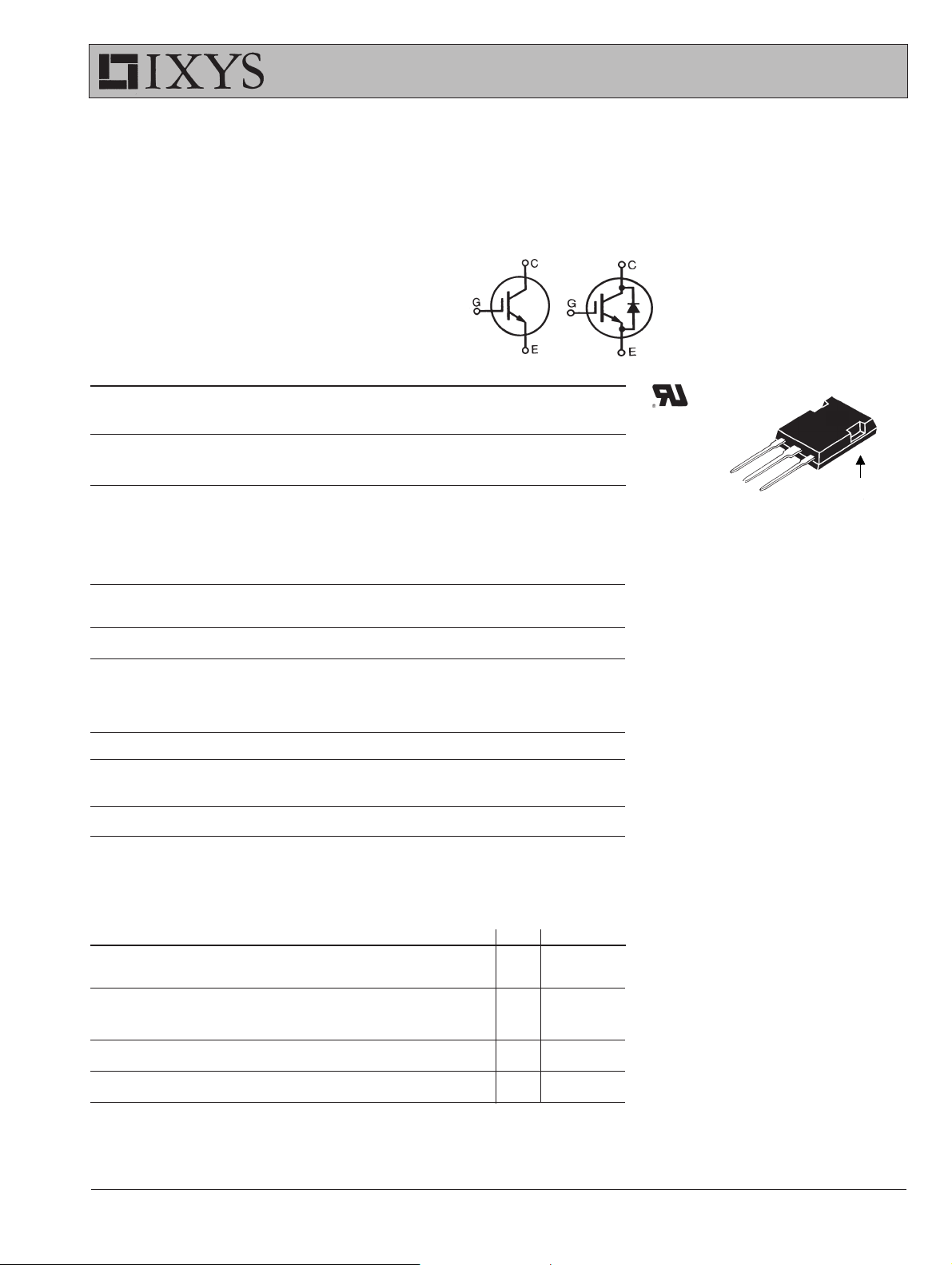
HiPerFASTTM IGBT
ISOPLUS247
TM
IXGR 40N60B2
IXGR 40N60B2D1
C2-Class High Speed IGBTs
(Electrically Isolated Back Surface)
Optimized for 10-25 KHz hard switching
and up to 150 KHz resonant switching
V
CES
I
C25
V
CE(sat)
t
fi typ
= 600 V
= 75 A
= 1.9 V
= 82 ns
Preliminary Data Sheet
Symbol Test Conditions Maximum Ratings
V
CES
V
CGR
V
GES
V
GEM
I
C25
I
C110
I
F110
I
CM
SSOA V
(RBSOA) Clamped inductive load @ ≤ 600 V
P
C
T
J
T
JM
T
stg
V
ISOL
TJ= 25°C to 150°C 600 V
TJ= 25°C to 150°C; RGE = 1 MΩ 600 V
Continuous ±20 V
Transient ±30 V
TC= 25°C60A
TC= 110°C33A
TC= 110°C (IXGR40N60B2D1) 25 A
TC= 25°C, 1 ms 200 A
= 15 V, TVJ = 125°C, RG = 10 Ω ICM = 80 A
GE
TC= 25°C 167 W
-55 ... +150 °C
-55 ... +150 °C
50/60 Hz RMS, t = 1m 2500 V
D1
150 °C
ISOPLUS247 (IXGR)
G = Gate, C = Collector,
E = Emitter
Features
z
z
z
z
z
Applications
Maximum lead temperature for soldering 300 °C
1.6 mm (0.062 in.) from case for 10 s
z
z
Weight 6g
z
z
z
Symbol Test Conditions Characteristic Values
V
I
CES
GE(th)
(TJ = 25°C, unless otherwise specified)
min. typ. max.
IC= 250 µA, VCE = V
VCE= V
VGE= 0 V TJ = 150°C1mA
CES
GE
TJ = 25°C50µA
3.0 5.0 V
Advantages
z
z
z
E153432
G
C
E
(ISOLATED TAB)
DCB Isolated mounting tab
Meets TO-247AD package Outline
High current handling capability
Latest generation HDMOSTM process
MOS Gate turn-on
- drive simplicity
Uninterruptible power supplies (UPS)
Switched-mode and resonant-mode
power supplies
AC motor speed control
DC servo and robot drives
DC choppers
Easy assembly
High power density
Very fast switching speeds for high
frequency applications
I
GES
V
CE(sat)
© 2004 IXYS All rights reserved
VCE= 0 V, VGE = ±20 V ±100 nA
IC= 30 A, VGE = 15 V TJ = 25°C 1.9 V
DS99162A(05/04)
Page 2
Symbol Test Conditions Characteristic Values
(T
= 25°C, unless otherwise specified)
J
min. typ. max.
IXGR 40N60B2
IXGR 40N60B2D1
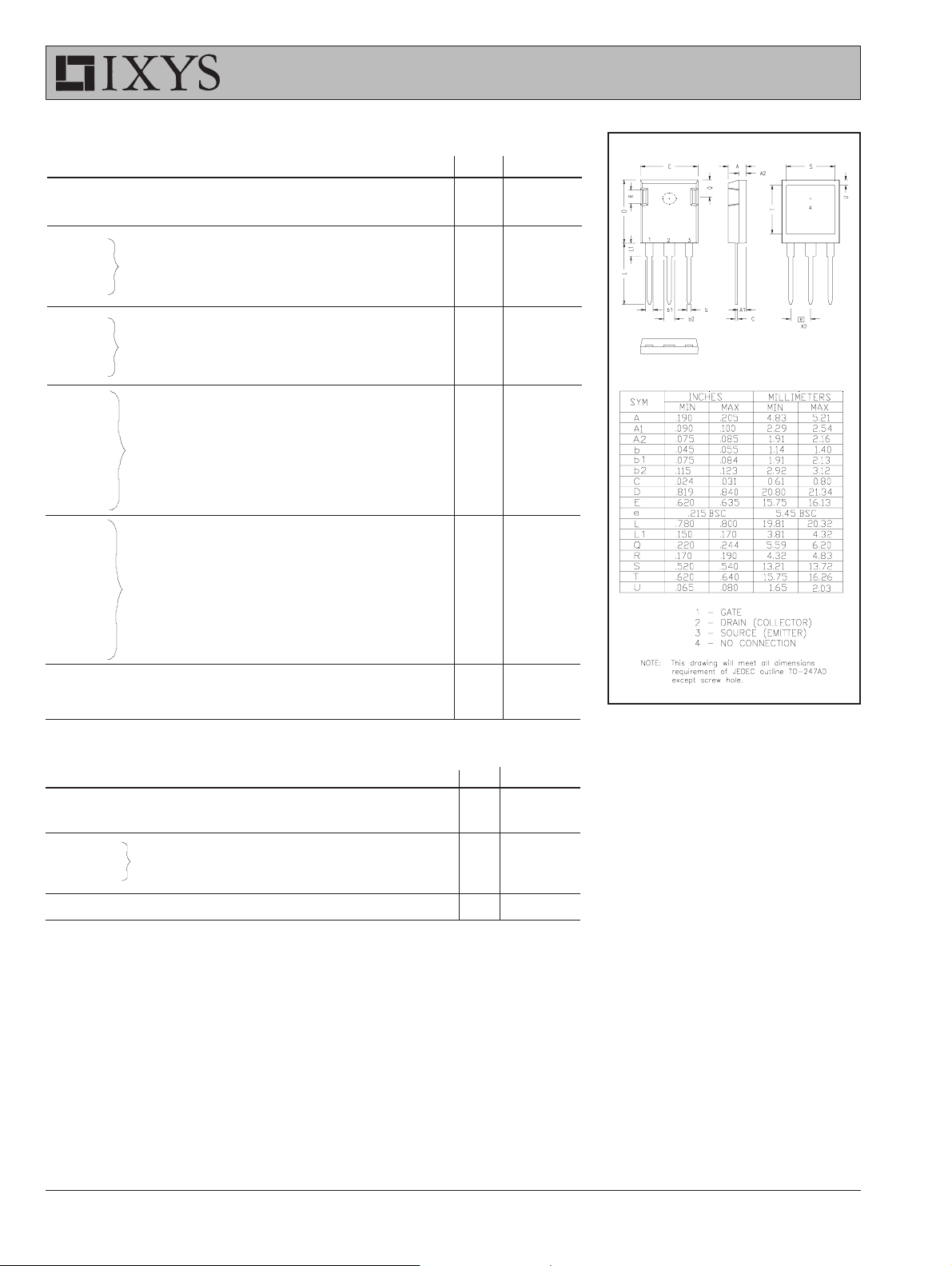
ISOPLUS 247 Outline
g
C
C
C
Q
Q
Q
t
t
t
t
E
t
t
E
t
t
E
R
R
fs
ies
oes
res
g
ge
gc
d(on)
ri
d(off)
fi
off
d(on)
ri
on
d(off)
fi
off
thJC
thCK
IC= 30 A; VCE = 10 V, 20 36 S
Pulse test, t ≤ 300 µs, duty cycle ≤ 2 %
2560 pF
VCE = 25 V, VGE = 0 V, f = 1 MHz 210 pF
54 pF
100 nC
IC = 30 A, VGE = 15 V, VCE = 300 V 15 nC
36 nC
18 ns
Inductive load, TJ = 25
IC = 30 A, VGE = 15 V
VCE = 400 V, RG = 3.3 Ω
°°
°C
°°
20 ns
130 200 ns
82 150 ns
0.4 0.8 mJ
18 ns
Inductive load, TJ = 125
IC = 30 A, VGE = 15 V
VCE = 400 V, RG = 3.3 Ω
°°
°C
°°
20 ns
0.3 mJ
240 ns
150 ns
1.10 mJ
0.75 K/W
0.15 K/W
Reverse Diode (FRED) Characteristic Values
= 25°C, unless otherwise specified)
(T
Symbol Test Conditions min. typ. max.
V
F
I
RM
t
rr
R
thJC
IXYS reserves the right to change limits, test conditions, and dimensions.
IXYS MOSFETs and IGBTs are covered by 4,835,592 4,931,844 5,049,961 5,237,481 6,162,665 6,404,065 B1 6,683,344 6,727,585
one or moreof the following U.S. patents: 4,850,072 5,017,508 5,063,307 5,381,025 6,259,123 B1 6,534,343 6,710,405B2
IF= 30 A, VGE = 0 V, Pulse test TJ =150°C 1.6 V
t ≤ 300 µs, duty cycle d ≤ 2 % 2.5 V
IF= 30 A, VGE = 0 V, -diF/dt =100 A/µs, TJ = 100°C4A
VR= 100 V TJ = 100°C 100 ns
IF= 1 A; -di/dt = 100 A/µs; VR = 30 V 25 ns
4,881,106 5,034,796 5,187,117 5,486,715 6,306,728 B1 6,583,505 6,710,463
J
0.9 1.1 K/W
Page 3
IXGR 40N60B2
IXGR 40N60B2D1
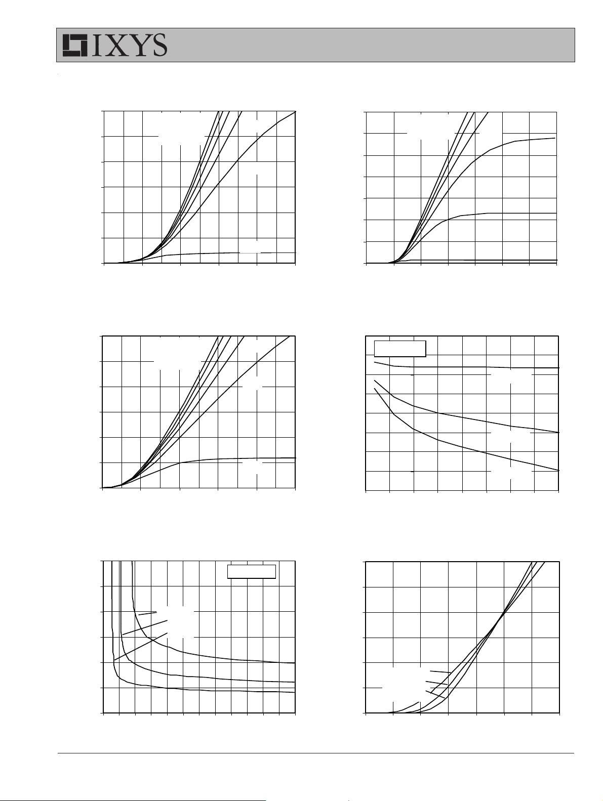
Fig. 1. Output Characte r is tics
@ 25 Deg. C
60
50
40
30
- Amperes
C
I
20
10
0
0.511.522.53
V
= 15V
GE
13V
11V
V
- Volts
C E
9V
7V
5V
Fig. 3. Output Characte r is tics
@ 125 Deg. C
60
50
40
V
= 15V
GE
13V
11V
9V
7V
Fig. 2. Extended Output Char acteristics
@ 25 deg. C
210
180
150
120
90
- Amperes
C
I
60
30
0
01234567
V
= 15V
GE
13V
V
C E
11V
9V
7V
5V
- Volts
Fig. 4. Depende nce of V
CE(sat)
Tem pe rature
1.4
1.3
1.2
1.1
VGE = 15V
IC = 60A
on
30
- Amperes
C
I
20
10
0
0.5 1 1.5 2 2. 5 3
VCE - Volts
Fig. 5. Collector -to-Em itte r Voltage
vs. Gate-to-Em itter voltage
4
T
J
3.5
3
2.5
- Volts
C E
V
2
1.5
IC = 60A
30A
15A
5V
= 25ºC
1.0
- Normalized
0.9
C E (s at)
V
0.8
0.7
0.6
-50 -25 0 25 50 75 100 125 150
IC = 30A
IC = 15A
TJ - Degrees Centigrade
Fig. 6. Input Adm ittance
180
150
120
90
- Amperes
C
I
60
30
TJ = 125ºC
25ºC
-40ºC
1
567891011121314151617
V
© 2004 IXYS All rights reserved
- Volts
G E
0
345678910
V
- Volts
G E
Page 4
IXGR 40N60B2
IXGR 40N60B2D1
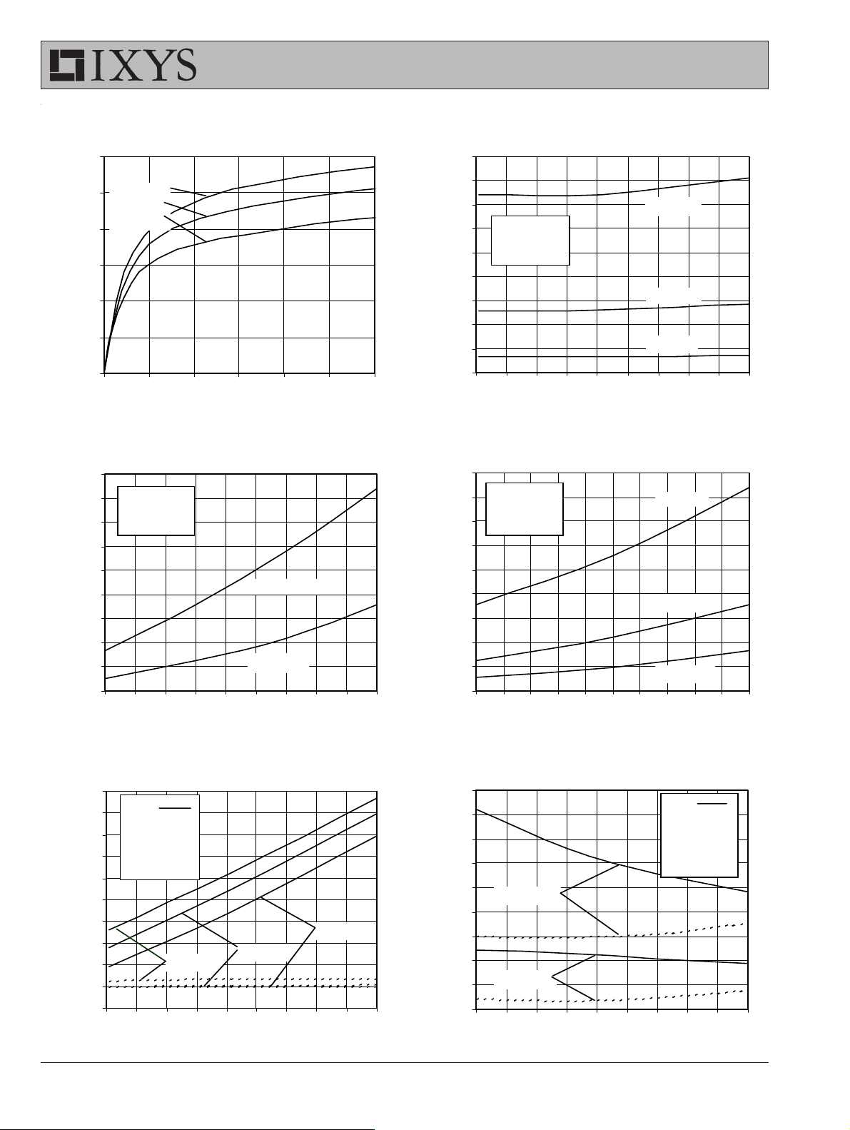
Fig. 7. Transconductance
60
TJ = -40ºC
50
25ºC
125ºC
40
30
- Siemens
f s
g
20
10
0
0 30 60 90 120 150 180
I C - A mperes
Fig. 9. Dependence of Turn-Off
En e r g y
2.7
2.4
2.1
1.8
1.5
1.2
- MilliJoules
off
E
0.9
0.6
0.3
RG = 3.3Ω
= 15V
V
GE
= 400V
V
CE
0
15 20 25 30 35 40 45 50 55 60
on I
c
TJ = 125ºC
TJ = 25ºC
I C - Amperes
Fig. 8. Dependence of Turn-Off
En e r g y o n R
3
2.7
2.4
TJ = 125ºC
= 15V
V
GE
V
= 400V
CE
3 6 9 1215 1821242730
- milliJoules
E
2.1
1.8
1.5
off
1.2
0.9
0.6
0.3
G
IC = 60A
IC = 30A
IC = 15A
R G - Ohms
Fig. 10. Dependence of Turn-Off
Energy on Temperature
2.7
2.4
2.1
1.8
1.5
1.2
- milliJoules
off
0.9
E
0.6
0.3
RG = 3.3 Ω
= 15V
V
GE
= 400V
V
CE
0
25 35 45 55 65 75 85 95 105 115 125
IC = 60A
IC = 30A
IC = 15A
TJ - Degrees Centigrade
Fig. 11. Dependence of Turn-Off
Switching Time on R
Switching Time - nanos econd
600
550
500
450
400
350
300
250
200
150
100
t
d(off)
tfi -
- - - - -
= 125ºC
T
J
V
= 15V
GE
= 400V
V
CE
IC = 60A
3 6 9 12151821242730
IC = 30A
G
IC = 15A
R G - Ohms
IXYS reserves the right to change limits, test conditions, and dimensions.
Fig. 12. Depende nce of Turn-Off
Switching Tim e
300
275
250
225
Switching Time - nanos econd
200
175
150
125
100
75
TJ = 125ºC
TJ = 25ºC
15 20 25 30 35 40 45 50 55 60
on I
t
V
I C - Amperes
c
t
d(off)
fi
R
= 3. 3Ω
G
V
GE
CE
- - - - - -
= 15V
= 400V
Page 5
IXGR 40N60B2
IXGR 40N60B2D1
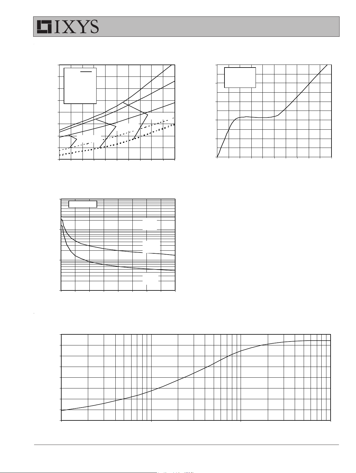
Fig. 13. Dependence of Turn-Off
Switching Tim e on Tem perature
275
t
d(off)
tfi -
- - - - -
= 3.3Ω
R
G
V
= 15V
GE
V
= 400V
CE
IC = 30A
IC = 60A
25 35 45 55 65 75 85 95 105 115 125
TJ - Degrees Centigrade
Switching Time - nanosec ond
250
225
200
175
150
125
100
75
Fig. 15. Capacitance
10000
1000
f = 1 MHz
C
IC = 15A
ies
Fig. 14. Gate Charge
15
V
= 300V
CE
= 30A
I
12
9
- Volts
6
G E
V
3
0
C
I
= 10m A
G
0 1020 3040 50 60708090100
Q G - nanoCoulombs
C
oes
100
Capacit ance - p F
C
res
10
0 5 10 15 20 25 30 35 40
V
C E
- Volts
Fig. 13. Maximum Transient Thermal Resistance
0.8
0.7
0.6
0.5
(ºC/W)
-
0.4
(th) J C
0.3
R
0.2
0.1
0
1 10 100 1000
Pulse Width - millis econds
© 2004 IXYS All rights reserved
Page 6
IXGR 40N60B2
IXGR 40N60B2D1
60
A
50
I
F
40
TVJ=150°C
30
TVJ=100°C
20
TVJ=25°C
10
0
0123
V
V
F
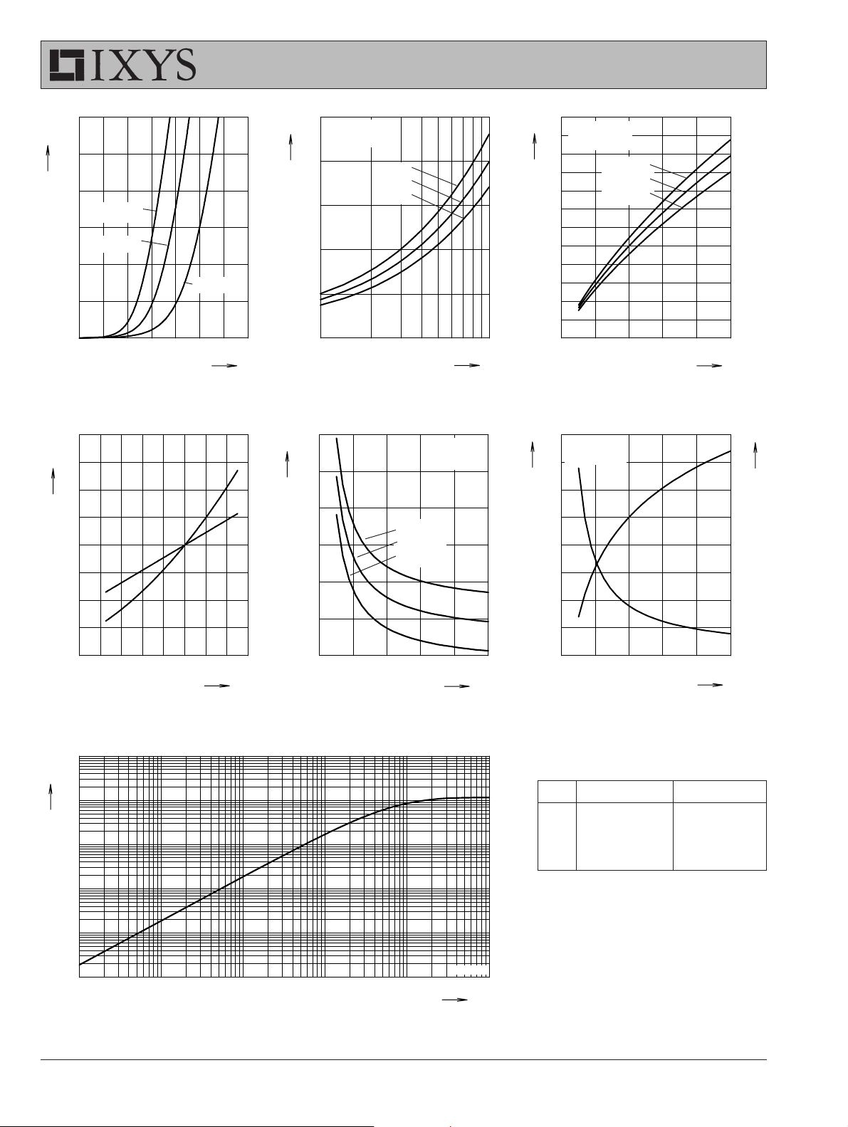
Fig. 17 Forward current IF versus V
2.0
1.5
K
f
1.0
I
RM
0.5
Q
r
I
RM
30
A
25
20
TVJ= 100°C
V
= 300V
R
IF= 60A
IF= 30A
IF= 15A
1000
Q
nC
800
r
600
TVJ= 100°C
V
= 300V
R
IF= 60A
= 30A
I
F
IF= 15A
15
400
10
200
0
100 1000
A/µs
-diF/dt
F
Fig. 18 Reverse recovery charge Q
versus -diF/dt
90
TVJ= 100°C
r
VR = 300V
ns
t
rr
80
5
0
200 600 10000 400 800
/dt
-di
F
Fig. 19 Peak reverse current I
versus -diF/dt
20
TVJ= 100°C
IF = 30A
V
V
FR
15
t
fr
V
FR
A/µs
RM
1.00
µs
t
fr
0.75
IF= 60A
IF= 30A
IF= 15A
10
0.50
70
5
0.25
0.0
0 40 80 120 160
°C
T
VJ
Fig. 20 Dynamic parameters Qr, I
versus T
VJ
RM
60
200 600 10000 400 800
/dt
-di
F
Fig. 21 Recovery time trr versus -diF/dt Fig. 22 Peak forward voltage VFR and
10
K/W
1
Z
thJC
0.1
0.01
0.001
0.0001
0.00001 0.0001 0.001 0.01 0.1 1
t
Fig. 23 Transient thermal resistance junction to case
IXYS reserves the right to change limits, test conditions, and dimensions.
A/µs
DSEP 2x31-06B
s
0
0 200 400 600 800 1000
A/µs
diF/dt
t
fr
Constants for Z
versus diF/dt
calculation:
thJC
iR
(K/W) ti (s)
thi
1 0.436 0.0055
2 0.482 0.0092
3 0.117 0.0007
4 0.115 0.0418
0.00
906
 Loading...