

Page 1
1 - 4
© 2000 IXYS All rights reserved
Symbol Test Conditions Maximum Ratings
V
CES
TJ= 25°C to 150°C 600 V
V
CGR
TJ= 25°C to 150°C; RGE = 1 MW 600 V
V
GES
Continuous ±20 V
V
GEM
Transient ±30 V
I
C25
TC= 25°C45A
I
C110
TC= 110°C26A
I
CM
TC= 25°C, 1 ms 120 A
SSOA V
GE
= 15 V, TVJ = 125°C, RG = 10 W ICM = 64 A
(RBSOA) Clamped inductive load, L = 100 mH @ 0.8 V
CES
P
C
TC= 25°C 140 W
T
J
-55 ... +150 °C
T
JM
150 °C
T
stg
-55 ... +150 °C
Maximum lead temperature for soldering 300 °C
1.6 mm (0.062 in.) from case for 10 s
V
ISOL
50/60 Hz, RMS, t = 1minute leads-to-tab 2500 V
Weight 6g
Symbol Test Conditions Characteristic Values
(TJ = 25°C, unless otherwise specified)
min. typ. max.
BV
CES
IC= 250 mA, VGE = 0 V 600 V
V
GE(th)
IC= 250 mA, VCE = V
GE
2.5 5 V
I
CES
VCE= 0.8 • V
CES
TJ = 25°C 200 mA
VGE= 0 V TJ = 150°C1mA
I
GES
VCE= 0 V, VGE = ±20 V ±100 nA
V
CE(sat)
IC= IT, VGE = 15 V (see note 1) 2.1 2.5 V
98651A (7/00)
IXGR 32N60C V
CE
= 600 V
I
C25
= 45 A
V
CE(sat)typ
= 2.1 V
t
fi typ
= 55 ns
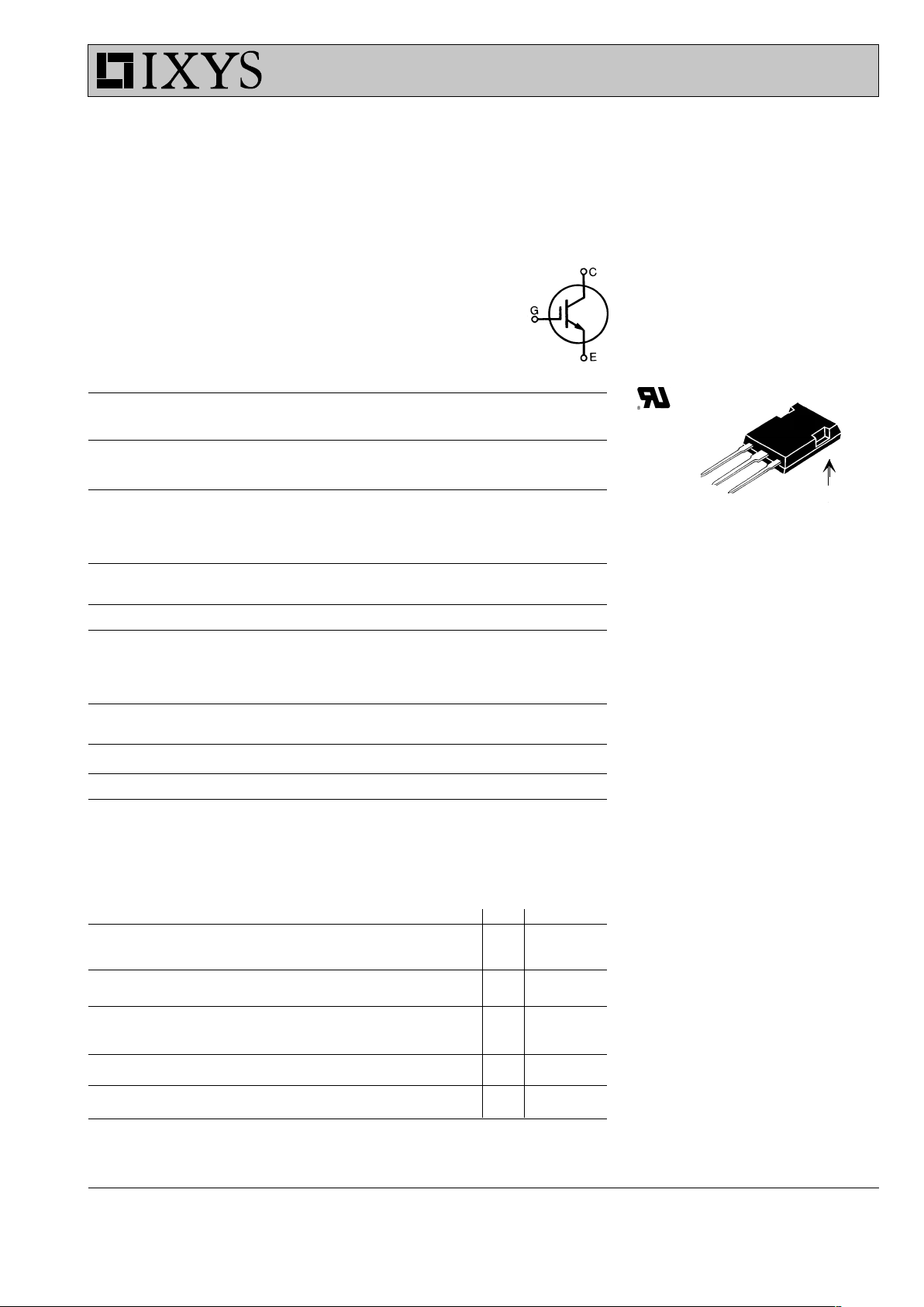
HiPerFASTTM IGBT
Lightspeed Series
ISOPLUS247TM package
(Electrically Isolated Back Side)
G = Gate, C = Collector,
E = Emitter
*Patent pending
ISOPLUS 247
TM
E153432
G
C
E
Isolated Backside*
Features
• DCB Isolated mounting tab
• Meets TO-247AD package Outline
• High current handling capability
• Latest generation HDMOS
TM
process
• MOS Gate turn-on
- drive simplicity
Applications
• Uninterruptible power supplies (UPS)
• Switched-mode and resonant-mode
power supplies
• AC motor speed control
• DC servo and robot drives
• DC choppers
Advantages
• Easy assembly
• High power density
• Very fast switching speeds for high
frequency applications
IXYS reserves the right to change limits, test conditions, and dimensions.
Page 2
2 - 4
© 2000 IXYS All rights reserved
Symbol Test Conditions Characteristic Values
(TJ = 25°C, unless otherwise specified)
min. typ. max.
g
fs
IC= IT; VCE = 10 V, 25 S
Pulse test, t £ 300 ms, duty cycle £ 2 %
C
ies
2700 pF
C
oes
VCE = 25 V, VGE = 0 V, f = 1 MHz 1 90 pF
C
res
50 pF
Q
g
110 nC
Q
ge
IC = IT, VGE = 15 V, VCE = 0.5 V
CES
22 nC
Q
gc
40 nC
t
d(on)
25 ns
t
ri
20 ns
t
d(off)
85 ns
t
fi
55 ns
E
off
0.32 mJ
t
d(on)
25 ns
t
ri
25 ns
E
on
0.30 mJ
t
d(off)
110 170 ns
t
fi
105 160 ns
E
off
0.85 1.25 mJ
R
thJC
0.90 K/W
R
thCK
0.15 K/W
Inductive load, TJ = 25°C
IC = IT, VGE = 15 V, L = 100 mH,
VCE = 0.8 V
CES
, RG = R
off
= 4.7 W
Remarks: Switching times may
increase for VCE (Clamp) > 0.8 • V
CES
,
higher TJ or increased R
G
Inductive load, TJ = 150°C
IC = IT, VGE = 15 V, L = 100 mH
V
CE
= 0.8 V
CES
, RG = R
off
= 4.7 W
Remarks: Switching times may
increase for V
CE
(Clamp) > 0.8 • V
CES
,
higher TJ or increased R
G
IXGR 32N60C
Note 1: IT = 32A
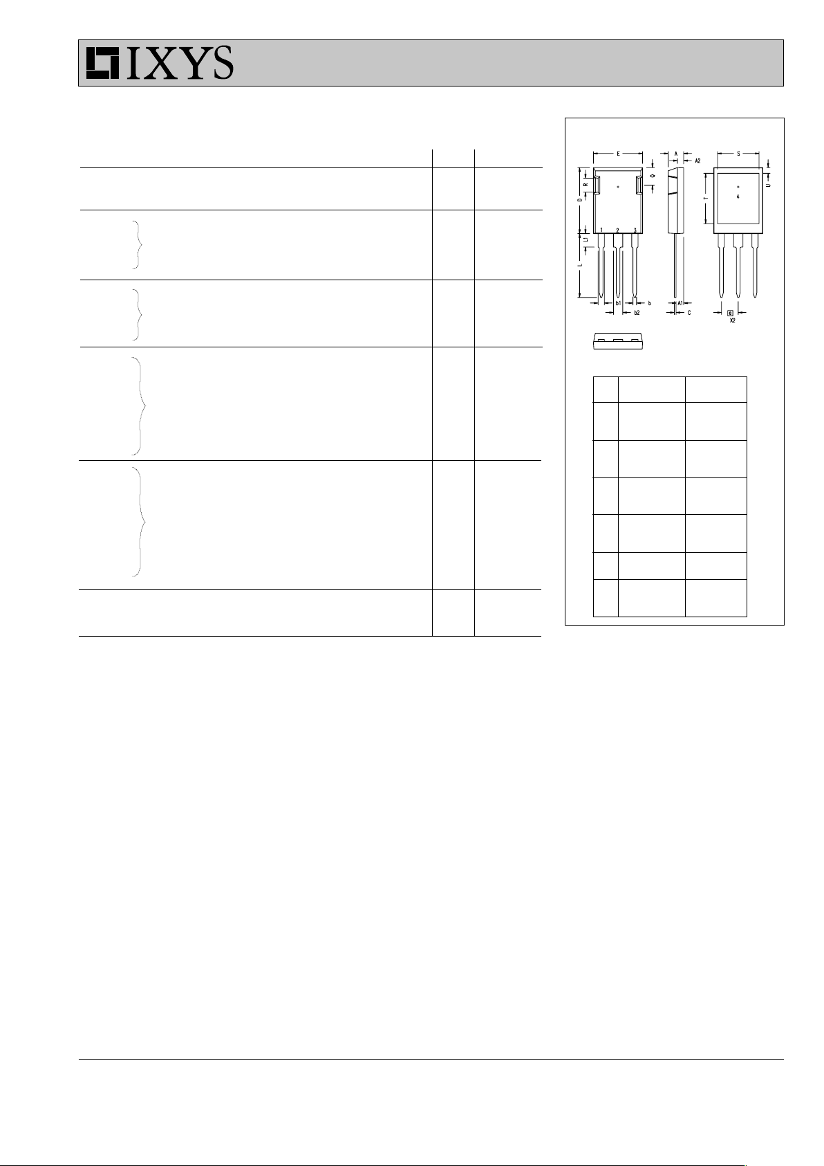
ISOPLUS 247 (IXGR) OUTLINE
Dim. Millimeter Inches
Min. Max. Min. Max.
A 4.83 5.21 .190 .205
A
1
2.29 2.54 .090 .100
A21.91 2.16 .075 .085
b 1.14 1.40 .045 .055
b
1
1.91 2.13 .075 .084
b22.92 3.12 .115 .123
C 0.61 0.80 .024 .031
D 20.80 21.34 .819 .840
E 15.75 16.13 .620 .635
e 5.45 BSC .215 BSC
L 19.81 20.32 .780 .800
L1 3.81 4.32 .150 .170
Q 5.59 6.20 .220 .244
R 4.32 4.83 .170 .190
S 13.21 13.72 .520 .540
T 15.75 16.26 .620 .640
U 1.65 3.03 .065 .080
1 Gate, 2 Drain (Collector)
3 Source (Emitter)
4 no connection
IXYS MOSFETS and IGBTs are covered by one or more of the following U.S. patents:
4,835,592 4,881,106 5,017,508 5,049,961 5,187,117 5,486,715
4,850,072 4,931,844 5,034,796 5,063,307 5,237,481 5,381,025
Page 3
3 - 4
© 2000 IXYS All rights reserved
VCE - Volts
012345
I
C
- Amperes
0
20
40
60
80
100
VCE - Volts
012345
I
C
- Amperes
0
20
40
60
80
100
VCE-Volts
0 5 10 15 20 25 30 35 40
Capacitance - pF
10
100
1000
10000
TJ - Degrees C
25 50 75 100 125 150
V
CE (sat)
- Normalized
0.50
0.75
1.00
1.25
1.50
VGE - Volts
345678910
I
C
- Amperes
0
20
40
60
80
100
VCE - Volts
0246810
I
C
- Amperes
0
40
80
120
160
200
13V
11V
9V
7V
V
CE
= 10V
VGE = 15V
13V
TJ = 25°C
VGE = 15V
TJ = 25°C
IC = 16A
I
C
= 32A
I
C
= 64A
T
J
= 125°C
f = 1Mhz
5V
5V
VGE = 15V
TJ = 25°C
TJ = 125°C
7V
9V
5V
7V
9V
VGE = 15V
13V
C
iss
C
oss
C
rss
11V
11V
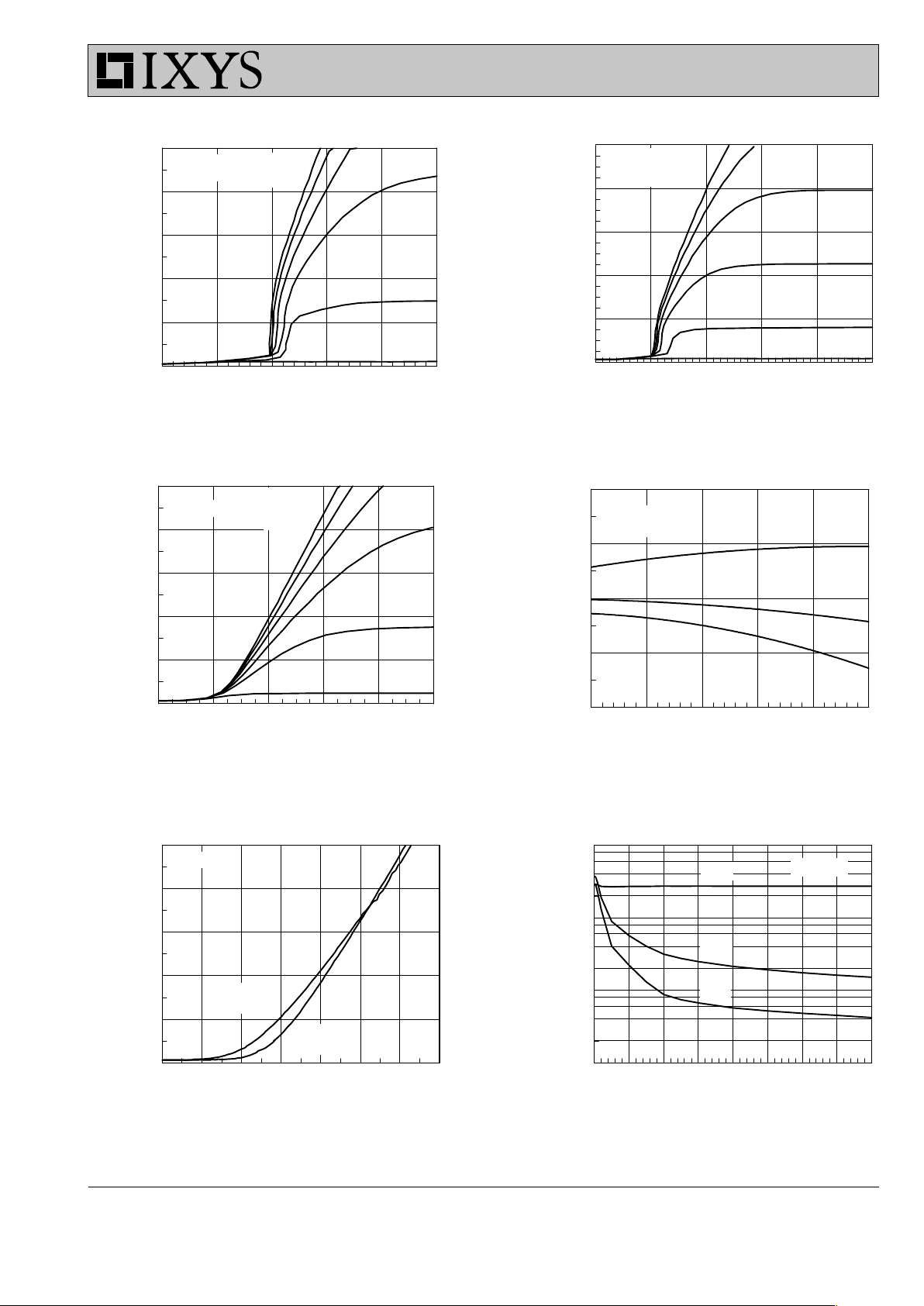
Fig. 1. Output Characteristics
Fig. 2. Extended Output Characteristics
Fig. 3. High Temperature Output Characteristics
Fig. 4. Temperature Dependence of V
CE(sat)
Fig. 5. Admittance Curves
Fig. 6. Capacitance Curves
IXGR 32N60C
Page 4
4 - 4
© 2000 IXYS All rights reserved
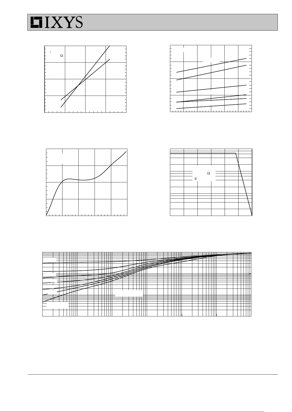
Fig. 11. Transient Thermal Resistance
IXGR 32N60C
Pulse Width - Seconds
0.00001 0.0001 0.001 0.01 0.1 1 10
Z
thJC
(K/W)
0.001
0.01
0.1
1
D=0.2
VCE - Volts
0 100 200 300 400 500 600
I
C
- Amperes
0.1
1
10
100
Qg - nanocoulombs
0 255075100125
V
GE
- Volts
0
4
8
12
16
RG - Ohms
0 102030405060
E
(OFF)
- millijoules
0
2
4
6
8
E
(ON)
- millijoules
0
1
2
3
4
IC - Amperes
0 20406080
E
(OFF)
- milliJoules
0
1
2
3
4
E
(ON)
- millijoules
0.00
0.25
0.50
0.75
1.00
V
CE
= 300V
I
C
= 16A
I
C
= 32A
E
(ON)
E
(OFF)
E
(OFF)
TJ = 125°C
RG = 4.7
dV/dt < 5V/ns
D=0.5
D=0.1
D=0.05
D=0.02
D=0.01
Single pulse
D = Duty Cycle
RG = 10
TJ = 125°C
64
E
(ON)
IC = 64A
E
(OFF)
TJ = 125°C
E
(ON)
IC = 32A
E
(ON)
E
(OFF)
Fig. 7. Dependence of EON and E
OFF
on IC.
Fig. 8. Dependence of EON and E
OFF
on RG.
Fig. 9. Gate Charge
Fig. 10. Turn-off Safe Operating Area
 Loading...