

Page 1
Advanced Technical Data
IGBT
Optimized for Switching
IXGN 80N60A2
IXGN 80N60A2D1
up to 5 kHz
E D1
Symbol Test Conditions Maximum Ratings
V
CES
V
CGR
V
GES
V
GEM
I
C25
I
C110
I
F110
I
CM
SSOA V
(RBSOA) Clamped inductive load @ 0.8 V
P
C
T
J
T
JM
T
stg
V
ISOL
M
d
Weight 30 g
Symbol Test Conditions Characteristic Values
V
GE(th)
I
CES
I
GES
V
CE(sat)
TJ= 25°C to 150°C 600 V
TJ= 25°C to 150°C; RGE = 1 MΩ 600 V
Continuous ±20 V
Transient ±30 V
TC= 25°C 160 A
TC= 110°C80A
TC= 110°C IXGN80N60A2D1 60 A
TC= 25°C, 1 ms 320 A
= 15 V, TVJ = 125°C, RG = 2.0 Ω ICM = 160 A
GE
CES
TC= 25°C 625 W
-55 ... +150 °C
150 °C
-55 ... +150 °C
50/60 Hz t = 1 min 2500 V~
I
≤ 1 mA t = 1 s 3000 V~
ISOL
Mounting torque 1.5/13 Nm/lb.in.
Terminal connection torque (M4) 1.5/13 Nm/lb.in.
(TJ = 25°C, unless otherwise specified)
min. typ. max.
IC= 1 mA, VCE = V
VCE= V
Note 3 80N60A2D1 650 µA
CES, VGE
GE
= 0 V 80N60A2 25 µA
2.5 5.5 V
VCE= 0 V, VGE = ±20 V ±400 nA
IC= I
, VGE = 15 V, Note 1 1.2 1.35 V
C110
V
I
V
CES
C25
CE(sat)
= 600 V
= 160 A
= 1.35 V
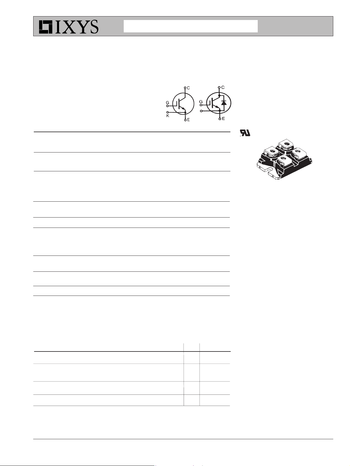
SOT-227B, miniBLOC
E153432
G = Gate, C = Collector, E = Emitter
either emitter terminal can be used as
Main or Kelvin Emitter
Features
International standard package
miniBLOC
UL recognized
Aluminium nitride isolation
- high power dissipation
Isolation voltage 3000 V~
Very high current IGBT
Low V
CE(sat)
conduction losses
MOS Gate turn-on
- drive simplicity
Low collector-to-case capacitance
(< 50 pF)
Low package inductance (< 5 nH)
E
G
E
C
for minimum on-state
- easy to drive and to protect
Applications
AC motor speed control
DC servo and robot drives
DC choppers
Uninterruptible power supplies (UPS)
Switch-mode and resonant-mode
power supplies
Advantages
Easy to mount with 2 screws
Space savings
High power density
© 2004 IXYS All rights reserved
DS99180(05/04)
Page 2
IXGN 80N60A2D1
Symbol Test Conditions Characteristic Values
= 25°C, unless otherwise specified)
(T
g
C
C
C
Q
Q
Q
t
t
t
t
E
t
t
E
t
t
E
fs
ies
oes
res
g
ge
gc
d(on)
ri
d(off)
fi
off
d(on)
ri
on
d(off)
fi
off
J
IC= 60 A; VCE = 10 V, Note 1 TBD S
VCE = 25 V, VGE = 0 V, f = 1 MHz TBD pF
IC = I
Inductive load, TJ = 25
IC = I
VCE = 0.8 V
Inductive load, TJ = 125
IC = I
VCE = 0.8 V
, VGE = 15 V, VCE = 0.5 V
C110
, VGE = 15 V
C110
C110
, RG = R
CES
, VGE = 15 V
, RG = R
CES
°°
°C
°°
= 2.0 Ω
off
°°
°C
°°
= 2.4 Ω
off
CES
min. typ. max.
TBD pF
TBD pF
TBD nC
TBD nC
TBD nC
TBD ns
TBD ns
TBD ns
250 ns
4mJ
TBD ns
TBD ns
TBD mJ
TBD ns
TBD ns
10 mJ
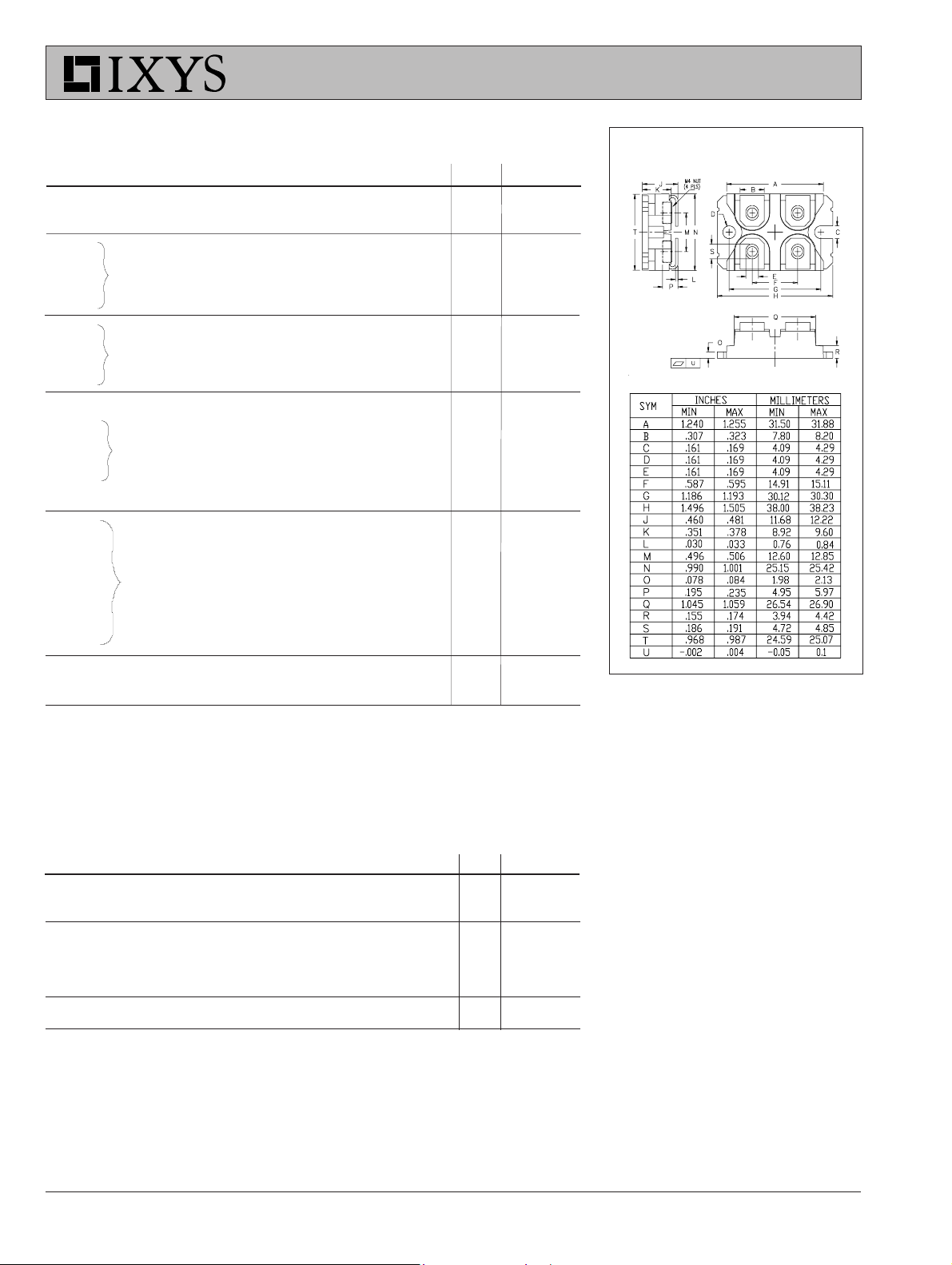
SOT-227B miniBLOC
R
thJC
R
thCK
0.05 K/W
0.2 K/W
Reverse Diode (FRED) Characteristic Values
= 25°C, unless otherwise specified)
(T
J
Symbol Test Conditions typ. max.
V
F
IF= 60 A, Note 1 2.05 V
TJ = 150°C 1.4 V
I
RM
IF= I
, VGE = 0 V, -diF/dt = 100 A/µs 8.0 A
C90
VR= 100 V, TJ = 100°C
t
rr
R
thJC
IF= 1 A, -di/dt = 50 A/µs, VR = 30 V 35 ns
1.65 K/W
Note: 1. Pulse test, t ≤ 300 µs, duty cycle d ≤ 2%
2. Remarks: Switching times may increase for
V
(Clamp) > 0.8 V
CE
3. Parts must be heatsunk for high temperature I
, higher TJ or increased R
CES
G
measurements
CES
IXYS reserves the right to change limits, test conditions, and dimensions.
IXYS MOSFETs and IGBTs are covered by one or more 4,850,072 4,931,844 5,034,796 5,063,307 5,237,481 5,381,025 6,404,065B1 6,162,665 6,534,343 6,583,505
of the following U.S. patents: 4,835,592 4,881,106 5,017,508 5,049,961 5,187,117 5,486,715 6,306,728B1 6,259,123B1 6,306,728B1 6,683,344
 Loading...