

Page 1
Low V
CE(sat)
IGBT with Diode
V
CES
I
C25
V
CE(sat)
High Speed IGBT with Diode
Combi Pack
IXGH 12N100U1 1000 V 24 A 3.5 V
IXGH 12N100AU1 1000 V 24 A 4.0 V
Symbol Test Conditions Maximum Ratings
V
CES
V
CGR
V
GES
V
GEM
I
C25
I
C90
I
CM
SSOA V
(RBSOA) Clamped inductive load, L = 300 mH @ 0.8 V
P
C
TJ= 25°C to 150°C 1000 V
TJ= 25°C to 150°C; RGE = 1 MW 1000 V
Continuous ±20 V
Transient ±30 V
TC= 25°C24A
TC= 90°C12A
TC= 25°C, 1 ms 48 A
= 15 V, TVJ = 125°C, RG = 150 W ICM = 24 A
GE
CES
TC= 25°C 100 W
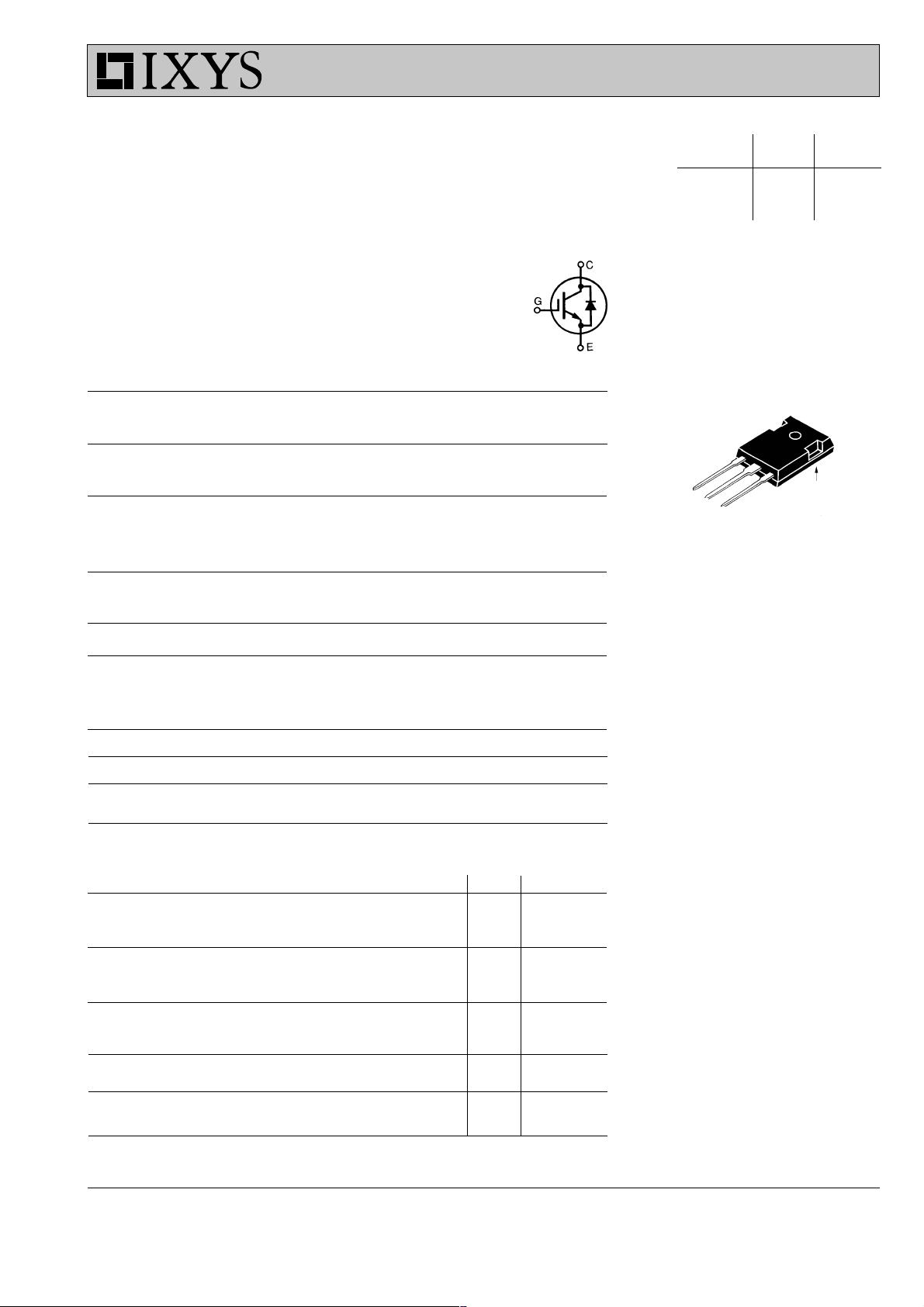
TO-247AD
G
C
E
G = Gate C = Collector
E = Emitter TAB = Collector
C (TAB)
T
J
T
JM
T
stg
M
d
Mounting torque with screw M3 1.13/1 0 Nm/lb.in.
Weight 6g
Maximum lead temperature for soldering 30 0 °C
1.6 mm (0.062 in.) from case for 10 s
-55 ... +150 °C
150 °C
-55 ... +150 °C
Features
• International standard packages
JEDEC TO-247
• IGBT with antiparallel FRED in one
package
• HDMOS
• Low V
- for minimum on-state conduction
• MOS Gate turn-on
Symbol Test Conditions Characteristic Values
(TJ = 25°C, unless otherwise specified) Min. Typ. Max.
BV
V
CES
GE(th)
IC= 3 mA, VGE = 0 V 1000 V
BV
temperature coefficient 0.072 %/K
CES
IC= 500 mA, VGE = V
V
temperature coefficient -0.192 %/K
GE(th)
GE
2.5 5.5 V
- drive simplicity
• Fast Recovery Expitaxial Diode (FRED)
- soft recovery with low I
Applications
• DC choppers
• AC motor speed control
• DC servo and robot drives
• Uninterruptible power supplies (UPS)
• Switch-mode and resonant-mode
I
CES
VCE = 0.8, V
CES
TJ = 25°C 300 mA
power supplies
VGE= 0 V TJ = 125°C5mA
Advantages
I
V
GES
CE(sat)
VCE= 0 V, VGE = ±20 V ±100 nA
IC= I
, VGE = 15 12N100U1 3.5 V
CE90
12N100AU1 4.0 V
• Easy to mount with one screw
• Reduces assembly time and cost
• Space savings (two devices in one
package)
CE(sat)
losses
TM
process
RM
IXYS reserves the right to change limits, test conditions, and dimensions.
© 2000 IXYS All rights reserved
95596C (7/00)
1 - 5
Page 2
IXGH12N100U1 IXGH12N100AU1
Symbol Test Conditions Characteristic Values
(TJ = 25°C, unless otherwise specified) Min. Typ. Max.
g
fs
IC= I
; VCE = 10 V, 6 10 S
C90
Pulse test, t £ 300 ms, duty cycle £ 2 %
C
C
C
Q
Q
Q
t
t
t
t
E
t
t
E
t
t
E
ies
oes
res
g
ge
gc
d(on)
ri
d(off)
fi
off
d(on)
ri
(on)
d(off)
fi
off
VCE= 25 V, VGE = 0 V, f = 1MHz 120 pF
IC= I
, VGE = 15 V, VCE = 0.5 V
C90
CES
Inductive load, TJ = 25°C
IC= I
VCE= 800 V, RG = R
Remarks: Switching times may
increase for V
higher T
, VGE = 15 V, L = 300 mH
C90
= 120 W
off
(Clamp) > 0.8 V
CE
or increased R
J
G
CES
12N100U1 800 1000 ns
12N100AU1 5 00 70 0 ns
,
12N100U1 2.5 mJ
12N100AU1 1.5 3.0 mJ
Inductive load, TJ = 125°C
IC= I
VCE= 800 V, RG = R
Remarks: Switching times may
increase for V
higher T
, VGE = 15 V, L = 300 mH
C90
= 120 W
off
(Clamp) > 0.8 V
CE
or increased R
J
G
CES
12N100U1 1250 ns
12N100AU1 9 50 ns
,
12N100U1 3.5 mJ
750 pF
30 pF
65 90 nC
820nC
24 45 nC
100 ns
200 ns
850 1000 ns
100 ns
200 ns
1.1 mJ
900 ns
12N100AU1 2.2 mJ
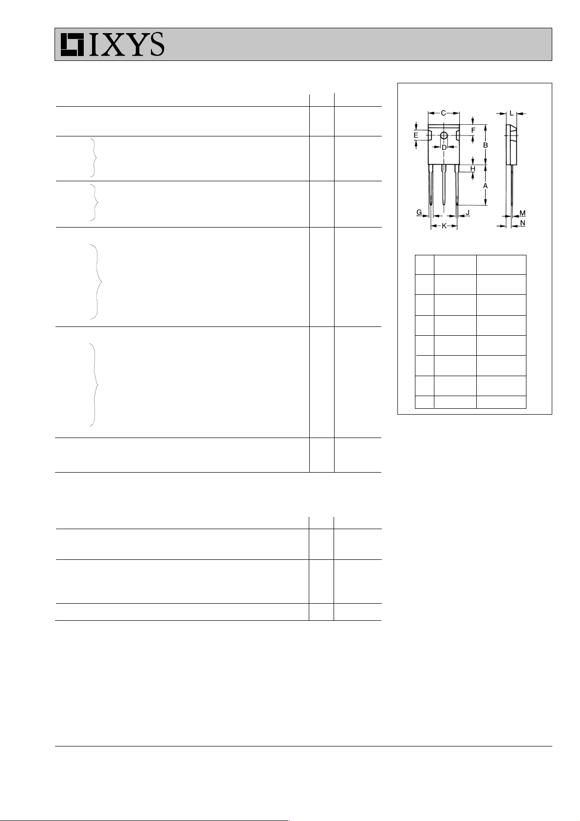
TO-247 AD (IXGH) Outline
Dim. Millimeter Inches
Min. Max. Min. Max.
A 19.81 20.32 0.780 0.800
B 20.80 21.46 0.819 0.845
C 15.75 16.26 0.610 0.640
D 3.55 3.65 0.140 0.144
E 4.32 5.49 0.170 0.216
F 5.4 6.2 0.212 0.244
G 1.65 2.13 0.065 0.084
H - 4.5 - 0.177
J 1.0 1.4 0.040 0.055
K 10.8 11.0 0.426 0.433
L 4.7 5.3 0.185 0.209
M 0.4 0.8 0.016 0.031
N 1.5 2.49 0.087 0.102
R
thJC
R
thCK
1.25 K/W
0.25 K/W
Reverse Diode (FRED) Characteristic Values
= 25°C, unless otherwise specified)
(T
J
Symbol Test Conditions Min. Typ. Max.
V
F
IF=8A, VGE = 0 V, 2.75 V
Pulse test, t £ 300 ms, duty cycle d £ 2 %
I
RM
t
rr
R
thJC
IF= I
, VGE = 0 V, -diF/dt = 100 A/ms 6.5 A
C90
VR= 540 V TJ = 125°C 120 ns
I
= 1 A, -di/dt = 50 A/ms, VR = 30 V TJ = 25°C5060ns
F
2.5 K/W
© 2000 IXYS All rights reserved
IXYS MOSFETS and IGBTs are covered by one or more of the following U.S. patents:
4,835,592 4,881,106 5,017,508 5,049,961 5,187,117 5,486,715
4,850,072 4,931,844 5,034,796 5,063,307 5,237,481 5,381,025
2 - 5
Page 3

IXGH12N100U1 IXGH12N100AU1
50
TJ = 25°C
40
VGE = 15V
13V
11V
9V
30
20
- Amperes
C
I
7V
10
0
0246810
VCE - Volts
Figure 1. Saturation Voltage Characteristics
50
TJ = 125°C
40
30
20
- Amperes
C
I
10
0
0246810
VGE = 15V
13V
11V
9V
VCE - Volts
Figure 3. Saturation Voltage Characteristics
7V
100
TJ = 25°C
VGE = 15V
80
60
40
- Amperes
C
I
20
0
048121620
VCE - Volts
Figure 2. Extended Output Characteristics
1.6
VGE = 15V
= 24A
I
C
1.4
1.2
I
= 12A
C
- Normalized
1.0
CE (sat)
V
0.8
IC = 6A
0.6
25 50 75 100 125 150
TJ - Degrees C
Figure 4. Temperature Dependence of V
13V
11V
9V
7V
CE(sat)
50
= 10V
V
CE
40
30
20
- Amperes
C
I
10
0
24681012
VGE - Volts
© 2000 IXYS All rights reserved
TJ = 25°C
T
= 125°C
J
Capacitance - pF
1000
C
iss
C
oss
f = 1Mhz
100
C
rss
10
0 5 10 15 20 25 30 35 40
VCE-Volts
Figure 6. Capacitance CurvesFigure 5. Admittance Curves
3 - 5
Page 4

IXGH12N100U1 IXGH12N100AU1
1200
TJ = 125°C
RG = 120
1100
t
1000
E
- nanoseconds
fi
t
900
(OFF)
800
0 5 10 15 20
IC - Amperes
Figure 7. Dependence of tfi and E
15
I
= 30A
C
= 150V
V
CE
12
9
- Volts
GE
6
V
5
E
(OFF)
4
1000
800
TJ = 125°C
I
t
fi
= 12A
C
- milliJoules
fi
600
5
4
E
(OFF)
- millijoules
3
3
400
E
- nanoseconds
2
1
fi
t
200
0
(OFF)
2
1
0
0306090120150
RG - Ohms
on IC.
OFF
Figure 8. Dependence of tfi and E
on RG.
OFF
100
24
10
- Amperes
C
1
I
TJ = 125°C
RG = 4.7
dV/dt < 5V/ns
3
0
0 1530456075
Qg - nanocoulombs
Figure 9. Gate Charge
1
D=0.5
D=0.2
D=0.1
0.1
D=0.05
0.01
D=0.02
D=0.01
Single pulse
(K/W)
thJC
Z
D = Duty Cycle
0.1
0 200 400 600 800 1000
VCE - Volts
Figure 10. Turn-off Safe Operating Area
0.001
0.00001 0.0001 0.001 0.01 0.1 1
Pulse Width - Seconds
© 2000 IXYS All rights reserved
Figure 11. Transient Thermal Resistance
4 - 5
Page 5

IXGH12N100U1 IXGH12N100AU1
Fig. 12. Forward current versus Fig. 13. Recovery charge versus -diF/dt. Fig. 14. Peak reverse current versus
voltage drop. -diF/dt.
Fig. 15. Dynamic parameters versus Fig. 16. Reverse recovery time . Fig. 17. Forward voltage recovery and
junction temperature. versus -diF/dt time versus -diF/dt.
Fig. 18. Transient thermal impedance junction to case.
© 2000 IXYS All rights reserved
5 - 5
 Loading...