

Page 1
HiPerFET
TM
Power MOSFETs
Q-Class
IXFH 15N80Q
IXFT 15N80Q
V
I
D25
R
DSS
DS(on)
= 800 V
= 15 A
= 0.60 W
N-Channel Enhancement Mode
Avalanche Rated, High dv/dt, Low Q
Symbol Test Conditions Maximum Ratings
V
DSS
V
DGR
V
GS
V
GSM
I
D25
I
DM
I
AR
E
AR
E
AS
dv/dt I
P
D
T
J
T
JM
T
stg
T
L
M
d
Weight TO-247 6 g
Symbol Test Conditions Characteristic Values
(TJ = 25°C, unless otherwise specified) Min. Typ. Max.
V
DSS
V
GS(th)
I
GSS
I
DSS
R
DS(on)
TJ= 25°C to 150°C 800 V
TJ= 25°C to 150°C; RGS = 1 MW 800 V
Continuous ±20 V
Transient ±30 V
TC= 25°C15A
TC= 25°C, pulse width limited by T
TC= 25°C15A
TC= 25°C30mJ
TC= 25°C 1.0 J
£ IDM, di/dt £ 100 A/ms, VDD £ V
S
£ 150°C, RG = 2 W
T
J
TC= 25°C 300 W
1.6 mm (0.062 in.) from case for 10 s 300 °C
Mounting torque 1.13/10 Nm/lb.in.
TO-268 4 g
VGS= 0 V, ID = 3 mA 800 V
VDS= VGS, ID = 4 mA 2.0 4.5 V
VGS= ±20 VDC, VDS = 0 ±100 nA
VDS= V
V
VGS= 10 V, ID = 0.5 I
DSS
= 0 V TJ = 125°C1mA
GS
D25
Pulse test, t £ 300 ms, duty cycle d £ 2 %
g
JM
, 5 V/ns
DSS
60 A
-55 ... +150 °C
150 °C
-55 ... +150 °C
TJ = 25°C25mA
0.60 W
trr £ 250 ns
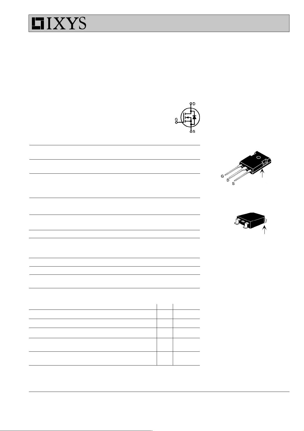
TO-247 AD (IXFH)
(TAB)
TO-268 (D3) (IXFT) Case Style
G
S
G = Gate D = Drain
S = Source TAB = Drain
Features
• IXYS advanced low Qg process
• International standard packages
• Low R
• Unclamped Inductive Switching (UIS)
DS (on)
rated
• Fast switching
• Molding epoxies meet UL 94 V-0
flammability classification
Advantages
• Easy to mount
• Space savings
• High power density
(TAB)
IXYS reserves the right to change limits, test conditions, and dimensions.
© 2000 IXYS All rights reserved
98514B (7/00)
1 - 4
Page 2
IXFH 15N80Q
IXFT 15N80Q
Symbol Test Conditions Characteristic Values
(TJ = 25°C, unless otherwise specified)
Min. Typ. Max.
g
C
C
C
t
t
t
t
Q
Q
Q
R
R
fs
iss
oss
rss
d(on)
r
d(off)
f
g(on)
gs
gd
thJC
thCK
VDS= 10 V; ID = 0.5 I
, pulse test 8 16 S
D25
4300 pF
VGS = 0 V, VDS = 25 V, f = 1 MHz 36 0 pF
60 pF
18 ns
VGS = 10 V, VDS = 0.5 V
, ID = 0.5 I
DSS
D25
27 ns
RG = 1.5 W (External) 53 ns
16 ns
90 nC
VGS = 10 V, VDS = 0.5 V
, ID = 0.5 I
DSS
D25
20 nC
30 nC
0.42 K/W
(TO-247) 0.25 K/W
Source-Drain Diode Characteristic Values
(TJ = 25°C, unless otherwise specified)
Symbol Test Conditions min. typ. max.
I
S
I
SM
V
SD
VGS = 0 V 15 A
Repetitive; 60 A
IF = IS, VGS = 0 V, 1.5 V
Pulse test, t £ 300 ms, duty cycle d £ 2 %
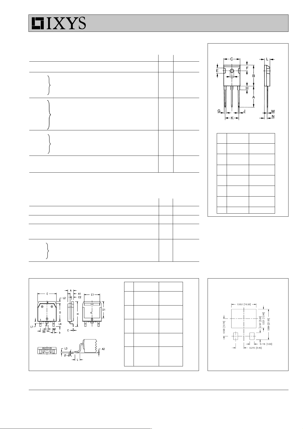
TO-247 AD (IXFH) Outline
Dim. Millimeter Inches
Min. Max. Min. Max.
A 19.81 20.32 0.780 0.800
B 20.80 21.46 0.819 0.845
C 15.75 16.26 0.610 0.640
D 3.55 3.65 0.140 0.144
E 4.32 5.49 0.170 0.216
F 5.4 6.2 0.212 0.244
G 1.65 2.13 0.065 0.084
H - 4.5 - 0.177
J 1.0 1.4 0.040 0.055
K 10.8 11.0 0.426 0.433
L 4.7 5.3 0.185 0.209
M 0.4 0.8 0.016 0.031
N 1.5 2.49 0.087 0.102
t
rr
Q
RM
I
RM
IF = IS-di/dt = 100 A/ms, VR = 100 V 0.85 mC
TO-268AA (D3 PAK)
8A
Dim. Millimeter Inches
Min. Max. Min. Max.
A 4.9 5.1 .193 .201
A
2.7 2.9 .106 .114
1
A2.02 .25 .001 .010
b 1.15 1.45 .045 .057
b
1.9 2.1 .75 .83
2
C .4 .65 .016 .026
D 13.80 14.00 .543 .551
E 15.85 16.05 .624 .632
13.3 13.6 .524 .535
E
1
e 5.45 BSC .215 BSC
H 18.70 19.10 .736 .752
L 2.40 2.70 .094 .106
L1 1.20 1.40 .047 .055
L2 1.00 1.15 .039 .045
L3 0.25 BSC .010 BSC
L4 3.80 4.10 .150 .161
250 ns
Min. Recommended Footprint
© 2000 IXYS All rights reserved
IXYS MOSFETS and IGBTs are covered by one or more of the following U.S. patents:
4,835,592 4,881,106 5,017,508 5,049,961 5,187,117 5,486,715
4,850,072 4,931,844 5,034,796 5,063,307 5,237,481 5,381,025
2 - 4
Page 3

IXFH 15N80Q
IXFT 15N80Q
20
TJ = 25OC
16
= 9V
V
GS
8V
7V
6V
12
8
- Amperes
D
I
4
0
0246810
VDS - Volts
2.6
V
= 10V
2.4
2.2
GS
= 125OC
T
J
2.0
1.8
1.6
- Normalized
1.4
DS(ON)
1.2
R
TJ = 25OC
1.0
0.8
0 5 10 15 20 25
ID - Amperes
5V
4V
20
= 125OC
T
J
16
V
= 9V
GS
8V
7V
6V
12
8
- Amperes
D
I
4
0
0 4 8 12 16 20
VDS - Volts
Figure 2. Output Characteristics at 125OCFigure 1. Output Characteristics at 25OC
2.6
V
= 10V
2.4
2.2
2.0
1.8
- Normalized
1.6
DS(ON)
1.4
R
1.2
1.0
25 50 75 100 125 150
GS
TJ - Degrees C
I
= 15A
D
ID = 7.5A
5V
4V
Figure 3. R
20
normalized to value at ID = 12A
DS(on)
Figure 4. R
16
14
normalized to value at ID = 12A
DS(on)
16
12
10
12
IXFH15N80
IXFH14N80
8
8
- Amperes
D
I
4
- Amperes
6
D
I
4
T
= 125oC
J
TJ = 25oC
2
0
-50 -25 0 25 50 75 100 125 150
TC - Degrees C
0
234567
VGS - Volts
Figure 5. Drain Current vs. Case Temperature Figure 6. Admittance Curves
© 2000 IXYS All rights reserved
3 - 4
Page 4

IXFH 15N80Q
IXFT 15N80Q
12
10
8
6
- Volts
GS
V
4
V
I
I
= 400 V
DS
= 7.5 A
D
= 10 mA
G
2
0
0 20406080100120
Gate Charge - nC
Figure 7. Gate Charge
50
40
30
TJ = 125OC
20
- Amperes
D
I
TJ = 25OC
10
0
0.2 0.4 0.6 0.8 1.0 1.2 1.4 1.6
VSD - Volts
Figure 9. Source Current vs. Source to Drain Voltage
1.00
- Amperes
I
Capacitance - pF
D
10000
1000
100
Ciss
Crss
f = 1MHz
Coss
10
0 5 10 15 20 25 30 35
VDS - Volts
Figure 8. Capacitance Curves
100
60
10
1
TC = 25OC
0. 1
10 100 1000
V
- Volts
DS
Figure10. Forward Bias Safe Operating
Area
0.1 ms
1 ms
10
ms
100
ms
DC
D=0.5
0.10
D=0.2
0.01
0.00
D=0.1
D=0.05
D=0.02
D=0.01
Single Pulse
-5
10
10
- K/W
R(th)
JC
Figure 11. Transient Thermal Resistance
© 2000 IXYS All rights reserved
-4
10
-3
10
-2
10
-1
10
0
10
1
Pulse Width - Seconds
4 - 4
 Loading...