

Page 1
HiPerFET
ISOPLUS247
TM
Power MOSFETs
TM
(Electrically Isolated Back Surface)
N-Channel Enhancement Mode
High dV/dt, Low trr, HDMOSTM Family
Preliminary data
V
DSS
I
D25
R
DS(on)
IXFR 30N50Q 500 V 29 A 0.16 W
IXFR 32N50Q 500 V 30 A 0.15 W
t
£ 250 ns
rr
Symbol Test Conditions Maximum Ratings
V
DSS
V
DGR
V
GS
V
GSM
I
D25
I
DM
I
AR
E
AS
E
AR
dv/dt IS£ IDM, di/dt £ 100 A/ms, VDD £ V
P
D
T
J
T
JM
T
stg
T
L
V
ISOL
TJ= 25°C to 150°C 500 V
TJ= 25°C to 150°C; RGS = 1 MW 500 V
Continuous ±20 V
Transient ±30 V
TC= 25°C 30N50 30 A
32N50
TC= 25°C, Pulse width limited by T
30N50 120 A
JM
32N50
TC= 25°C 30N50 30 A
32N50
TC= 25°C 1.5 J
TC= 25°C45mJ
5 V/ns
TJ£ 150°C, RG = 2 W
DSS
TC= 25°C 310 W
-55 ... +150 °C
150 °C
-55 ... +150 °C
1.6 mm (0.062 in.) from case for 10 s 300 °C
50/60 Hz, RMS t = 1 minute leads-to-tab 2500 V~
Weight 6 g
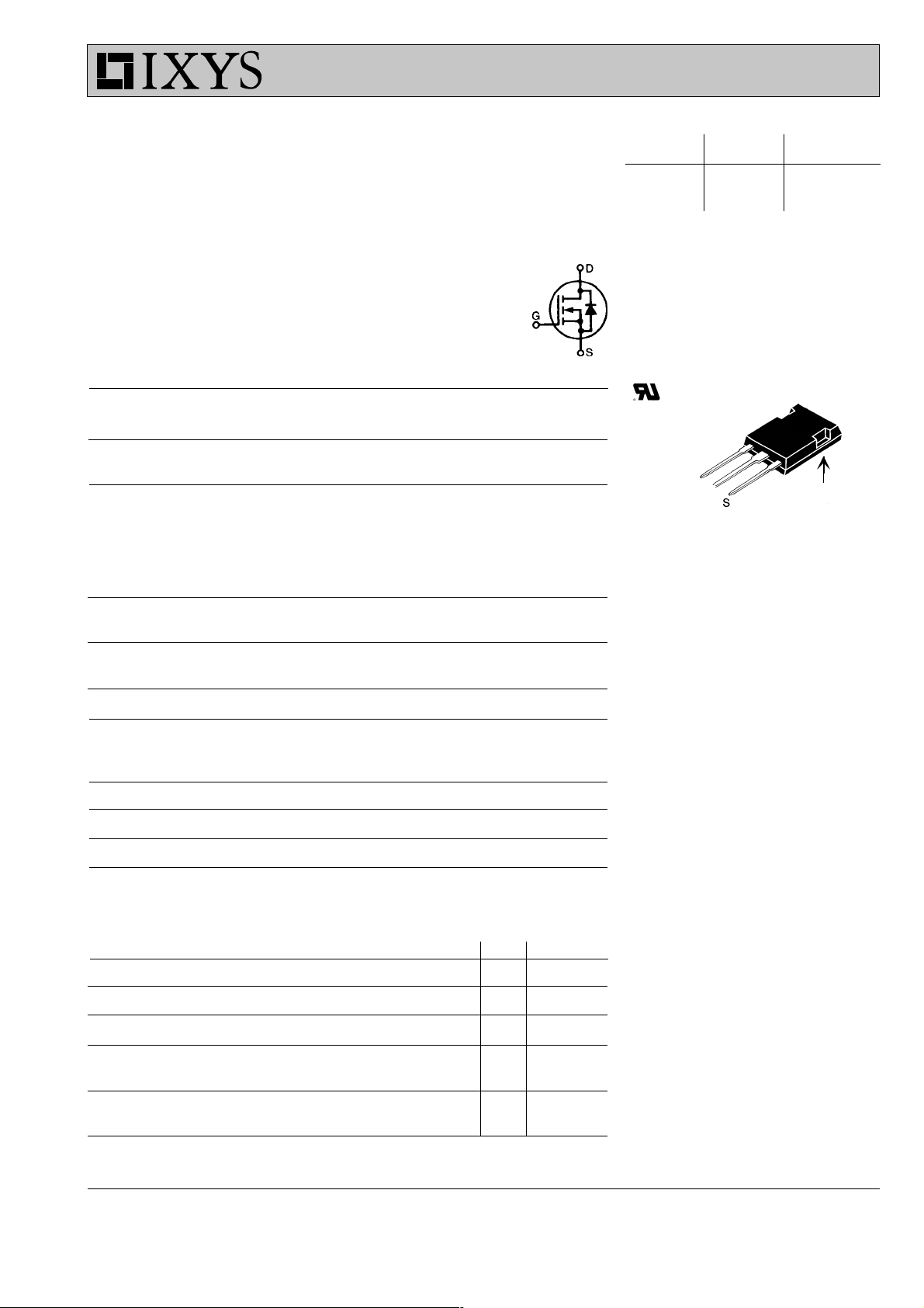
ISOPLUS 247
G = Gate D = Drain
S = Source
* Patent pending
Features
• Silicon chip on Direct-Copper-Bond
• Low drain to tab capacitance(<50pF)
• Low R
• Rugged polysilicon gate cell structure
• Unclamped Inductive Switching (UIS)
• Fast intrinsic Rectifier
TM
E 153432
G
D
Isolated back surface*
substrate
- High power dissipation
- Isolated mounting surface
- 2500V electrical isolation
HDMOSTM process
DS (on)
rated
Symbol Test Conditions Characteristic Values
(TJ = 25°C, unless otherwise specified)
min. typ. max.
V
V
I
I
R
GSS
DSS
DSS
GS(th)
DS(on)
V
V
= 0 V, ID = 1mA 500 V
GS
= VGS, ID = 4mA 2 4 V
DS
VGS = ±20 VDC, VDS = 0 ±100 nA
VDS = V
V
DSS
= 0 V TJ = 125°C 1mA
GS
VGS = 10 V, ID = I
T
TJ = 25°C 100 mA
30N50 0.16 W
Notes 1, 2 32N50 0.15 W
IXYS reserves the right to change limits, test conditions, and dimensions.
© 2000 IXYS All rights reserved
Applications
DC-DC converters
• Battery chargers
• Switched-mode and resonant-mode
power supplies
• DC choppers
• AC motor control
Advantages
• Easy assembly
• Space savings
• High power density
98608B (7/00)
1 - 4
Page 2
IXFR 30N50Q
IXFR 32N50Q
Symbol Test Conditions Characteristic Values
(TJ = 25°C, unless otherwise specified)
min. typ. max.
g
C
C
C
t
t
t
t
Q
Q
Q
R
R
fs
iss
oss
rss
d(on)
r
d(off)
f
g(on)
gs
gd
thJC
thCK
VDS= 10 V; ID = I
T
Note 2 18 28 S
3950 pF
VGS = 0 V, VDS = 25 V, f = 1 MHz 640 pF
210 pF
35 ns
VGS = 10 V, VDS = 0.5 • V
DSS
, ID = I
T
42 ns
RG = 1 W (External), 75 ns
20 ns
150 nC
VGS = 10 V, VDS = 0.5 • V
DSS
, ID = I
T
26 nC
85 nC
0.15 K/W
0.40 K/W
Source-Drain Diode Characteristic Values
(TJ = 25°C, unless otherwise specified)
Symbol Test Conditions min. typ. max.
I
S
I
SM
VGS= 0 V 32 A
Repetitive; pulse width limited by T
JM
128 A
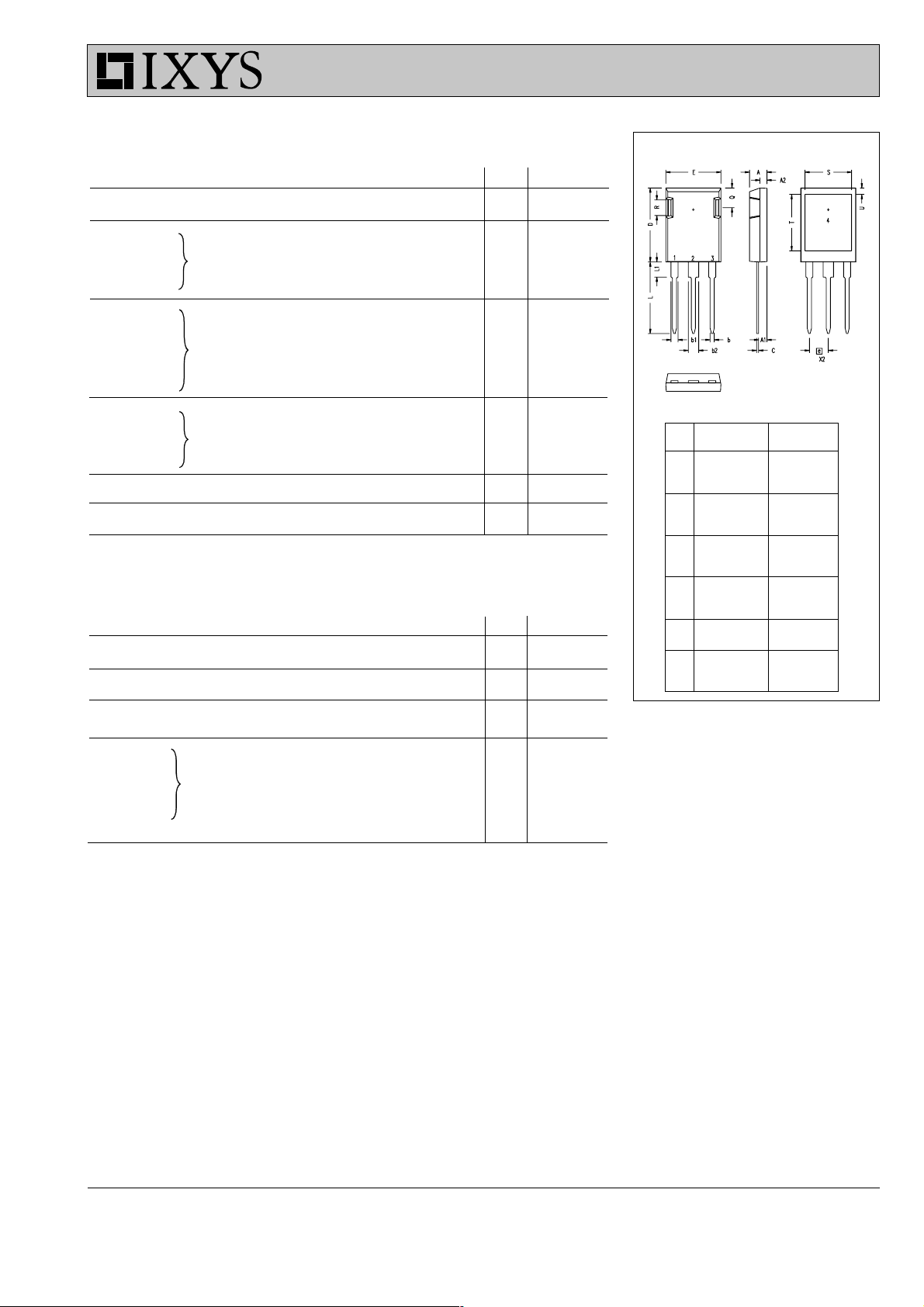
ISOPLUS 247 (IXFR) OUTLINE
1 Gate, 2 Drain (Collector)
3 Source (Emitter)
4 no connection
Dim. Millimeter Inches
Min. Max. Min. Max.
A 4.83 5.21 .190 .205
A
2.29 2.54 .090 .100
1
A21.91 2.16 .075 .085
b 1.14 1.40 .045 .055
1.91 2.13 .075 .084
b
1
b22.92 3.12 .115 .123
C 0.61 0.80 .024 .031
D 20.80 21.34 .819 .840
E 15.75 16.13 .620 .635
e 5.45 BSC .215 BSC
L 19.81 20.32 .780 .800
L1 3.81 4.32 .150 .170
Q 5.59 6.20 .220 .244
R 4.32 4.83 .170 .190
S 13.21 13.72 .520 .540
T 15.75 16.26 .620 .640
U 1.65 3.03 .065 .080
V
SD
t
rr
Q
RM
I
RM
IF = IS, VGS = 0 V, Note 1 1.5 V
IF = Is,
-di/dt = 100 A/ms,
VR = 100 V
Note: 1. IT test condition:
IXFR30N50: I
IXFR32N50: I
= 15A
T
= 16A
T
Note: 2. Pulse test, t £ 300 ms,
duty cycle d £ 2 %
250 ns
0.75 mC
7.5 A
© 2000 IXYS All rights reserved
IXYS MOSFETS and IGBTs are covered by one or more of the following U.S. patents:
4,835,592 4,881,106 5,017,508 5,049,961 5,187,117 5,486,715
4,850,072 4,931,844 5,034,796 5,063,307 5,237,481 5,381,025
2 - 4
Page 3

IXFR 30N50Q
IXFR 32N50Q
Figure 1. Output Characteristics at 25OC Figure 2. Output Characteristics at 125OC
80
70
60
TJ = 25OC
VGS=10V
9V
8V
7V
50
40
- Amperes
30
D
I
20
10
0
0 4 8 12 16 20
VDS - Volts
Figure 3. R
normalized to 15A/25OC vs. I
DS(on)
2.8
V
= 10V
GS
2.4
Tj=125
0
C
2.0
- Normalized
1.6
DS(ON)
R
1.2
Tj=25
50
= 125OC
6V
40
T
J
VGS= 9V
8V
7V
6V
30
5V
20
- Amperes
D
I
5V
10
4V
0
0 4 8 121620
VDS - Volts
D
Figure 4. R
normalized to 15A/25OC vs. T
DS(on)
J
2.8
V
= 10V
GS
2.4
ID = 32A
2.0
- Normalized
1.6
0
C
DS(ON)
R
1.2
ID = 16A
0.8
0 102030405060
ID - Amperes
Figure 5. Drain Current vs. Case Temperature
40
32
24
16
- Amperes
D
I
8
0
-50-250 255075100125150
TC - Degrees C
0.8
25 50 75 100 125 150
TJ - Degrees C
Figure 6. Admittance Curves
50
40
30
20
- Amperes
D
I
T
= 125oC
J
T
= 25oC
J
10
0
23456
VGS - Volts
© 2000 IXYS All rights reserved
3 - 4
Page 4

I
-
Amperes
V
V
l
IXFR 30N50Q
IXFR 32N50Q
Figure 7. Gate Charge Figure 8. Capacitance Curves
14
Vds=300V
Vds=300V
=30A
=16A
I
I
D
D
=10mA
=10mA
I
I
G
G
ts
o
-
GS
12
10
8
6
4
2
0
0 50 100 150 200 250
Gate Charge - nC
Figure 9. Forward Voltage Drop of the
Intrinsic Diode
100
V
= 0V
GS
80
60
Capacitance - pF
10000
Ciss
Coss
1000
Crss
100
0 5 10 15 20 25
VDS - Volts
F = 1MHz
F = 1MHz
40
D
TJ=125OC
20
=25OC
=25OC
T
T
J
J
0
0.4 0.6 0.8 1.0 1.2
VSD - Volts
Figure 10. Transient Thermal Resistance
0.60
0.40
0.20
0.10
- K/W
0.08
JC
0.06
0.04
R(th)
0.02
0.01
-3
10
10
-2
10
-1
10
0
10
1
Pulse Width - Seconds
© 2000 IXYS All rights reserved
4 - 4
 Loading...