

Page 1
Preliminary Technical Information
PolarHVTMHiPerFET
Power MOSFET
(Electrically Isolated Tab)
IXFP 8N50PM
V
I
D25
R
trr
N-Channel Enhancement Mode
Avalanche Rated
Fast Intrinsic Diode
Symbol Test Conditions Maximum Ratings
V
DSS
V
DGR
V
GS
V
GSM
I
D25
I
DM
I
AR
E
AR
E
AS
dv/dt I
P
D
T
J
T
JM
T
stg
T
L
T
SOLD
M
d
Weight 4g
Symbol Test Conditions Characteristic Values
(TJ = 25° C unless otherwise specified) Min. Typ. Max.
BV
DSS
V
GS(th)
I
GSS
I
DSS
TJ= 25° C to 150° C 500 V
TJ= 25° C to 150° C; RGS = 1 MΩ 500 V
Continuous ±30 V
Transient ±40 V
TC= 25° C 4.4 A
TC= 25° C, pulse width limited by T
TC= 25° C8A
TC= 25° C20mJ
TC= 25° C 300 mJ
≤ IDM, di/dt ≤ 100 A/µs, VDD ≤ V
S
TJ≤ 150° C, RG = 18 Ω
TC= 25° C42W
1.6 mm (0.062 in.) from case for 10 s 300 °C
Plastic body for 10 s 260 °C
Mounting torque 1.13/10 Nm/lb.in.
VGS= 0 V, ID = 250 µA 500 V
VDS= VGS, ID = 1 mA 3.0 5.5 V
VGS= ±30 VDC, VDS = 0 ±100 nA
VDS= V
VGS= 0 V TJ = 125° C 500 µA
DSS
JM
, 10 V/ns
DSS
-55 ... +150 °C
-55 ... +150 °C
14 A
150 °C
5 µA
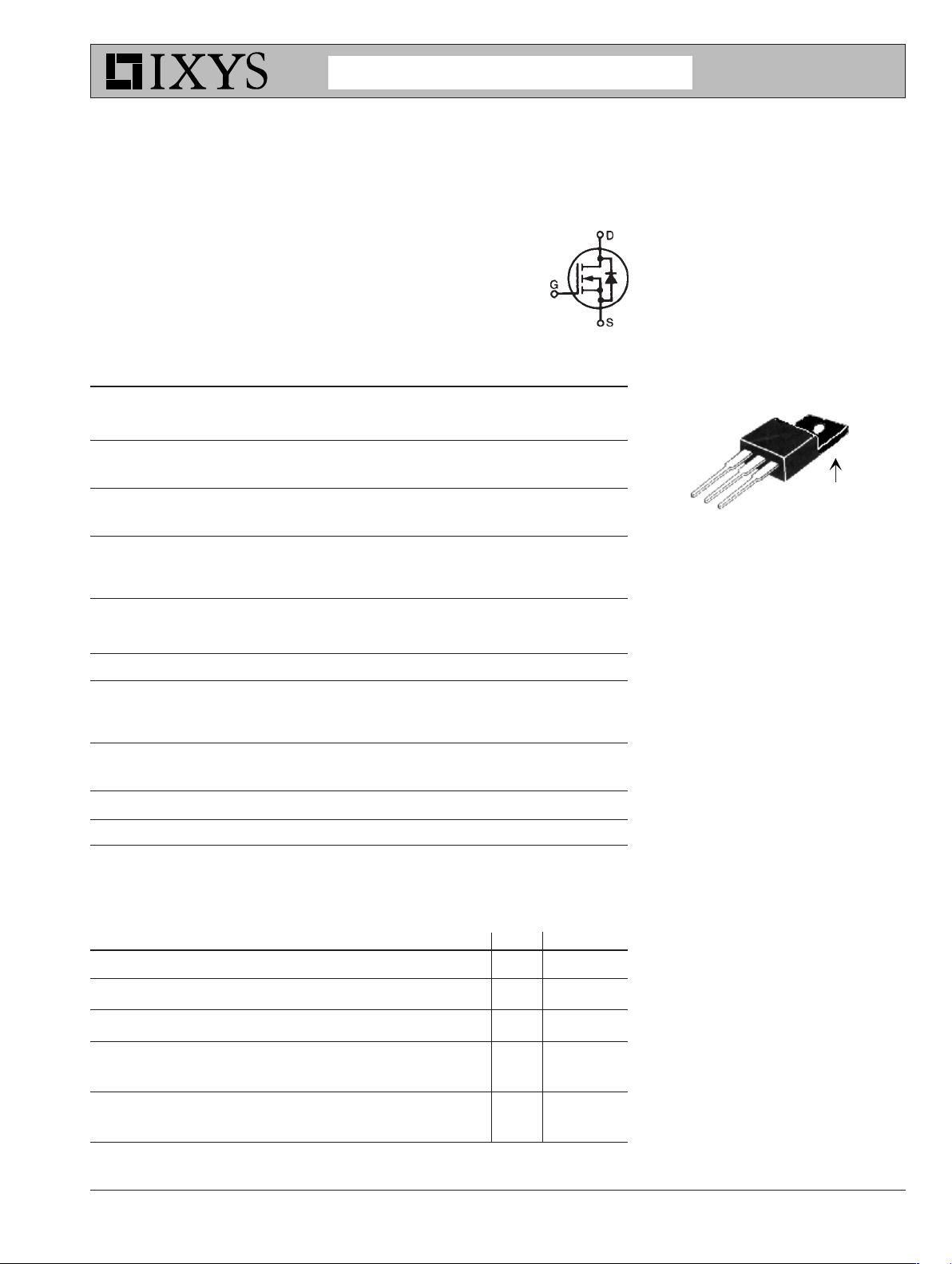
OVERMOLDED TO-220
(IXTP...M) OUTLINE
Features
l
Plastic overmolded tab for electrical
isolation
l
International standard package
l
Unclamped Inductive Switching (UIS)
rated
l
Low package inductance
- easy to drive and to protect
l
Fast Intrinsic Diode
Advantages
l
Easy to mount
l
Space savings
l
High power density
DSS
= 500 V
= 4.4 A
≤≤
≤ 0.8
DS(on)
G
≤≤
≤≤
≤ 200 ns
≤≤
Isolated Tab
D
S
G = Gate D = Drain
S = Source
ΩΩ
Ω
ΩΩ
R
DS(on)
© 2006 IXYS All rights reserved
VGS= 10 V, ID = 4 A 0.8 Ω
Pulse test, t ≤ 300 µs, duty cycle d ≤ 2 %
DS99484E(04/06)
Page 2
IXFP 8N50PM
Symbol Test Conditions Characteristic Values
= 25° C unless otherwise specified)
J
Min. Typ. Max.
1050 pF
12 pF
22 ns
23 ns
20 nC
7nC
3.0 ° C/W
g
C
C
C
t
t
t
t
Q
Q
Q
R
fs
iss
oss
rss
d(on)
r
d(off)
f
g(on)
gs
gd
thJS
(T
VDS= 10 V; ID = 4 A 5 8 S
VGS = 0 V, VDS = 25 V, f = 1 MHz 120 pF
VGS = 10 V, VDS = 0.5 V
, ID = 8 A 28 ns
DSS
RG = 18 Ω (External) 65 ns
VGS= 10 V, VDS = 0.5 V
, ID = 4 A 7 nC
DSS
Source-Drain Diode Characteristic Values
(TJ = 25° C, unless otherwise specified)
Symbol Test Conditions Min. Typ. Max.
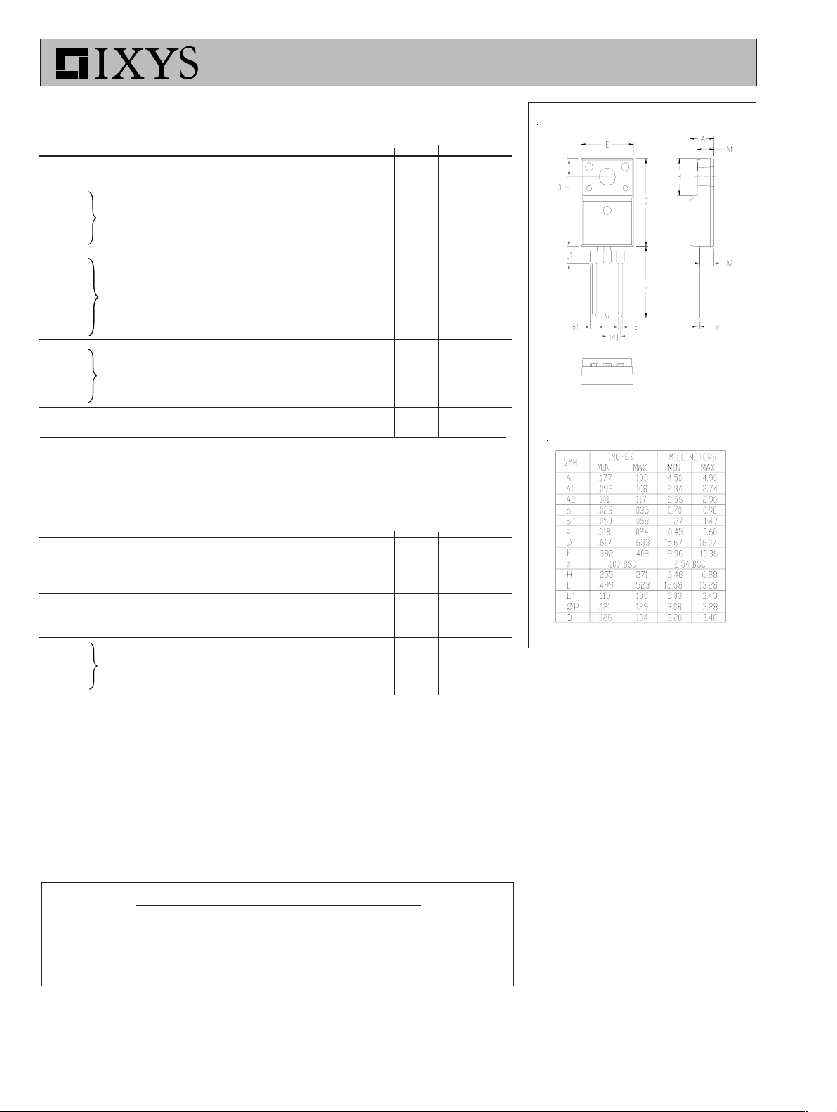
ISOLATED TO-220 (IXTP...M)
123
Terminals: 1 - Gate
2 - Drain (Collector)
3 - Source (Emitter)
I
S
I
SM
V
SD
VGS = 0 V 8 A
Repetitive 14 A
IF = IS, VGS = 0 V, 1.5 V
Pulse test, t ≤ 300 µs, duty cycle d ≤ 2 %
t
rr
Q
RM
I
RM
IF = 8 A, VGS=0V, VR=100V 200 ns
-di/dt = 100 A/µs 0.25 µC
2A
PRELIMINARY TECHNICAL INFORMATION
The product presented herein is under development. The Technical Specifications offered
are derived from data gathered during objective characterizations of preliminary engineering lots; but also may yet contain some information supplied during a pre-production
design evaluation. IXYS reserves the right to change limits, test conditions, and dimensions without notice.
IXYS reserves the right to change limits, test conditions, and dimensions.
IXYS MOSFETs and IGBTs are covered by 4,835,592 4,931,844 5,049,961 5,237,481 6,162,665 6,404,065 B1 6,683,344 6,727,585
one or moreof the following U.S. patents: 4,850,072 5,017,508 5,063,307 5,381,025 6,259,123 B1 6,534,343 6,710,405B2 6,759,692
4,881,106 5,034,796 5,187,117 5,486,715 6,306,728 B1 6,583,505 6,710,463 6,771,478 B2
 Loading...